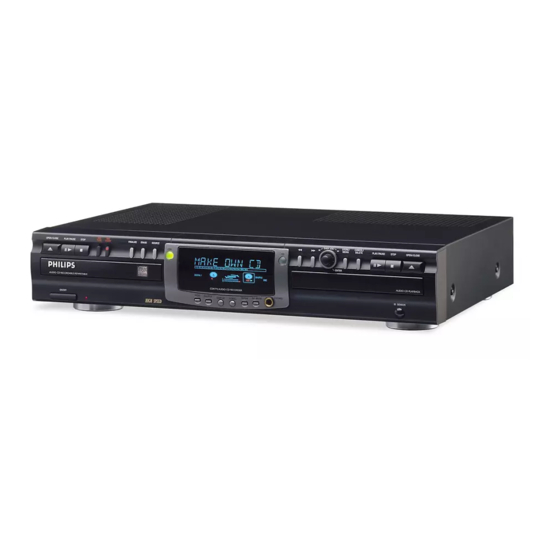
Philips CDR775 Service Manual
Hide thumbs
Also See for CDR775:
- Service manual (50 pages) ,
- Instructions for use manual (35 pages) ,
- Owner's manual (31 pages)
Table of Contents
Advertisement
Compact disc recorder
SERVICING
For servicing CDR775, the set can divided into three parts.
1. The display board (partly) 1 002, the I/O board 1004, the
headphone board (partly) 1002, the IR board (partly) 1002, the ON/
OFF & Standby LED board (partly) 1002 and the CD-out board
(partly) 1002 have to be repaired at component level. The power
supply unit 1003 is available as spare part, but can also be repaired
at component level.
2. The CDR module (containing the CDR loader 81, CDR main board
1001 and loader bracket 82, 83) will be exchanged completely in
case of failure. This complete CDR module is available as spare
part. Defective modules have to be returned for central repair.
3. The CD module (containing the CD loader 131, CD main board
1005 and loader bracket 132) is a new module with VAL1250
loader assy but also a separate CDM and separate loader parts will
be available via service stock. The CD main board can be repaired
at component level.
Also available: Circuit Description " The Basics of Compact Disc
Recordable/Rewriteable". Service code number 4822 725 25242.
©
Copyright reserved 1999 Philips Consumer Electronics B.V. Eindhoven, The
Netherlands. All rights reserved. No part of this publication may be reproduced,
stored in a retrieval system or transmitted, in any form or by any means, electronic,
mechanical, photocopying, or otherwise without the prior permission of Philips.
Published by RH 9969 Service DPS Hasselt
OPEN / CLOSE
OPEN / CLOSE
OPEN / CLOSE
PLAY / PAUSE
PLAY / PAUSE
PLAY / PAUSE
AUDIO CD RECORDAB LE/REWRITA
AUDIO CD RECORDAB LE/REWRITA
AUDIO CD RECORDAB LE/REWRITA
ON / OFF
Printed in the Netherlands
REC
STOP
STOP
STOP
TYPE
RECORD
EXT
EXT
FINALIZE
FINALIZE
ERASE
ERASE
SOURCE
SOURCE
Recordable
BLE
BLE
BLE
CDR775 AUDIO CD RECORDER
PROG
SHUFFLE
PHONES
SCROLL
REPEAT
DJ MODE
Contents
1. Technical Specifications
2. Warning and Servicing Hints
Wiring Diagram CDR
Wiring Diagram CD loader
Exploded View CDR
Exploded View CD loader
Dismantling Instructions
Overall Blockdiagram
IR / On/Off &Standby LED Board
Headphone / CD-out Board
I/O Board
Cd-Mainboard 1A
CD-Mainboard 1B
CD-Mainboard 1C
CD-Mainboard 2
10. Partslist (mechanical and electrical)
Subject to modification
CDR775
/00
5
5
6
6
J
EASY JOG
EASY JOG
STORE/
J
K
K
STORE/
CANCEL/
CANCEL/
MENU
MENU
DELETE
DELETE
PLAY/PAUSE
PLAY/PAUSE
STOP
STOP
OPEN/CLOSE
OPEN/CLOSE
ENTER
AUDIO CD PLAYBACK
AUDIO CD PLAYBACK
IR SENSOR
CL 96532086_000.eps
080999
Page
2
4
7
19
19
20
21
22
23
Diagram PWB
24
26
26
27
27
28
28
29
30
31
32
33
37/38
34
37/38
35
37/38
36
37/38
39
43
49
65
71
5 3104 125 40030
Advertisement
Table of Contents
Troubleshooting

Related Manuals for Philips CDR775


Summary of Contents for Philips CDR775
- Page 1 Contents Page 1. Technical Specifications 2. Warning and Servicing Hints For servicing CDR775, the set can divided into three parts. 3. User Instructions 4. Mechanical Instructions 1. The display board (partly) 1 002, the I/O board 1004, the Wiring Diagram CDR...
-
Page 2: Technical Specifications
GB 2 CDR775 Technical Specifications CDR775 1. Technical Specifications CDR775 General and 20kHz (typical >93dB) S/N-ratio A-weighted : > 98dB (typical Mains voltage : all range version 84- 100dB) 230V (/00, /01C, /06, / S/N-ratio unweighted : > 95dB (typical 98dB) - Page 3 Technical Specifications CDR775 CDR775 GB 3 1.3.4 Headphone output (all functions) Output voltage : 3Vrms (0dB)/8-2000Ω : > 80dB THD+N : > 78dB Channel separation : > 60dB between 20Hz and 20kHz Laser device Material : GaAlAs Wave length : between 780 and 800nm (at 25°C)
-
Page 4: Warning And Servicing Hints
GB 4 CDR775 Warnings and Servicing Hints 2. Warnings and Servicing Hints WARNING WAARSCHUWING All ICs and many other semi-conductors are Alle IC's en vele andere halfgeleiders zijn susceptible to electrostatic discharges (ESD). gevoelig voor elektrostatische ontladingen Careless handling during repair can reduce (ESD). - Page 5 Warnings and Servicing Hints CDR775 GB 5 SERVICING HINTS In the set, chip components have been applied. For disassembly and assembly check the figure below. CL 96532086_022.eps 080999...
- Page 6 GB 6 CDR775 Warnings and Servicing Hints CL 96532086_023.eps 080999...
-
Page 7: User Instructions
User instructions CDR775 GB 7 3. User instructions... - Page 8 GB 8 CDR775 User instructions...
- Page 9 User instructions CDR775 GB 9...
- Page 10 GB 10 CDR775 User instructions...
- Page 11 User instructions CDR775 GB 11...
- Page 12 GB 12 CDR775 User instructions...
- Page 13 User instructions CDR775 GB 13...
- Page 14 GB 14 CDR775 User instructions...
- Page 15 User instructions CDR775 GB 15...
- Page 16 GB 16 CDR775 User instructions...
- Page 17 User instructions CDR775 GB 17...
- Page 18 GB 18 CDR775 User instructions Personal notes:...
-
Page 19: Mechanical Instructions
Mechanical instructions CDR775 GB 19 4. Mechanical instructions Wiring diagram WIRING DIAGRAM CDR775 Pin 1 indicated by All Wires are 1/1, except flex 8001, 8005 and 8007 0101 8006 8001 (at conn. 1400 8002 8003 (at conn. F934 3104 157 1099... -
Page 20: Wiring Diagram Cd Loader
Mechanical instructions CDR775 GB 20 Wiring CD WIRING DIAGRAM CD LOADER VAL1250 CONNECTOR 1006 CONNECTOR 1002 Connection tray motor and tray switch HALL + HOMESW SGND TRAY+ TRAY- HALL- LOADER VAL1250 CONNECTOR 1001 Tray HOMESW 1002 switch UCOIL SGND 1208... -
Page 21: Exploded View Cdr
Mechanical instructions CDR775 GB 21 Exploded view CDR775 EXPLODED VIEW CDR775 LOADER ASSY CD LOADER ASSY CDR MAIN BOARD CDR CD OUT BOARD MAIN BOARD I/O BOARD ON/OFF POWER SUPPLY UNIT & STBY LED DISPLAY BOARD HEADPHONE BOARD BOARD CL 96532086_003.eps... -
Page 22: Exploded View Cd Loader
Mechanical instructions CDR775 GB 22 Exploded view CD EXPLODED VIEW CD LOADER VAL1250 CLAMPER ASSY SUSPENSION CDM VAM1250 RACK SPRING MOTORSPRING SCREW SCREW SUSPENSION RACK SUB CHASSIS RUBBER RUBBER SWITCH SUSPENSION RUBBER PLUG SUSPENSION TRAY GEARWHEEL RUBBER PLUG TULE CHASSIS ASSY VAL1250... -
Page 23: Dismantling Instructions
Mechanical instructions CDR775 GB 23 Dismantling 775 DISMANTLING INSTRUCTIONS CDR775 See exploded views for item numbers Cover 165 assembling ↑ ⇒ → 172, Remove 7 screws 166 ↓ 2 at each side and 3 at rear side. ⇒ disassembling Lift cover at rear side to remove. - Page 24 Electrical and circuit diagrams CDR775 GB 24 5. Electrical and circuit diagrams Blockdiagram 775 OVERALL BLOCK DIAGRAM CDR775 CDR MAIN BOARD ON/OFF CDL 4009 1302 LOADER ASSY 2 WIRES 7703 7330 1500 CDM3800 0205 0206 1330 FLASH HALL +12V 11 WIRES...
- Page 25 CDR775 GB 25 Display 775 0100 G10 F146 E7 1050 H7 F147 E3 1101 B9 F148 E7 DISPLAY BOARD CDR775 - CIRCUIT DIAGRAM 1102 C12 F149 F3 1103 C11 F150 F7 1104 C12 F151 F7 1105 B10 F152 F3 1106 B11...
- Page 26 Electrical and circuit diagrams CDR775 GB 26 Display 775 DISPLAY BOARD CDR775 - FRONT VIEW DISPLAY BOARD CDR775 - BACK VIEW CL 96532086_008.eps 080999...
- Page 27 IR BOARD - BACK VIEW TO DISPLAY BOARD GNDB PB DISPLAY - 4230 CDR 775 3104 123 4230 ON/OFF & STBY LED BOARD CDR775 - CIRCUIT DIAGRAM 1300 A3 1301 C3 1302 B1 6300 A1 F300 A2 F301 A2 ON/OFF & STBY LED BOARD - FRONT VIEW...
- Page 28 TO CDR MAIN HEADPHONE BOARD - BOTTOM VIEW BOARD GNDC PB DISPLAY - 4230 CDR 775 3104 123 4230 CD OUT BOARD CDR775 - CIRCUIT DIAGRAM CD OUT BOARD - TOP VIEW 1500 A4 3504 D2 1501 C4 5500 A2 5500...
- Page 29 Electrical and circuit diagrams CDR775 GB 29 I/O board I/O BOARD - CIRCUIT DIAGRAM 1000-1 F1 1000-10 C9 3025 F100 F101 1000-11 C9 +5VDS +5VDS 1000-12 B9 1000-13 B1 3021 DRIVER 1000-14 C9 1000-2 E1 GP1F32T 1001-A 3024 1000-3 E1...
- Page 30 Electrical and circuit diagrams CDR775 GB 30 I/O board I/O BOARD - TOP VIEW I/O BOARD - BOTTOM VIEW CL 96532086_012.eps 080999...
- Page 31 Electrical and circuit diagrams CDR775 GB 31 PSU 99 0101 A 1 0205 G15 0205 C15 0207 I16 1120 B 2 2106 K 2 2114 I 7 2129 E 5 2213 B15 2233 C15 2252 E15 3105 I 2 3111 F 6...
- Page 32 Electrical and circuit diagrams CDR775 GB 32 PSU 99 POWER SUPPLY UNIT 20PS317 - COMPONENT SIDE 0101 D 0208 A 11 2120 C 2127 B 2213 B 11 2233 C 11 2251 B 3120 B 3126 B 3201 D 5120a A...
- Page 33 Electrical and circuit diagrams CDR775 GB 33 CD Diagram 1A 1000-1 C1 1000-7 H1 1020 G10 2148 C1 2159 D1 2169 F8 2183 F3 2232 H13 3164 B15 3178 C8 3187 D2 3196 E6 3205 E7 3219-C G13 3269 H14...
- Page 34 Electrical and circuit diagrams CDR775 GB 34 CD diagram 1B 1000-13 E1 F100 F3 1000-14 E1 F101 F1 1000-15 D1 F102 A11 1000-16 D1 F103 A2 CD MAIN BOARD - CIRCUIT DIAGRAM 1B 1001 B1 F104 F4 1002 A1 F105 A11...
- Page 35 Electrical and circuit diagrams CDR775 GB 35 CD diagram 1C 1208-10 C11 F325 G10 1208-11 C11 F329 G10 1208-12 D11 F350 G7 1208-13 D11 F351 G7 CONN. 1208 : TO CDR MAIN BOARD CD MAIN BOARD - CIRCUIT DIAGRAM 1C...
- Page 36 Electrical and circuit diagrams CDR775 GB 36 CD diagram 2 1205 F7 1206 D12 1207 E12 VPROC VPROC VPROC 3999 CD MAIN BOARD - CIRCUIT DIAGRAM 2 1208-1 E13 1208-15 E13 VPROC VPROC VPROC VPROC 1208-16 D13 MICROPROCESSOR PART 1208-17 E13...
- Page 37 Electrical and circuit diagrams CDR775 GB 37 CD top CD MAIN BOARD - TOP VIEW CL 96532086_019.eps 080999...
- Page 38 Electrical and circuit diagrams CDR775 GB 38 CD bottom CD MAIN BOARD - BOTTOM VIEW CL 96532086_020.eps 080999...
-
Page 39: Diagnostic Software
Diagnostic Software CDR775 GB 39 6. Diagnostic Software Dealer mode 6.2.2 Requirements to perform the test • Working keyboard to start up the test. The purpose of the dealer mode is to prevent people taking out • Working local display to check the output messages. - Page 40 ABORT TEST CD-DA disc must be loaded "PLAYER ID" "SW VERSION BACK END" Display shows current disc time "SW VERSION CDR LOADER" (CDR775 "SW VERSION CD LOADER" ) CDR MAIN BOARD TEST Display : "BERR1" Press <F FWD> Test OK? "NO CDDA"...
- Page 41 The units are : the CDR main board, the CDR loader, the CD loader in case of a CDR775 and CDR loader test the keyboard/display board. A sequence of tests is executed During the test, the current disc time is shown.
- Page 42 GB 42 CDR775 Diagnostic Software 6.4.2 Requirements to perform the test 6.5.1 Description • Working keyboard to cycle through the tests and to start up This test is initiated by pressing [ERASE] and [RECORD] the test. simultaneously while switching on the unit. The player will •...
-
Page 43: Faultfinding Trees
Faultfinding trees CDR775 GB 43 7. Faultfinding trees CDR-Module NO DISC LOADED SWITCH ON POWER STBY LED? PRESS <DISPLAY> CHECK: • MAINS, MAINS CABLE • POWER SUPPLY (SEE FAULT FINDING GUIDE PSU) ⇒ WIRING ⇒ ON/OFF SWITCH ⇒ FUSES ⇒... - Page 44 GB 44 CDR775 Faultfinding trees CD-DA DISC LOADED CHECK: • WIRING • POWER SUPPLY VOLTAGES DISC • ELECTRICAL SERVICE DIAGNOSTICS: DETECTION & READING? REPLACE CDR MODULE IF "DERRn" OR "BERRn" ERROR OCCURS CHECK: • DISC: DIRT, SCRATCHES, DAMAGED... DISPLAY: •...
- Page 45 Faultfinding trees CDR775 GB 45 CD-R DISC LOADED CHECK: • DISC WIRING DETECTION & • POWER SUPPLY VOLTAGES READING? • ELECTRICAL SERVICE DIAGNOSTICS: REPLACE CDR MODULE IF "DERRn" OR "BERRn" ERROR OCCURS CHECK: DISPLAY: DISPLAY: • DISC: DIRT, SCRATCHES, DAMAGED...
- Page 46 GB 46 CDR775 Faultfinding trees CD-RW DISC LOADED CHECK: • DISC WIRING DETECTION & • POWER SUPPLY VOLTAGES READING? • ELECTRICAL SERVICE DIAGNOSTICS: REPLACE CDR MODULE IF "DERRn" OR "BERRn" ERROR OCCURS CHECK: DISPLAY: DISPLAY: • DISC: DIRT, SCRATCHES, DAMAGED...
- Page 47 Faultfinding trees CDR775 GB 47 CD Module CD MODULE NO DISC • POWER ON CHECK FLEX CONNECTION FROM CDR MAIN BOARD • POWER SUPPLY ⇒ +5V, +12V AT TESTPOINTS 28 AND 27 ⇒ +5V AT CONN. 1000 PINS 1 AND 3 ⇒...
- Page 48 GB 48 CDR775 Faultfinding trees CD MODULE PLAYBACK PRESS <PLAY> • DAC 7309 TESTPOINTS 20, 21, 22 : I 2 S AT INPUT OF DAC 7309 ⇒ ⇒ CHECK POWER SUPPLY PINS 4, 13 ⇒ CHECK CLK11 AT PIN 6 : 11.2896MHz AUDIO? ⇒...
-
Page 49: Faultfinding Guide
Faultfinding Guide CDR775 GB 49 8. Faultfinding Guide Display Board Display controller TMP87C874F TMP87C874F (IC7104) is a high speed and high performance 8-bit single chip microprocessor, containing 8-bit A/D 8.1.1 Description of display board conversion inputs and a VFT (Vacuum Fluorescent Tube) driver. - Page 50 GB 50 CDR775 Faultfinding Guide Grid lines 8.1.2 Test instructions Level and timing of all grid lines, G1-->G15, can be checked either at the FTD itself or at the display controller. Grid lines Supply voltages G13, G14 and G15 each have an extra current amplifier in line The display board receives several voltages via connector : T7203 for G13, T7204 for G14 and T7100 for G15.
- Page 51 (6200) is mounted on a small board together with the CL 96532076_026.eps headphone socket. In the CDR775 the IR receiver (6200) is 290799 mounted on its own small board. In all versions the IR receiver connects to the display controller. The signal coming from the receiver can be checked at pin 22 of the display controller.
- Page 52 GB 52 CDR775 Faultfinding Guide 8.1.3 Display board troubleshooting guide SWITCH POWER ON, EXIT STAND BY MODE CHECK : • SUPPLY VOLTAGES ⇒ -38V ±5% at conn. 1119-2 ⇒ 3V8 ± 10% between conn. 1119-1 and 1119-3 DISPLAY? ⇒ +5V ± 5 % at conn. 1119-10 (1121-4 for CDR570/930) •...
- Page 53 Faultfinding Guide CDR775 GB 53 Power Supply Unit 20PS317 cycle is regulated so that the output voltages are independent of load or input voltage variations. The controlling device MC44603 is an integrated pulse width modulator. A clock 8.2.1 Description of PSU 20PS317 signal initiates power pulses at a fixed frequency.
- Page 54 GB 54 CDR775 Faultfinding Guide Pin function description Name Description This pin is the positive supply of the IC. The operating voltage range after start-up is 9.0 to 14.5 V. The output high state (VOH) is set by the voltage applied to this pin.
- Page 55 Faultfinding Guide CDR775 GB 55 Block diagram of MC44603 Vref Iref Vref DEMAGNETISATION enable DETECT DEMAGNETISATION REFERENCE SUPPLY UVL01 MANAGEMENT BLOCK INITIALISATION BLOCK Iref VOSC PROT VOSC SYNC INPUT OSCILLATOR 1Set BUFFER LATCH RF STANDBY Vstby 1Reset STANDBY RP STANDBY (REDUCED FREQUENCY) 2.5V...
- Page 56 GB 56 CDR775 Faultfinding Guide is switched off when the current sense level exceeds the level at the output of the error amplifier. TimeON phase : A drain current will flow from the positive CH1 2 supply at pin 2 of the transformer through the transformer's PM3394B CH3 2 V~ ALT MTB5.00us- 0.90dv ch1-...
- Page 57 Faultfinding Guide CDR775 GB 57 Circuit description of PSU 20PS317 Demagnetisation The auxiliary winding (7-9) voltage is used to detect magnetic saturation of the transformer core and connected via R3101 to Input circuit pin 8 of IC7110. During the demagnetisation phase, the output The input circuit consists of a lightning protection circuit and an will be disabled.
- Page 58 CD Main Board The microprocessor controls the CD10 and is slave of the master processor on the CDR main board in the CDR775. Both processors communicate via a DSA connection (data, strobe The CD main board is built around the compact disc and acknowledge).
- Page 59 PROCESSOR PEAK DETECT also relates to the disc speed. To avoid locking problems between the two drives in the CDR775, both drives run on the BITSTREAM same clock. Therefore the CD main board gets the clock for the DECODER decoder from the CDR main board via pin 2 of connector 1208.
- Page 60 GB 60 CDR775 Faultfinding Guide Pin Configuration Location Value DC 5.8V ± 10% 7022 7022 5.8V SBSY 7022 5.8V HFREF SFSY 7022 5.8V HFIN 7021 5.8V ISLICE 7021 5.8V SSA1 7021 TRAY- 5.8V TEST3 DDA1 7021 TRAY+ 5.8V STATUS CL96532086_054.eps...
- Page 61 Faultfinding Guide CDR775 GB 61 Motor controller truth table Input conditions conn 1006 pin Outputs conn 1006 Test points on driver UCOIL VCOIL WCOIL HALL_U HALL_V HALL_W CL96532086_055.eps 080999 Figure 8-26 Hall-elements input signal voltage levels Input voltage Level Tolerance Unit CL96532086_056.eps...
- Page 62 GB 62 CDR775 Faultfinding Guide another amplification and filtering circuit. The filtering again is 8.3.7 HF Path controlled by the S1 and S2 lines, dependant on whether the disc starts up (speed n=1, S1 and S2 Low), disc plays at speed...
- Page 63 Attenuation of -12dB is not used because this is also done in the decoder. Timing of the I2S-bus, in case of Philips I2S is shown in the next figure : I2S is a kind of digital audio format, consisting out of 3 lines :...
- Page 64 GB 64 CDR775 Faultfinding Guide Measurements 1200 - 17 AMPLIFIER CLK11 1200 - 19 NMUTE CL96532086_062.eps 080999 Figure 8-33 Keep processor 7202 in reset by forcing pin 7 of connector 1208 to +5V. This puts the processor outputs in tristate. Check the reset at pin 4 of processor 7202 to make sure that the processor is in reset.
-
Page 65: List Of Abbreviations
List of Abbreviations CDR775 GB 65 9. List of Abbreviations SIGNAL NAME SIGNAL FLOW FUNCTION AND DESCRIPTION +12V main supply voltage from PSU +12V supply voltage from PSU +12VA supply voltage +12V supply voltage for Audio part main supply voltage from PSU... - Page 66 IC7270 -> R3324 power save at stop, active low DOBM_CD CONN1708, C2731 -> R3757 -> R3903 - Digital Output (EBU output) from CD player in CDR775 to DASP > IC7701 DOBM_CDR IC7300 -> R3382D -> C2379, IC7701 Digital Output (EBU output) from CDR60 to DASP DRAM_RW IC7701 ->...
- Page 67 I2S2 Bit CLocK for CODEC (DAC for CDR950) Analog Output I2S_BCLK_CD CONN1708, C2739 -> R3834 -> IC7701 I2S3 Bit CLocK from CD player (record n=2) (CDR775 only) I2S_BCLK_MIC CONN1708, C2739 -> R3834 -> IC7701 I2S3 Bit CLocK from MICrophone (CDR950 only) I2S_DATA_AI IC7406 ->...
- Page 68 LoaD line DAC LASer control R3232 LEFT CONN1708, C2743 -> IC7401C, audio output LEFT channel from CD-player in CDR775 IC7407C IC7270 -> IC7300 Laser Low Power (active high), switches the laser from write to read power whenever the device tends to go offtrack LWRT R3048 ->...
- Page 69 IC7706A -> R3826 -> IC7270 SYstem CLocK Basic Engine (8.4672 MHz) SYS_RESET IC7701 -> R3758 -> CONNF934IC7701 - SYStem RESET to display assy (and CD player for CDR775) > R3770 -> T7707 -> CONN1708 CONN1819 -> R3906, IC7701 JTAG ClocK signal TDSO IC7701 ->...
- Page 70 GB 70 CDR775 List of Abbreviations TRACE99_RXD CONN1818 -> R3838, IC7701 TRACE99 test tool receive data TRACE99_TXD IC7701 -> CONN1818 TRACE99 test tool transmit data TRAYIN IC7270 -> IC7240 move TRAY IN line, active low TRAYOUT IC7270 -> IC7240 move TRAY OUT line, active low TRAYSW CONN1200 ->...
- Page 71 1106 4822 276 13114 SWITCH, PUSH BUTTON NAME 1107 4822 276 13114 SWITCH, PUSH BUTTON 0051 3104 124 05700 EASY JOG KNOB CDR775 7100 4822 130 60511 BC847B 1108 4822 276 13114 SWITCH, PUSH BUTTON 0052 4822 492 51374 SPRING (RING)
- Page 72 GB 72 CDR775 Spare parts list 2147 4822 126 13482 470nF 80/20% 16V 3116 4822 117 10834 47k 1% 0.1W 3248 4822 117 10354 22k 1% 0.1W 2148 4822 124 22726 4.7µF 35V 3117 4822 051 20479 47Ω 5% 0.1W 3254 4822 117 10354 22k 1% 0.1W...
- Page 73 Spare parts list CDR775 GB 73 7301 4822 130 60511 BC847B 2104 5322 126 10223 4.7nF 10% 63V 6114 4822 130 42488 BYD33D 7309 4822 209 17237 UDA1320ATS 2109 5322 122 31865 1.5nF 10% 63V 6129 5322 130 80122 BZX84-C24...