Table of Contents
Advertisement
SPECIFICATIONS..................................................................................................................................................................4
LASER BEAM SAFETY PRECAUTIONS ..............................................................................................................................6
STANDARD NOTES FOR SERVICING .................................................................................................................................7
OPERATING CONTROLS AND FUNCTIONS......................................................................................................................10
TROUBLESHOOTING ..........................................................................................................................................................13
BLOCK DIAGRAMS ..............................................................................................................................................................14
SCHEMATIC DIAGRAMS / IC'S PIN VOLTAGE ...................................................................................................................16
WAVEFORMS .......................................................................................................................................................................28
WIRING DIAGRAM ...............................................................................................................................................................31
IC PIN FUNCTION DESCRIPTIONS ....................................................................................................................................38
FL DISPLAY ..........................................................................................................................................................................65
SHARP CORPORATION
SERVICE MANUAL
HOME CINEMA WITH DVD
MODEL
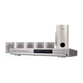
HT-CN410DVH Home Cinema with DVD consisting of HT-
CN410DVH (main unit), CP-CN410F (front speakers), CP-
CN410C
(centre
speakers) and CP-CN410SW (subwoofer).
• In the interests of user-safety (Required by safety
regulations in some countries) the set should be restored to
its original condition and only parts identical to those
specified be used.
CONTENTS
This document has been published to be used for
after sales service only.
The contents are subject to change without notice.
1
HT-CN410DVH
No.S9502HTN410DV
HT-CN410DVH
(for Middle East/ Africa/ Thailand)
speaker),
CP-CN410R
(surround
Page
Advertisement
Table of Contents

Related Manuals for Sharp HT-CN410DVH


Summary of Contents for Sharp HT-CN410DVH
-
Page 1: Table Of Contents
HT-CN410DVH SERVICE MANUAL No.S9502HTN410DV HOME CINEMA WITH DVD HT-CN410DVH MODEL (for Middle East/ Africa/ Thailand) HT-CN410DVH Home Cinema with DVD consisting of HT- CN410DVH (main unit), CP-CN410F (front speakers), CP- CN410C (centre speaker), CP-CN410R (surround speakers) and CP-CN410SW (subwoofer). • In the interests of user-safety (Required by safety... - Page 2 HT-CN410DVH CHAPTER 1. GENERAL DESCRIPTION [1] PRECAUTION FOR USING LEAD-FREE SOLDER 1. Employing lead-free solder "MAIN,DISPLAY,TERMINAL,SWITCH,POWER,JACK,TUNER,DVD,MICVIDEOOUT,CDCHANGERMOTOR(PWBONLY), LED PWB" of this model employs lead-free solder. The LF symbo lindicates lead-free solder,and is attached on the PWB and service manuals.The alphabetical character following LF shows the type of lead-free solder.
-
Page 3: Ac Power Supply Cord
HT-CN410DVH SAFETY PRECAUTION FOR SERVICE MANUAL Precaution to be taken when replacing and servicing the Laser Diode Properties Laser Pickup. Material: AlGaAs/AlGalnP Wavelength: 785 nm/650 nm Emission Duration: continuous The AEL (Accessible Emission Level) of Laser Power Output Laser Output: max. 0.6 mW for this model is specified to be lower than Class 1 Require- ments. -
Page 4: Specifications
HT-CN410DVH SPECIFICATIONS As part of our policy of continuous improvement, SHARP reserves the right to make design and specification changes for product improvement without prior notice. The performance specification figures indicated are nominal values of production units. There may be some deviations from these values in individual units. -
Page 5: Front Speakers
HT-CN410DVH l Front speakers Type Full range speaker system (magnetic shield) 7 cm speaker Maximum input power 30 W Impedance 4 ohms Dimensions Width: 90 mm Height: 110 mm Depth: 100 mm Weight 0.46 kg/each l Surround speakers Type Full range speaker system... -
Page 6: Laser Beam Safety Precautions
HT-CN410DVH LASER BEAM SAFETY PRECAUTIONS This DVD player uses a pickup that emits a laser beam. Do not look directly at the laser beam coming from the pickup or allow it to strike against your skin. The laser beam is emitted from the location shown in the figure. When checking the laser diode, be sure to keep your eyes at least 30cm away from the pickup lens when the diode is turned on. -
Page 7: Standard Notes For Servicing
Soldering Iron Fig. S-1-3 (2) Lift each lead of the flat pack-IC upward one by one, using a sharp pin or wire to which solder will not adhere (iron wire). When heating the pins, use a fine Fig. S-1-1 tip soldering iron or a hot air desoldering machine. - Page 8 HT-CN410DVH (4) Bottom of the flat pack-IC is fixed with glue to the 2. Installation CBA; when removing entire flat pack-IC, first apply (1) Using desoldering braid, remove the solder from the soldering iron to centre of the flat pack-IC and heat foil of each pin of the flat pack-IC on the CBA so you up.
- Page 9 HT-CN410DVH Instructions for Handling Semi-conductors Electrostatic breakdown of the semi-conductors may occur due to a potential difference caused by electrostatic charge during unpacking or repair work. 1. Ground for Human Body Be sure to wear a grounding band (1MΩ) that is properly grounded to remove any static electricity that may be charged on the body.
-
Page 10: Operating Controls And Functions
HT-CN410DVH OPERATING CONTROLS AND FUNCTIONS n Main unit (front panel) On/Stand-by Button 15. DVD Indicator Disc Tray 16. JPEG Indicator Disc Tray Open/Close Button 17. P - SCAN mode Remote Sensor 18. Dolby Digital Signal Indicator Play or Pause Button 19. - Page 11 HT-CN410DVH OPERATING CONTROLS AND FUNCTIONS n Main unit (rear panel) <The bottom of the unit> AC Power Lead Speaker Terminals Audio Output Sockets Audio Input Sockets (TV/AUX) Digital Output Socket (Coaxial) Video Output Socket Component Video Output Socket SCART Output Socket (Audio + Video) AM Loop Aerial Socket 10.
-
Page 12: Remote Control
HT-CN410DVH n Remote Control Remote Control Transmitter On/Stand-by Button Function Button Display Button Dimmer Program Button Language Select Button Frame Advance Button (Step Function) Slow Motion Button 10. Setup Menu Button 11. Cursor Buttons 12. PBC/MENU Button 13. Stop Button 14. -
Page 13: Troubleshooting
HT-CN410DVH TROUBLESHOOTING Severe hum or noise is heard: If you experience any of the following difficulties while using the system, use troubleshooting guide to help you l Check that the speakers and components are con- remedy the problem. Should any problem persist, nected correctly and securely. -
Page 14: Block Diagrams
HT-CN410DVH BLOCK DIAGRAM TV-IN AUX-IN TUNER PACK IC TEA5762H IC TC4052BP IC SAA6588T SWITCH (RDS) TUNER SYSTEM ES680 CS5342 u_COM DVD LOADER SANYO DVD LODER IC ESS6602 DVD RF IC AM5869S DVD PACK DRIVER IC V63111 VFD CONTROL IC AT24C02... - Page 15 HT-CN410DVH Logic HEX Inverter IC SN7404 COAXIAL OUT Y.U.V OUT (OR SCART) ES6809 S-VIDEO u_COM C-VIDEO IC IRC4558 AMPLIFIER IC STA308-A DIGITAL AUDIO PROCESSOR C AT24C02 IC 74HC374 MBM29LV800BA Bilt IN TREBLE BASS EQ RIAL EEPROM I/O PIN EXPAND EPROM...
-
Page 16: Schematic Diagrams / Ic's Pin Voltage
HT-CN410DVH SCHEMATIC DIAGRAMS / IC’S PIN VOLTAGE Standard Notes Notes: 1. Do not use the part number shown on these draw- WARNING ings for ordering. The correct part number is shown in the parts list, and may be slightly different or Many electrical and mechanical parts in this chassis amended since these drawings were prepared. - Page 17 HT-CN410DVH LIST OF CAUTION, NOTES, AND SYMBOLS USED IN THE SCHEMATIC DIAGRAMS ON THE FOLLOWING PAGES: 1. CAUTION: FOR CONTINUED PROTECTION AGAINST FIRE HAZARD, REPLACE ONLY WITH THE SAME TYPE FUSE. 2. CAUTION: Fixed Voltage (or Auto voltage selectable) power supply circuit is used in this unit.
- Page 18 HT-CN410DVH SCHEMATIC DIAGRAM FOR CONTROL PCB RB5503 DP251 R2539 R2540 -27VF R2564 ZD255 BK5V ON/OFF R2560 R2563 4.7K R2502 BK5V BK5V Q2501 R2556 R2501 2SA812 LED-1 C2520 LED-1 LED-2 LED-2 100UF/16V RB204 D2501 1N4148 R2524 1K PMUTE R2528 R2532 R2525 1K...
- Page 19 HT-CN410DVH DP251 DISPLAY 4 1K C2501 5 1K R2526 22K ZD254 C2502 C2510 Grid6 Grid7 Grid8 EARPHONE SECTION Seg20/Grid9 eg19/Grig10 JK5501 FB5507 RB5501 FB5505 eg18/Grid11 FB5506 eg17/Grid12 eg16/Grid13 eg15/Grid14 eg14/Grid15 EARPHONE C5501 C5502 C5507 eg13/Grid16 STANDBY SECTION CN5504 RB5504 TA2507...
- Page 20 HT-CN410DVH SCHEMATIC DIAGRAM FOR POWER PCB When Servicing, pay attention as the area enclosed by this line ( ) is directly connected with AC. REMARKS : SP1CREW-A SP3CREW-A IS 1/4W R04-1-F IS 1/4W 1 OHMRES FUSE SP2CREW-A SP4CREW-A IS 1/6W...
- Page 21 HT-CN410DVH C955 L952 C104P-100V 470P-1KV CN951 FEP16DT C961 +32V D951 1000U 50V -27V R954 C962 R04-22K Jumper C956 CN3P-396 C104P-100V 470P-1KV 1000U 50V JMP30 R06-30K R951 HER104 D952 ZD952 ZD-3V9 C959 D955 1N4148 R962 470P-1KV R958 R06-33K R06-1K2 L951 R06-100...
- Page 22 HT-CN410DVH MAIN CIRCUIT DIAGRAM C224 104 TP231 C225 104 C226 104 C285 C227 104 C286 C228 104 C287 C288 C229 104 C289 C230 104 TP810 C231 104 R811 R812 C233 104 C234 104 R813 C235 104 R814 R854 C236 104...
- Page 23 HT-CN410DVH C301 100P C302 100P TUN_R TUN_L C303 100P C306 102 C305 102 C304 100P C909 104 R854 C910 104 R855 R856 R857 C911 470U/10V R862 C902 C912 470U/16V C913 104 R312 10K C903 104 R31110K C904 10U/16V C313 C914 104...
- Page 24 HT-CN410DVH DB[3] DB[2] ADC_BIAS DB[1] UDAC DB[0] ESS6809 CDAC YDAC VD33 VS33_DAC DB[8] VD33_DAC DB[9] VDAC DB10 DB[10] FDAC DB11 C2009104 R2454K7 DB[11] RSET DB12 DB[12] COMP DB13 DB[13] VREF R2464K7 C279 104 VS33_PLL R2424K7 R272 33 LRCLK R274 33...
- Page 25 HT-CN410DVH ZD202 ZD203 ZD204 R501 C506 R512 TP232 FB201 120 ESS124P TSD2 C508 R2454K7 R511 FB202 120 TP233 ESS121P TSD1 C507 R510 FB203 120 R2464K7 ESS120P TSD0 TP234 C505 R506 ESS119P LRCLK R2424K7 C504 R509 ESS126P BCLK C503 R272 33...
- Page 26 HT-CN410DVH IC’S PIN VOLTAGE IC202 (TE330) Ref.number Mode PLAY STOP IC203 (24C02H) Ref.number Mode PLAY STOP IC204 (NEKS) Ref.number Mode PLAY STOP IC205 (HCT04) Ref.number Mode PLAY STOP PLAY STOP IC209 (74HC374D) Ref.number Mode PLAY STOP PLAY STOP IC301 (4558AM) Ref.number...
- Page 27 HT-CN410DVH IC802 (AM5869) Ref.number Mode PLAY STOP PLAY STOP PLAY STOP IC901 (EL817) Ref.number Mode PLAY -13.1 -12.7 STOP -13.1 -13.1 IC902 (DM0265R) Ref.number Mode PLAY -13.2 -5.5 -12.8 154.1 143.2 143.1 143.1 STOP -13.5 -6.1 -13.1 153.3 145.2 145.2 145.2...
-
Page 28: Waveforms
HT-CN410DVH WAVEFORMS VIDEO OUT S-VIDEO OUT - Y Output Note : S-VIDEO OUT - C Output WF1 ~ WF3 : Power On (Stop) Mode. WF4 ~ WF7 : DVD Test Disc TDV-540A. (Color Bar 75%) COMPONENT VIDEO OUT - Y Output... - Page 29 HT-CN410DVH COMPONENT VIDEO OUT - Pr/Cr Output COMPONENT VIDEO OUT - Pr/Cr Output (Interlace mode) (P-Scan mode) WF10 Audio Left WF11 Audio Right WF12 Rf Signal Note : WF8 ~ WF9 : DVD Test Disc TDV-540A. (Color Bar 75% ) WF10 ~ WF11 : DVD/CD Test Disc 1KHz, 0dB.
- Page 30 HT-CN410DVH -MEMO-...
-
Page 31: Wiring Diagram
HT-CN410DVH WIRING DIAGRAM WIRING SIDE OF POWER PCB COLOUR RD (R) WH (W) WH (P) TABLE BROWN YELLOW BLUE WHITE BLACK WHITE (PINK) FROM MAIN PCB CN902 +12V BK5V ON/OFF BK5V WH (P) -27V WH (P) WH (P) WH (P) - Page 32 HT-CN410DVH WIRING SIDE OF CONTROL PCB TO CONTROL PCB CN5501 WH (P) WH (P) TO MAIN PCB WH (P) CN5001 FROM CONTROL PCB (ON/STANBY) RB5501 WH (P) WH (P) WH (P) WH (P) WH (P) WH (P) WH (P) TO POWER PCB...
- Page 33 HT-CN410DVH WIRING SIDE OF CONTROL PCB Figure 2: WIRING SIDE OF CONTROL PCB (BOTTOM VIEW) (2/2)
- Page 34 HT-CN410DVH WIRING SIDE OF MAIN PC BOARD (TOP VIEW) TO CONTROL PCB TO POWER PCB TO POWER PCB RB204 CN952 CN951 CN204 CN902 CN901 FB902 C911 FB502 D204 ZD901 C558B D202 D203 C908 C531 R901 R402 FB901 R401 C559B C532...
-
Page 35: Component Video Out
HT-CN410DVH FROM CD FROM CONTROL PCB FROM CD TO TUNER TO PICK-UP CHANGER CHANGER PACK RB6501 CN5001 CN301 CN803 C817 CN802 R827 R849 C802 C801 C912 C822 R846 R844 R804 D804 R821 R862 C5017 D204 R817 R830 D203 R815 R814... - Page 36 HT-CN410DVH WIRING SIDE OF MAIN PC BOARD (BOTTOM VIEW) C108 C913 C810 C821 C218 0000 R317 C803 C809 R318 R863 C107 C217 C805 C807 C253 FB216 C130 C2025 C2024 C204 C106 C206 R298 C129 C110 R297 C224 C248 R268 C231...
- Page 37 HT-CN410DVH WIRING SIDE OF MAIN PC BOARD (BOTTOM VIEW) C289 C910 C902 C537 R902 C903 C512 C538 C513 C520 C113 C521 C129 C128 C539 C516 C540 C517 C510 C511 C522 C563 C503 C506 C504 C505 C564 C507 C124 C508 C114...
-
Page 38: Ic Pin Function Descriptions
HT-CN410DVH IC PIN FUNCTION DESCRIPTIONS IC204, Micropower Supply Voltage Supervisor (LM809) Pin Description: RESET Top View Pin Description: PIN(S) NAME DESCRIPTION Negative reference for all signals. RESET Active low reset output. When the sence threshold has been exceeded, the RESET signal will remain active for an additional 140ms(min.) after which it is taken inactive. - Page 39 HT-CN410DVH IC953, Voltage Regulator (TL431) Pin Configuration: Z Package (TO-92) CATHODE ANODE Figure 1: PIN CONFIGURATION OF TL431 Functional Block Diagram: CATHODE ANODE Figure 2: FUNCTIONAL BLOCK DIAGRAM OF TL431...
- Page 40 HT-CN410DVH IC208, High Data Rate Dynamic RAM (K4S641632H) Functional Block Diagram: Data Input Register LDQM Bank Select 4M x 4 / 2M x 8 / 1M x 16 4M x 4 / 2M x 8 / 1M x 16 4M x 4 / 2M x 8 / 1M x 16...
- Page 41 HT-CN410DVH IC208, High Data Rate Dynamic RAM (K4S641632H) Pin Description: Name Input Function System clock Active on the positive going edge to sample all inputs. Disables or enables device operation by masking or enabling all inputs except Chip select CLK, CKE and DQM Masks system clock to freeze operation from the next clock cycle.
- Page 42 HT-CN410DVH IC 902, Power Switching Motor (FSDM 0265 RN) Pin Definitions: Pin Number Pin Name Pin Function Description Sense FET source terminal on primary side and internal control ground. Positive supply voltage input. Although connected to an auxiliary transformer winding, current is supplied from pin 5 (Vstr) via an internal switch during startup (see Internal Block Diagram section).
- Page 43 HT-CN410DVH IC901, Optical Sensor (EL-817) Pin Configuration: Pin No. And Internal Connection Diagram 1. Anode 3. Emitter 2. Cathode 4. Collector IC951, Dual Operational Amplifier (NJM4558) Equivalent Circuit (as Shown): OUTPUT - INPUT + INPUT Connection Diagram: PIN FUNCTION (Top View) 1.
- Page 44 HT-CN410DVH IC952, SMPS Controller (KA7500C) Internal Block Diagram: OUTPUT CONTROL OSCILLATOR DEAD TIME 1.2V CONTROL COMP EA (+) BAND GAP EA (-) REFERENCE 0.7MA EA (+) EA (-) COMP INPUT Figure 5: KA7500C BLOCK DIAGRAM IC209, Octal D-Type Flip-Flop (74HC/HCT374) Pin Description: PIN NO.
- Page 45 HT-CN410DVH IC207, High Speed Flash Memory (MX29LV160BBTC-70G) Pin Description: SYMBOL PIN NAME A0~A19 Address Input Q0~Q14 Data Input/Output Q15/A-1 Q15(Word mode)/LSB addr(Byte mode) Chip Enable Input Write Enable Input BYTE Word/Byte Selection input RESET Hardware Reset Pin/Sector Protect Unlock Output Enable Input...
- Page 46 HT-CN410DVH IC207, High Speed Flash Memory (MX29LV160BBTC-70G) Block Diagram: WRITE CONTROL PROGRAM/ERASE STATE INPUT HIGH VOLTAGE MACHINE LOGIC RESET (WSM) STATE REGISTER ADDRESS FLASH ARRAY LATCH ARRAY A0-A19 SOURCE COMMAND DATA BUFFER Y-PASS GATE DECODER SENSE DATA COMMAND AMPLIFIER DATA LATCH...
- Page 47 HT-CN410DVH IC205, HEX Inverters (74HCT04) SN54HCT04...JORW PACKAGE SN74HCT04...D, N, OR PW PACKAGE (TOP VIEW) V CC Logic Diagram (Positive Logic): IC202, Wide-Band Video Switch (TS5V330DBQR) Pin Configuration: Pin Description: Pin Name Description Description Pin Name Pin Name Description S1, S2...
- Page 48 HT-CN410DVH IC201, Programmable Multimedia and DSP Processor (ES6809FADF) ES6809 Pinout Diagram: The device pinout for the ES6809 is shown in Figure 1. AVSS VD33PLL SPDIF_IN SPDIF_OUT LOE# RPBC VD33 TEBC REFD IN_M AVDD3 AVSS DVCC LCS3# IDSEL AMPSTBY LCS2# FGIN...
- Page 49 HT-CN410DVH IC201, Programmable Multimedia and DSP Processor (ES6809PADF) ES6809 Pin Description: Names Pin Numbers Definitions 1, 11, 20, 36, 45, 53, 63, 80, 97, VD33 I/O power supply. 122, 130, 156, 182, 197 AUX0 Host control 0. AUX3 Auxiliary port 3.
- Page 50 HT-CN410DVH IC201, Programmable Multimedia and DSP Processor (ES6809PADF) Table 1 ES6809 Pin Description (Continued): Names Pin Numbers Definitions VDAC VideoDAC output. Refer to description and matrix for UDAC pin 115. YUV6 YUV pixel 6 ouput data. PIXOUT6 CCIR656 output pixel 6.
- Page 51 HT-CN410DVH IC201, Programmable Multimedia and DSP Processor (ES6809PADF) Table 1 ES6809 Pin Description (Continued): Names Pin Numbers Definitions Audio transmit serial data port 2. TSD2 Audio left channel 3 out. AOUT_O3L Audio transmit serial data port 3. TSD3 Audio right channel 3 out.
- Page 52 HT-CN410DVH IC201, Programmable Multimedia and DSP Processor (ES6809PADF) Table 1 ES6809 Pin Description (Continued): Names Pin Numbers Definitions 3.3V analog power for flash. AVDD3 Analog ground for flash. AVSS 1.8V power for flash. DVCC DVD-RAM header position index 1. DVD-RAM detected signal of ID area.
- Page 53 HT-CN410DVH IC203, EEPROM (AT24C02N-10SU-2.7) Table 1 EEPROM Pin Configuration Pin Name Function A0 - A2 Address Inputs 8-lead SOIC Serial Data Serial Clock Input Write Protect No Connect Ground Power Supply IC801, DVD Servo (ES6602SF) ES6602 PINOUT 48 47 46 45 44 43 42 41 40 39 38 37 36 35 34 33...
- Page 54 HT-CN410DVH IC801, DVD Servo (ES6602SF) ES6602 PIN DESCRIPTION Names Pin Numbers Definitions DVDRFP, DVDRFN Differential RF signal attenuator inputs. AC coupled photo detector interface input for the differential phase A2, B2, C2, D2 detector (DPD) from the main beam photo matrix.
- Page 55 HT-CN410DVH Table 1 ES6602 Pin Description List (Continued) Names Pin Numbers Definitions RF block and serial port ground. FNN, FNP 52, 53 Differential outputs of equalizer/filter. Differential analog input to the RF single-end output buffer and full DIP, DIN 54, 55 wave rectifier.
- Page 56 HT-CN410DVH IC303, 192 kHz Multi-bit audio A/D Converter (CS5342) Pin Name Pin Description Mode Selection (Input) - Determines the operational mode of the device. MCLK Master Clock (Input) - Clock source for the delta-sigma modulator and digital filters. Logic Power (Input) - Positive power for the digital input/output.
- Page 57 HT-CN410DVH IC5002, Headphone Driver with Mute (APA 3541-TRL) Function Pin Description Pin Name Function Description Out A A channel output pin Mute Chip disable control input, low active and high for normal operating Input A A channel input terminal Power ground pin...
- Page 58 HT-CN410DVH IC501, Multi Channel Digital Audio (STA308A) Pin Connection (Top view) OUT2_A OUT2_B SDI_78 OUT3_A SDI_56 OUT3_B SDI_34 OUT4_A SDI_12 OUT4_B LRCKI OUT5_A BICKI OUT5_B RESET OUT6_A PLLB OUT6_B STA308APINCON Table 1. Pin Function Name Description Pad Type Master Volume Override/...
- Page 59 HT-CN410DVH IC501, Multi Channel Digital Audio (STA308A) Table 1. Pin Function (Continued) Name Description Pad Type OUT8A PWM Channel 8 Output A 3.3V Capable TTL 2mA Output Buffer OUT7B PWM Channel 7 Output B 3.3V Capable TTL 2mA Output Buffer...
- Page 60 HT-CN410DVH IC502 & IC504, Power Half Bridge (STA518) Table 1. Pin Function Description GND-SUB Substrate ground 35 ; 36 Vcc Sign Signal Positive supply Vcc1A Positive supply Vcc1B Positive supply Vcc2A Positive supply Vcc2B Positive supply GND1A Negative Supply GND1B...
- Page 61 HT-CN410DVH IC502 & IC504, Power Half Bridge (STA518) Table 2. Functional Pin Status Pin Name Pin No Logical value IC-Status FAULT Fault detected (Short circuit, or Thermal) FAULT* Normal Operation TRI-STATE All powers in Hi-Z state TRI-STATE Normal Operation PWRDN...
- Page 62 HT-CN410DVH IC301, IC401, IC5001 Dual Wide Bandwidth Operational Amplifiers (RC4558) Pin Configuration: Pin Description: Function Pin No. Output A Input A Input A Input B Input B Output B IC302, Channel Multiplexer (D4052BM) Pin Configuration: IN/OUT IN/OUT OUT/IN D4052BM OUT/IN...
-
Page 63: Pin Configuration
HT-CN410DVH IC251, VFD Driver (TP6311) Pin Configuration: 41 40 SG20/GR9 SG19/GR10 DOUT SG18/GR11 SG17/GR12 SG16/GR13 SG15/GR14 SG14/GR15 SG13/GR16 Block Diagram: SG1/KS1 SG2/KS2 Control SG3/KS3 SG4/KS4 Serial SG5/KS5 DOUT Data SG6/KS6 Interface Display Memory SG7/KS7 (20 bits X 16 words) Segment... - Page 64 HT-CN410DVH IC251, VFD Driver (PT6311) Pin Description: Pin Name Function Pin No. SW1 to SW4 General Purpose Input pins 1 to 4 Data Output Pin (N-Channel, Open-Drain) DOUT This pin outputs serial data at the falling edge of the shift clock (starting from the...
-
Page 65: Fl Display
HT-CN410DVH FL DISPLAY 92LKLV00003410 PATTERN: P-SCAN R-D-S DIGITAL AUDIO PL II SACD JPEG S V C D MP3 STEREO PRESET TITLE PROG SLP RND REP 1 SHUFF GRID ASSIGNMENT: P-SCAN R-D-S DIGITAL AUDIO PL II SACD JPEG S V C D MP3... - Page 66 HT-CN410DVH FL DISPLAY PIN CONNECTION Pin No. 9 10 11 12 13 14 16-19 20 21 22 23 24 25 26 27 28 29 30 31 32 33 34 35 36 37 38 39 F1 F2 NP NP 1G 2G 3G 4G 5G 6G 7G 8G 9G 10G...
-
Page 67: Parts Guide
HT-CN410DVH PARTS GUIDE HOME CINEMA WITH DVD HT-CN410DVH MODEL CONTENTS [1] INTEGRATED CIRCUITS [11] OTHER CIRCUITRY PARTS [2] TRANSISTORS [12] DVD MECHANISM PARTS [3] DIODES [13] P.W.B. ASSEMBLY (Replacement Items) [4] VIBRATORS/CRYSTALS CABINET PARTS (MAIN UNIT) [5] RESONATOR ACCESSORIES PARTS... - Page 68 HT-CN410DVH PRICE PART PARTS CODE DESCRIPTION RANK MARK RANK [1] INTEGRATED CIRCUITS IC201 92LRCI00680902 IC 208PIN ES6809FADF PQFP ESS LF IC202 92LRCI05033002 IC 16PIN TS5V330DBQR QSOP TI QUAD WIDE-BANDWIDTH VIDEO SWITCH IC203 92LRCI02400202 GP IC 8PIN AT24C02N-10SU-2.7 SOIC ATMEL EEPROM...
- Page 69 HT-CN410DVH PRICE PART PARTS CODE DESCRIPTION RANK MARK RANK [4] VIBRATORS/CRYSTALS XL201 92LJQC02200060 GP CRYSTAL 27.0000MHz HC-49US +/-20PPML=12.7MM [5] RESONATOR XL2501 92LJRN14000110 GP Resonator MURATA CSB 455EB (455KHZ) [6] TRANSFORMER(Non Replacement Parts) T901 92LTSA10001014 GP SW Transformer ERL-28 / 34 100W Boulder Pitch = 30mm...
- Page 70 HT-CN410DVH PRICE PART PARTS CODE DESCRIPTION RANK MARK RANK [8] CAPACITORS C276 92LPXL41037010 GP Chip Capacitor 100pF 50V 5% 0603 Type NPO Capacitor C278 92LPXL41037050 GP Chip Capacitor 15pF 50V 5% 0603 Type NPO Capacitor C279 92LPXL45647040 GP Chip Capacitor 0.1uF 50V 10% 0603 Type X7R Capacitor...
- Page 71 HT-CN410DVH PRICE PART PARTS CODE DESCRIPTION RANK MARK RANK [8] CAPACITORS C806,C807 92LPXL45647040 GP Chip Capacitor 0.1uF 50V 10% 0603 Type X7R Capacitor C808,C809 92LPXL45647040 GP Chip Capacitor 0.1uF 50V 10% 0603 Type X7R Capacitor C810 92LPXL45647040 GP Chip Capacitor 0.1uF 50V 10% 0603 Type X7R Capacitor...
- Page 72 HT-CN410DVH PRICE PART PARTS CODE DESCRIPTION RANK MARK RANK [8] CAPACITORS C2009 92LPXL45647040 GP Chip Capacitor 0.1uF 50V 10% 0603 Type X7R Capacitor C2010 92LPXL45647040 GP Chip Capacitor 0.1uF 50V 10% 0603 Type X7R Capacitor C2011 92LPXL45647040 GP Chip Capacitor 0.1uF 50V 10% 0603 Type X7R Capacitor...
- Page 73 HT-CN410DVH PRICE PART PARTS CODE DESCRIPTION RANK MARK RANK [9] RESISTORS R268 92LQCF01503002 GP Resistor 1K Ohm 1/10W 5% 0603 SMT Type R269 92LQCF01503047 GP Chip Res 4.7K Ohm 1/10W 5% 0603 SMT Type R26A 92LQCF04501090 GP Chip Resistor 6.2 Ohm 1/4 W 5% 1206 SMT Type...
- Page 74 HT-CN410DVH PRICE PART PARTS CODE DESCRIPTION RANK MARK RANK [9] RESISTORS R849 92LQCF01503050 GP Chip Res 1M Ohm 1/10W 5% 0603 SMT Type R850 92LQCF01503040 GP Chip Res 100K Ohm 1/10W 5% 0603 SMT Type R851 92LQCF01503043 GP Chip Res 4.3K Ohm 1/10W 5% 0603 SMT Type...
- Page 75 HT-CN410DVH PRICE PART PARTS CODE DESCRIPTION RANK MARK RANK [9] RESISTORS R2532~R2535 92LQCF01503000 GP Chip Resistor 0 Ohm 1/10 W 5% 0603 SMT Type R2536,R2537 92LQCF01503047 GP Chip Resistor 4.7K Ohm 1/10 W 5% 0603 SMT Type R2538 92LQCF01503012 GP Chip Resistor 1.2K Ohm 1/10 W 5% 0603 SMT Type...
- Page 76 HT-CN410DVH PRICE PART PARTS CODE DESCRIPTION RANK MARK RANK CABINET PARTS (MAIN UNIT) 92LBPL20000601 SHARP BADGE 92LBPF10603201 FRONT PANEL 92LBRF10003303 LEG CUSHION 92LBPN10024401 FL WINDOW 92LBPK10508701 VOLUME KNOB 92LBPK10607201 POWER KNOB 92LIVE30100303 SUPPORT CUSHION 92LBPK11607201 OPEN/CLOSE KNOB 92LBPK12607201 OPERATION KNOB...
- Page 77 HT-CN410DVH PRICE PART PARTS CODE DESCRIPTION RANK MARK RANK SURROUND SPEAKER BOX PARTS (CP-CN410R) 92LNSR54005281 SCREW 92LIVE52000202 CUSHION 92LASW50300894 SPEAKER LEAD (RIGHT) 92LASW50300893 SPEAKER LEAD (LEFT) 92LANF20000403 BACK CAB ASSEMBLY 92LNSR54006221 SCREW 92LYLB811004SR SPEC LABLE (RIGHT) 92LYLB811004SL SPEC LABLE (LEFT)
- Page 78 HT-CN410DVH EXPLODED VIEW MAIN UNIT HT-CN410DVH 601x5 601x2 601x2 604x7 PWB-A1 PWB-A3 207x4 PWB-A2 601x4 Figure 1: CABINET EXPLODED VIEW...
- Page 79 HT-CN410DVH MAIN UNIT HT-CN410DVH 601x2 604x10 HEAT SINK A HEAT SINK C 601x4 HEAT SINK B 231x4 601x4 PWB-C TUNER PACK PWB-B 605x4 Figure 2: CABINET EXPLODED VIEW...
- Page 80 HT-CN410DVH SATELLITE SPEAKER SYSTEM CP-CN410F CP-CN410C CP-CN410R 902x4 SP1(CENTRE) SP1,2 906x4 TABLE 1 SPEAKER CHANNEL LEAD COLOR RIGHT RED + BLACK FRONT LEFT WHITE + BLACK 2 CENTRE GREEN + BLACK RIGHT GREY + BLACK 3 SURROUND LEFT BLUE + BLACK...
- Page 81 HT-CN410DVH SUBWOOFER CP-CN410SW VIOLET BLACK 907x4 VIOLET 909x4 SPEAKER Figure 2: SUBWOOFER BOX PARTS...
- Page 82 HT-CN410DVH -MEMO-...
- Page 83 HT-CN410DVH -MEMO-...
- Page 84 HT-CN410DVH © COPYRIGHT 2005 BY SHARP CORPORATION ALL RIGHTS RESERVED. No part of this publication may be reproduced, stored in a retrieval system, or transmitted in any form or by any means, electronic, mechanical, photocopying, recording, or otherwise, without prior written permission of the publisher.