Pioneer DV-F727 Service Manual
Hide thumbs
Also See for DV-F727:
- Operating instructions manual (80 pages) ,
- Brochure & specs (16 pages)
Table of Contents
Advertisement
FILE-TYPE DVD PLAYER
DV-F727
DV-F07
THIS MANUAL IS APPLICABLE TO THE FOLLOWING MODEL(S) AND TYPE(S).
Model
Type
DV-F727
KU
KC
KU/RC
KU/CA
-
CONTENTS
1. SAFETY INFORMATION ....................................... 2
2. EXPLODED VIEWS AND PARTS LIST ................. 3
4. PCB CONNECTION DIAGRAM ........................... 39
5. PCB PARTS LIST ................................................ 55
6. ADJUSTMENT ..................................................... 62
PIONEER CORPORATION
PIONEER ELECTRONICS SERVICE, INC. P.O. Box 1760, Long Beach, CA 90801-1760, U.S.A.
PIONEER ELECTRONIC (EUROPE) N.V. Haven 1087, Keetberglaan 1, 9120 Melsele, Belgium
PIONEER ELECTRONICS ASIACENTRE PTE. LTD. 253 Alexandra Road, #04-01, Singapore 159936
c
PIONEER CORPORATION 1999
PLA Y MODE
RANDOM
DISPLA Y
ST ANDBY
ST ANDBY / ON
Power Requirement
DV-F07
-
AC120V
-
AC120V
-
AC120V
AC120V
4-1, Meguro 1-chome, Meguro-ku, Tokyo 153-8654, Japan
DIRECT CUSTOM
PUSH ENTER
DISC/
CHARA
1
2
3
4
5
6
7
8
9
TEXT
AUDIO/VIDEO
UPDA TE
INPUT
SEARCH
10
CLEAR
CLEAR
FILE-TYPE DVD MECHANISM
SINGLE LOADER
OPEN/
ACCESS
PLA Y
CLOSE
KEYBOARD
/MOUSE
Region No.
1
1
3
1
7. GENERAL INFORMATION .................................. 66
7.1 DIAGNOSIS ................................................... 66
7.1.1 TEST MODE SCREEN DISPLAY ............. 66
7.1.2 TROUBLE SHOOTING ............................ 68
7.1.3 OPERATION FLOW CHART .................... 69
7.1.4 ERROR CODE ......................................... 70
7.1.5 INTERFACE CONNECTOR ..................... 74
7.1.6 DISASSEMBLY ........................................ 77
MECHANISM FAILURE ............................ 79
7.2 PARTS ........................................................... 80
7.2.1 IC ............................................................. 80
7.2.2 DISPLAY .................................................. 95
8. PANEL FACILITIES AND SPECIFICATIONS ....... 96
ORDER NO.
RRV2236
Remarks
T - IZE DEC. 1999 Printed in Japan
Advertisement
Table of Contents

Related Manuals for Pioneer DV-F727


Summary of Contents for Pioneer DV-F727
-
Page 1: Table Of Contents
PIONEER CORPORATION 4-1, Meguro 1-chome, Meguro-ku, Tokyo 153-8654, Japan PIONEER ELECTRONICS SERVICE, INC. P.O. Box 1760, Long Beach, CA 90801-1760, U.S.A. PIONEER ELECTRONIC (EUROPE) N.V. Haven 1087, Keetberglaan 1, 9120 Melsele, Belgium PIONEER ELECTRONICS ASIACENTRE PTE. LTD. 253 Alexandra Road, #04-01, Singapore 159936 PIONEER CORPORATION 1999 T –... -
Page 2: Safety Information
The use of a substitute replacement component which does Leakage 0.5mA current Device not have the same safety characteristics as the PIONEER tester under recommended replacement one, shown in the parts list in test this Service Manual, may create shock, fire, or other hazards. -
Page 3: Exploded Views And Parts List
See Contrast table (2) Battery Cover VNK4423 Audio Cord (L = 1.5m) VDE1033 (2) CONTRAST TABLE DV-F727/KU, KC, KU/RC and DV-F07/KU/CA are constructed the same except for the following : Part No. Mark No. Symbol and Description Remarks DV-F727 DV-F727... - Page 4 DV-F727, DV-F07 2.2 EXTERIOR SECTION (1/2) DV-F07 DV-F07 Only DV-F727 Only Only DV-F727/KU DV-F07/KU/CA Only DV-F727 Only DV-F07 Only Note ∗1 Part of Center Pole ∗1 DV-F07 Only DV-F727/KU/RC Refer to Only "2.3 EXTERIOR SECTION (2/2)". DV-F07 Only from PS2B Assy...
- Page 5 Screw IPZ30P080FMC PCB Support Cushion VEC2079 Region Label See Contrast table (2) (2) CONTRAST TABLE DV-F727/KU, KC, KU/RC and DV-F07/KU/CA are constructed the same except for the following : Part No. Mark No. Symbol and Description Remarks DV-F727 DV-F727 DV-F727...
- Page 6 DV-F727, DV-F07 2.3 EXTERIOR SECTION (2/2) Note ∗3 : Froil 397 (for Service) : GYA1001 Note ∗4 : Refer to Ha Narl PN955R (for Service) : GEM1016 "2.4 DISC RACK SECTION". ∗4 ∗4 Note ∗2 (Screw Cover) Part of Trans Cover (No.10) ∗3...
- Page 7 Dispersion Sheet VEC2113 Rear Base See Contrast table (2) Center Pole 301 PNW2792 (2) CONTRAST TABLE DV-F727/KU, KC, KU/RC and DV-F07/KU/CA are constructed the same except for the following : Part No. Mark No. Symbol and Description Remarks DV-F727 DV-F727...
- Page 8 DV-F727, DV-F07 2.4 DISC RACK SECTION Note ∗3 : Froil 397 (for Service) : GYA1001 Note ∗4 : Ha Narl PN955R (for Service) : GEM1016 ∗4 ∗3 ∗3 ∗3 ∗3 ∗3 ∗3 ∗3 ∗3...
- Page 9 DV-F727, DV-F07 DISC RACK SECTION PARTS LIST Mark No. Description Part No. Refer to SSRB Assy VWG2113 "2.6 TRAVERSE MECHANISM ASSY". SEMB Assy VWG2114 LOMB Assy VWG2115 LOSB Assy VWG2116 RADB Assy VWG2117 PHOB Assy VWG2118 VOLB Assy VWG2123 Clamp Spring...
-
Page 10: Front Panel Section
Enter Button PAC1883 Display Window PAM1782 Screw PPZ30P100FMC Screw PPZ30P050FMC (2) CONTRAST TABLE DV-F727/KU, KC, KU/RC and DV-F07/KU/CA are constructed the same except for the following : Part No. Mark No. Symbol and Description Remarks DV-F727 DV-F727 DV-F727 DV-F07 /KU/RC... -
Page 11: Traverse Mechanism Assy
DV-F727, DV-F07 2.6 TRAVERSE MECHANISM ASSY • Top View TRAVERSE MECHANISM ASSY PARTS LIST Mark No. Description Part No. Mark No. Description Part No. SMEB Assy VWG2048 Hook VNL1770 FGSB Assy VWG2009 FFC Holder VNL1802 Motor VXM1079 Mechanism Base VNL1806... -
Page 12: Block Diagram And Schematic Diagram
DV-F727, DV-F07 3. BLOCK DIAGRAM AND SCHEMATIC DIAGRAM 3.1 BLOCK DIAGRAM 33M 16M DVDM ASSY (24P) (24P) CN120 SPDL MOTOR OEIC RF IC SD0-SD7 DSPRF 7,6, 7,6, B1-B4 57-60 DECODER IC101 63-66 MY CHIP LA9701M F_RTN SREQ TRKG F_DRV IC701... - Page 13 DV-F727, DV-F07 (26P) (26P) 36/16M CN110 CN201 IC22 YCBR0-7 M + 6V (Y0-Y7) TC7WH74FU 95-98, +12V MPEG2 100-103 149,150, DECODER 36/16M +12V 152-155, MITUBISHI 158,159 POWER AV-1 SUPPLY IC801 CLOCK GENERATOR DOUT0 M65773AFP IC21 ASSY +3.3V CN101 CY2081SL-655 LIVE AC IN...
- Page 14 DOSB ASSY DOMB ASSY (VWG2122) (VWG2121) J632 J631 J632 LOMB ASSY 1/2, (VWG2115) LOSB ASSY AVJB ASSY (VWG2116) (DV-F727 : VWV1719) (DV-F07 : VWV1720) LEAF SW J652 J651 VOLB ASSY (VWG2123) MDRB ASSY SSRB ASSY PHOB ASSY (VWG2113) (VWG2127) (VWG2118)
- Page 15 : SELECT DRIVE SIGNAL ROUTE (DV-F07 : VWS1396) (SP) (SP) POWER SUPPLY ASSY (VWR1317) AC POWER CORD ADG7024 (SL) PICKUP ASSY (VWY1055) KEYB ASSY (VWG2120) VQEB ASSY (VWV1669) FLKY ASSY (DV-F727/KU, KC : VWG2126) (DV-F727/KU/RC : VWG2191) PS2B ASSY (DV-F07 : VWG2119) (VWG2125)
- Page 16 DV-F727, DV-F07 3.3 DVDM ASSY (1/4) (DVD) (DVD) CN201 VKN1324 CN110 VKN1479 (CD) (CD) RF IC CN120 VKN1464 CN1030 VKN1471 SPINDLE & FTS (SP) DRIVER (SP)
- Page 17 DV-F727, DV-F07 DVDM ASSY (DV-F727 : VWS1386) (DV-F07 : VWS1396) : The power supply is shown with the marked box. : RF SIGNAL ROUTE : ROM DATA SIGNAL ROUTE : FOCUS SERVO LOOP LINE : TRACKING SERVO LOOP LINE FOR CHECKER...
- Page 18 DV-F727, DV-F07 3.4 DVDM ASSY (2/4) DVDM ASSY (DV-F727 : VWS1386) (DV-F07 : VWS1396) 3→5 CONVERTER 5→3 CONVERTER IC603 IC604 VYW1668 TC55V1001FAF8 DV-F07 ONLY CN106 VKN1299 CN107 3/4,4/4 VKN1575 1/4,3/4 SH1 BASE ASIC (SL)
- Page 19 DV-F727, DV-F07 : The power supply is shown with the marked box. : AUDIO SIGNAL ROUTE : ROM DATA SIGNAL ROUTE : DOOR DRIVE SIGNAL ROUTE (SL) : SELECT DRIVE SIGNAL ROUTE IC702 MN414800CSJ-07 4M DRAM (MY CHIP ES2) DVD ENCODER 3→5 CONVERTER...
- Page 20 DV-F727, DV-F07 3.5 DVDM ASSY (3/4) DV-F07 ONLY 16M SDRAM IC801 M65773AFP MPEG2 ENCODER 3→5 CONVERTER...
- Page 21 DV-F727, DV-F07 DVDM ASSY (DV-F727 : VWS1386) : AUDIO SIGNAL ROUTE (DV-F07 : VWS1396) : ROM DATA SIGNAL ROUTE : VIDEO SIGNAL ROUTE : Y SIGNAL ROUTE : C SIGNAL ROUTE FOR SERVO DSP CLOCK GEN. BLOCK CN101...
- Page 22 DV-F727, DV-F07 3.6 DVDM ASSY (4/4) DVDM ASSY (DV-F727 : VWS1386) (DV-F07 : VWS1396) CN921 VKN1471 (SL) 5→3 CONVERTER CN302 CN903 VKN1497 CN901 : AUDIO SIGNAL ROUTE : VIDEO SIGNAL ROUTE 3→5 CONVERTER : Y SIGNAL ROUTE : C SIGNAL ROUTE...
- Page 23 DV-F727, DV-F07...
- Page 24 DV-F727, DV-F07 3.7 VQEB ASSY VQEB ASSY (VWV1669) (6 ch, DNR) VIDEO ENCODER...
- Page 25 DV-F727, DV-F07 : The power supply is shown with the marked box. : ROM DATA SIGNAL ROUTE : VIDEO SIGNAL ROUTE : Y SIGNAL ROUTE : C SIGNAL ROUTE CN802 Q531, Q532, Q541, Q542, Q551, Q552 : 2PB709A (QR) F102 : VTF1155...
- Page 26 DV-F727, DV-F07 3.8 AVJB ASSY (1/2) AVJB ASSY (DV-F727 : VWV1719) (DV-F07 : VWV1720) IC201 DV-F727 : PCM1716E DV-F07 : PE8001A CN101 VKN1190 CN905 DV-F727 ONLY DV-F07 ONLY Hi-Bit...
- Page 27 DV-F727, DV-F07 : AUDIO SIGNAL ROUTE : The power supply is shown with the marked box. JA201 DV-F727 : VKB1132 DV-F07 : VKB1133...
- Page 28 DV-F727, DV-F07 3.9 AVJB ASSY (2/2) CN501 VKN1191 (V/P (V/P (C/P (C/P CN901 CN502 VKN1183 (V/P CN902 (C/P JA504 (2/2) DV-F727 : VKB1134 DV-F07 : VKB1135 (V/P (C/P (V/P (C/P CN503 (2/2) VIDEO DV-F727 : AKP7020 DV-F07 : AKP7023 SELECTOR...
- Page 29 DV-F727, DV-F07 AVJB ASSY (DV-F727 : VWV1719) : VIDEO/PB SIGNAL ROUTE (DV-F07 : VWV1720) : Y SIGNAL ROUTE (C/P : C/PR SIGNAL ROUTE : The power supply is shown with the marked box. JA504 (1/2) DV-F727 : VKB1134 DV-F07 : VKB1135...
- Page 30 DV-F727, DV-F07 3.10 MSJB ASSY MSJB ASSY (DV-F727 : VWG2131) CN904 AKN1028 (DV-F07 : VWG2128) CN905 AKN1028 CN903 VKN1211 CN702 MSCHK, SLCHK Normal : Low Plug in : High JA906 RKN1004 JA907 RKN1004 CN901 VKN1215 JA908 CN903 PKN1005 CN902 VKN1211...
- Page 31 DV-F727, DV-F07 : The power supply is shown with the marked box. : DIGITAL AUDIO SIGNAL ROUTE JA902 GP1F32T JA901 DV-F727 : VKB1077 DV-F07 : VKB1074 JA903 DV-F727 : VKB1077 DV-F07 : VKB1074...
- Page 32 DV-F727, DV-F07 3.11 MDRB ASSY MDRB ASSY (VWG2127) CN306 52147-0310 J1601 CN303 VKN1184 CN301 VKN1188 CN304 52147-0410 CN302 VKN1188 CN305 52147-0510 CN307 52147-0910...
- Page 33 DV-F727, DV-F07 3.12 232B ASSY (DV-F07 ONLY) 232B ASSY (VWG2129) CN401 VKN1183 CN106...
- Page 34 DV-F727, DV-F07 3.13 FLKY, KEYB and PS2B ASSYS FLKY ASSY (DV-F727/KU, KC : VWG2126) (DV-F727/KU/RC : VWG2191) CN602 (DV-F07 : VWG2119) CN701 VKN1191 DV-F727 /KU/RC ONLY...
- Page 35 DV-F727, DV-F07 MSCHK, SLCHK CN702 Normal : Low : The power supply is shown with the marked box. Plug in : High VKN1183 KEYB ASSY (VWG2120) CN903 CN1202 CN703 52045-1145 52045-1145 FLKY ASSY S701 : STYANDBY/ON PS2B ASSY (VWG2125) S702 : ACCESS...
- Page 36 DV-F727, DV-F07 3.14 POWER SUPPLY ASSY POWER SUPPLY ASSY (VWR1317) T101 TRANS D201 R110 R102 D105 D202 R115 C108 R103 L102 D102 D101 D203 R112 R113 C107 D106 C106 D103 D104 Q103 D110 Q101 C111 PC102 R104 R114 R101 D109...
- Page 37 DV-F727, DV-F07 NOTE OF SPARE PARTS IN POWER SUPPLY (SYPS) ASSY • In case of repairing, use the described parts only to prevent an accident. • Please write the red mark on the board when the primary section of POWER SUPPLY (SYPS) Assy is repaired.
- Page 38 DV-F727, DV-F07 WAVEFORMS Note : The encircled numbers denote measuring point in the schematic diagram. Measurement condition : No. 1 to 4 and 6 to 11 : Disc MA1, Title 1-chp 1 No. 5 : CD, ABEX-784 Track 1 No. 12 to 14 : MJK1, Title 1-chp 4 or T2-1 No.
-
Page 39: Pcb Connection Diagram
DV-F727, DV-F07 4. PCB CONNECTION DIAGRAM NOTE FOR PCB DIAGRAMS : 1. Part numbers in PCB diagrams match those in the schematic 3. The parts mounted on this PCB include all necessary parts for diagrams. several destinations. 2. A comparison between the main parts of PCB and schematic For further information for respective destinations, be sure to diagrams is shown below. - Page 40 DV-F727, DV-F07 4.1 FGSB, SMEB, SSRB, SEMB, LOMB, LOSB, RADB, PHOB,DOMB, DOSB, VOLB and LEDB ASSYS FGSB ASSY CN303 SMEB R101 ASSY CARRIAGE SPINDLE MOTOR (VNP1661-B) MOTOR (VNP1695-A) CN307 SSRB ASSY SEMB ASSY SELECT MOTOR (VNP1727-A) (VNP1727-A) RADB Q603 Q604...
- Page 41 DV-F727, DV-F07 SEMB ASSY SSRB ASSY (VNP1727-A) (VNP1727-A) RADB ASSY VOLB ASSY (VNP1727-A) PHOB ASSY LEDB ASSY (VNP1727-A) (VNP1726-A) DOMB ASSY (VNP1726-A) LOMB ASSY LOSB ASSY DOSB ASSY (VNP1727-A) (VNP1727-A) (VNP1726-A) SIDE B (VNP1726-A) C D E F G H I J K L...
- Page 42 DV-F727, DV-F07 • This PCB is a four-layered board. 4.2 DVDM ASSY CN401 CN101 CN501 DVDM ASSY IC23 IC26 IC31 Q810 Q808 Q812 IC25 IC54 Q809 Q807 Q811 IC21 IC801 VR851 IC807 VC21 IC22 IC806 IC903 IC261 IC303 PICKUP ASSY...
- Page 43 DV-F727, DV-F07 • This PCB is a four-layered board. DVDM ASSY IC905 IC803 IC27 IC805 IC802 IC73 CN101 IC201 IC701 IC231 Q542 Q179 IC608 Q106 Q105 Q237 IC299 Q113 Q543 Q106 IC904 Q114 IC609 IC611 IC612 Q101 IC751 Q103 IC792...
- Page 44 DV-F727, DV-F07 4.3 AVJB ASSY AVJB ASSY Q120 IC203 IC206 IC202 IC201 IC241 IC150 Q150 Q588 IC501 IC502 Q589 Q592 Q591 Q591 Q587 Q586 (VNP1725-A) CN901 CN905 CN902 SIDE A...
- Page 45 DV-F727, DV-F07 AVJB ASSY Q201 Q202 Q257 Q277 Q281 Q151 Q582 Q584 Q585 Q583 Q561 Q581 (VNP1725-A) SIDE B...
- Page 46 DV-F727, DV-F07 4.4 VQEB ASSY VQEB ASSY SIDE A (VNP1696-B) VR102 VR101 Q551 Q541 IC106 Q531 IC103 IC105 Q521 Q511 Q501 VQEB ASSY SIDE B (VNP1696-B) CN802 Q502 Q512 IC102 Q522 IC104 Q532 Q542 Q552...
- Page 47 DV-F727, DV-F07 4.5 MSJB ASSY MSJB ASSY CN702 CN903 CN502 (VNP1726-A) Q987 SIDE A MSJB ASSY (VNP1726-A) IC921 IC922 IC931 IC901 Q981 SIDE B...
- Page 48 DV-F727, DV-F07 4.6 MDRB ASSY MDRB ASSY MDRB ASSY J631 J651 J1601 Q301 CN921 CN1030 Q302 Q303 IC301 CN202 VR301 J601 (VNP1726-A) SIDE A SIDE B...
- Page 49 DV-F727, DV-F07 4.7 232B ASSY (DV-F07 ONLY) 232B ASSY IC401 CN106 (VNP1726-A) SIDE A 232B ASSY (VNP1726-A) SIDE B...
- Page 50 DV-F727, DV-F07 4.8 FLKY, KEYB and PS2B ASSYS CN903 CN602 FLKY ASSY (VNP1726-A) IC701 IC702 SIDE A...
- Page 51 DV-F727, DV-F07 KEYB ASSY IC1251 IC1201 (VNP1726-A) PS2B ASSY (VNP1726-A)
- Page 52 DV-F727, DV-F07 KEYB ASSY (VNP1726-A) PS2B ASSY (VNP1726-A)
- Page 53 DV-F727, DV-F07 FLKY ASSY (VNP1726-A) Q702 Q701 SIDE B...
- Page 54 DV-F727, DV-F07 4.9 POWER SUPPLY ASSY POWER SUPPLY ASSY AC IN Q103 Q101 Q122 Q102 Q121 IC201 IC301 VR201 VR301 VR202 IC203 IC202 Q301 CN110 SIDE A...
-
Page 55: Pcb Parts List
DV-F727, DV-F07 Mark No. Description Part No. Mark No. Description Part No. 5. PCB PARTS LIST • NOTES: Parts marked by "NSP" are generally unavailable because they are not in our Master Spare Parts List. • mark found on some component parts indicates the importance of the safety factor of the part. - Page 56 R754 RS1/10S622J RS1/10S622J RS1/10S103J R755 Not used RS1/10S623J Not used R756 RS1/10S0R0J RS1/10S473J RS1/10S0R0J PCB PARTS LIST FOR DV-F727/KU UNLESS OTHERWISE NOTED Mark No. Description Part No. Mark No. Description Part No. RESISTORS FGSB ASSY All Resistors RD1/4PU SEMICONDUCTOR OTHERS...
- Page 57 DV-F727, DV-F07 Mark No. Description Part No. Mark No. Description Part No. LOSB ASSY LEDB ASSY SWITCH SEMICONDUCTORS LEAF SWITCH VSK1011 D1611 HZU6.2B D1601 NSPB500-9235 OTHERS RESISTORS 3P CABLE HOLDER 51048-0300 All Resistors RS1/10S OTHERS RADB ASSY 3P CABLE HOLDER...
- Page 58 DV-F727, DV-F07 Mark No. Description Part No. Mark No. Description Part No. CAPACITORS RESISTORS C612 CCSRCH100D50 R123 (39Ω×4) ACN7047 C123,C145,C21,C282,C617 CCSRCH101J50 R715,R716 (47Ω×4) ACN7077 CCSRCH120J50 R531,R543,R545,R613 (10kΩ×4) DCN1094 C126,C333 CCSRCH150J50 R648,R649,R706,R707,R748 DCN1094 C206,C210,C211 CCSRCH151J50 (10kΩ×4) C322 CCSRCH180J50 R751 (10kΩ×4) DCN1094...
- Page 59 DV-F727, DV-F07 Mark No. Description Part No. Mark No. Description Part No. C550,C552 CEAT471M6R3 CAPACITORS C150 CKSQYB103K50 C130 CCSRCH102J50 C520-C522,C561,C585 CKSQYB104K25 C101,C120 CEV101M16 C587 CKSQYB222K50 C110-C119,C121-C126,C150 CKSRYB104K16 C583 CKSQYB473K50 C160,C532,C542,C552 CKSRYB104K16 C201,C202 (2.2µF) VCG1031 C101,C103,C120,C123,C151 CKSQYF104Z25 C153,C204,C205,C208,C209 CKSQYF104Z25 RESISTORS C214,C215,C230,C233,C234...
- Page 60 DV-F727, DV-F07 Mark No. Description Part No. Mark No. Description Part No. JA901,JA903 1P PIN JACK VKB1077 FLKY ASSY CN902,CN903 VKN1211 7P FFC CONNECTOR SEMICONDUCTORS CN901 11P FFC CONNECTOR VKN1215 SCREW TERMINAL VNE1948 IC701 PE5144A IC702 S-806D Q701-Q704 PDTC124EK D701...
- Page 61 DV-F727, DV-F07 Mark No. Description Part No. Mark No. Description Part No. PS2B ASSY FILTERS F801-F804 EMI FILTER VTH1009 CAPACITORS C801-C804 CCSQCH101J50 C813,C814 CKSQYF104Z25 RESISTORS All Resistors RS1/10S OTHERS JA801 MINI DIN 6P SOCKET RKN1038 CN801 7P FFC CONNECTOR VKN1211...
-
Page 62: Adjustment
DV-F727, DV-F07 6. ADJUSTMENT 6.1 ADJUSTMENT ITEMS AND LOCATION Note : When the Traverse mechanism adjustment is not properly adjusted, jitter, error rate and play ability are defective. The noise may come out by the case. Adjustment Points (PCB Part) -
Page 63: Necessary Adjustment Points
DV-F727, DV-F07 6.3 NECESSARY ADJUSTMENT POINTS When Adjustment Points EXCHANGE PCB ASSY Mechanical Exchange board point VOLB ASSY, SSRB ASSY, RADB ASSY, PHOB ASSY Electric point Mechanical Exchange board point DVDM ASSY Electric point Note : is adjusted already. 6.4 ELECTRICAL ADJUSTMENT Master Clock Adjustment •... - Page 64 DV-F727, DV-F07 Disc-select Rotation Adjustment DC power supply Connection Diagram for Adjustment –8V VOLB ASSY Digital multimeter (Peak hold circuit) VR601 KN601 Player INPUT OUTPUT (Under Base) Adjustment Procedure 1. Connect all equipment as shown in the diagram. 2. Turn on the power (Normal mode) and put the test disc in the No. 1 disc slot.
- Page 65 DV-F727, DV-F07 Simple Adjustment of Disc Detection Connection Diagram for Adjustment Stopped 22 - NOV - 1999 16 46 CH2 = 200mV 2 s/d DC P*10 Peak value is OK with 950 - 1100mV. Go arround (except for single loader)
-
Page 66: General Information
DV-F727, DV-F07 7. GENERAL INFORMATION 7.1 DIAGNOSIS 7.1.1 TEST MODE SCREEN DISPLAY Consecutive double-OSD display is supported during test mode. The screen is composed 10 lines with a maximum of 32 characters per line. It can't be used with the debugging display mode together. - Page 67 DV-F727, DV-F07 (10) Output video system [V – ∗ ∗ ∗ ∗] (19) The part number of the flash ROM and system controller [∗ ∗ ∗ ∗ ∗ ∗ / ∗ ∗ ∗ ∗ ∗ ∗ ∗ ] NTSC system...
-
Page 68: Trouble Shooting
DV-F727, DV-F07 7.1.2 TROUBLE SHOOTING • No Power ON • FL is not turned ON • FL indication is unusual START • Blow out fuse (F101) of the primary side. Power ON • Varister (Z101) on the POWER SUPPLY Assy is damaged. -
Page 69: Operation Flowchart
DV-F727, DV-F07 7.1.3 OPERATION FLOWCHART From power-on till the end of initialization (Power ON) Initialization of memory Setup of the destination and the type of player according to the data received from the microprocessor for the FL display. Process of closing the hood... -
Page 70: Error Code
DV-F727, DV-F07 7.1.4 ERROR CODE l l o c i f ) . l ) . l l l o n i l u l i l l a t ' d t I ( l l a ) . l ) . - Page 71 DV-F727, DV-F07 ± r i f r i f t s i t ' n t i s v i f r i f t ' n v i f 7 " " 3 t i s 7 " " 3...
- Page 72 DV-F727, DV-F07 u l i l i a u l i u l i l l o l l o l l o f i c µ . ) µ f i c c i f c i f f i c...
- Page 73 DV-F727, DV-F07...
-
Page 74: Interface Connector
DV-F727, DV-F07 7.1.5 INTERFACE CONNECTOR • Communication control • Specifications of Interface The protocol system is based on a system in which the computer Signal level : RS-232C level gives commands and the player returns statuses. The communication Data format... - Page 75 DV-F727, DV-F07 • List of Commands − f i c − f i c − − − − − y l i l l i t t c i − . y l − − − − − l t i t...
-
Page 76: Normal Operation
DV-F727, DV-F07 • Error List f i c , e l e l i y l t r i f . e l • Notes Normal operation • Some operations in Search mode are prohibited for some discs. In such a case, an error is not generated when the mode is specified, but an error is generated when execution of the SE command is attempted. -
Page 77: Disassembly
DV-F727, DV-F07 7.1.6 DISASSEMBLY Bonnet and Side Panle L, R DVDM Assy DV-F07 ONLY VQEB Assy ×4 ×3 ×2 DVDM Assy DV-F727 ×2 ONLY ×2 Slit ×4 DV-F07 ONLY Diagnosis • Remove the VQEB Assy when diagnosing the circuit under the VQEB Assy of DVDM Assy. - Page 78 DV-F727, DV-F07 ×5 Center Pole 301 Clamper Holder Float Base Traverse Mechanism Assy ×3 Unhook Clamp Clamp pole Spring Open Front Hood Arm Assy ×3 Traverse Mechanism Assy ×4 PU FFC ×4 Float Rubber A Disc Guard Remove Link part.
-
Page 79: About Service In The Mechanism Failure
DV-F727, DV-F07 7.1.7 ABOUT SERVICE IN THE MECHANISM FAILURE Gear Holder Assy and Disc Rack • Draw two discs of CD • Pin of A portion in the figure deviates from the groove Perform the steps of the Traverse Mechanism Assy. -
Page 80: Parts
DV-727, DV-F07 7.2 PARTS 7.2.1 IC • The information shown in the list is basic information and may not correspond exactly to that shown in the schematic diagrams. • List of IC LC78652W, PD3410A, VYW1668, M65773AFP, PM0023AF, CY2081SL-655 LC78652W (DVDM ASSY : IC201) •... - Page 81 DV-F727, DV-F07 • Pin Function t f i − − l l i t t i y t i t l i − − − − a i l t l i −...
- Page 82 DV-727, DV-F07 r r i t i r − − − − l a i t f i − − l l i l i f − t l i f t l i f t l i f − −...
- Page 83 DV-F727, DV-F07 PD3410A (DVDM ASSY : IC601) • System Control IC • Pin Function − − − − − c t i − , c i - t l − − , c i - t l → l a i...
- Page 84 DV-727, DV-F07 − − − − − − c t i c t i − c t i c t i c t i c t i − c t i − − l l o − −...
- Page 85 DV-F727, DV-F07 − t i s d i l t i s − − − l l o l a i e l l l a i e l l − e l l − − −...
- Page 86 DV-727, DV-F07 − − − − − − −...
- Page 87 DV-F727, DV-F07 VYW1668 (DVDM ASSY : IC603) • 16M bit Flash Memory IC • Block Diagram - DQ 29-36,38-45 RY/BY RY/BY Buffer Erase Voltage Input/Output Generator Buffers State Control BYTE RESET Command Program Voltage Register Generator Chip Enable Output Enable...
- Page 88 DV-727, DV-F07 M65773AFP (DVDM ASSY : IC801) • MPEG2 Decoder IC • Block Diagram 16M bit SDRAM SDRAM Bit Streem Descrambler Controller Bit Streem Input Interface Video Decoder Sub-picture Decoder Internal Display Processor Special Playback 16M DRAM Processor Host Video Output Host CPU Video Output Interface...
- Page 89 DV-F727, DV-F07 − y l l n i l − n i l − n i l n i l...
- Page 90 DV-727, DV-F07 n i l n i l n i l n i l n i l n i l n i l n i l n i l n i l n i l n i l n i l n i l n i l n i l...
- Page 91 DV-F727, DV-F07 PM0023AF (VQEB ASSY : IC101) • VQE4 IC • Block Diagram MPU Interface with Macrovision Configuration Register Closed Caption VBID MPEG2 Sync and Timing Signal Generator Video Generator Decoder MPEG2 Video Processing Engine 6 ch Input 6 ch Video 75 Ω...
- Page 92 DV-727, DV-F07 e l l − . ) r v i t y t i c i t . ) r v i t y t i − − l l u − − l l u − l l u l l u −...
- Page 93 DV-F727, DV-F07 − − v i t y t i c i t v i t y t i − − − − − t s i − t s i − − Ω t s i Ω t s i µ...
- Page 94 DV-727, DV-F07 Ω t s i > µ t i c Ω t s i Ω t s i Ω t s i µ t i c Ω t s i > µ t i c Ω t s i t s i −...
-
Page 95: Display
DV-F727, DV-F07 7.2.2 DISPLAY VAW1052 (FLKY ASSY : V701) • FL Display Pin Assignment Pin Connection Pin No. Connection NP NP 13G 12G 11G 10G 9G 8G Pin No. Connection 6G 5G 4G 3G 2G 1G NX NX NX NX NX NX NX Pin No. -
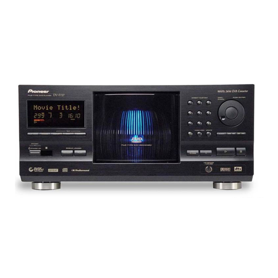
Page 96: Panel Facilities And Specifications
DV-F727, DV-F07 8. PANEL FACILITIES AND SPECIFICATIONS 8.1 PANEL FACILITIES Front Panel F I L E - T Y P E D V D P L A Y E R DIRECT CUSTOM PUSH ENTER DISC/ CHARA AUDIO/VIDEO UPDA TE TEXT... -
Page 97: Display Window
DV-F727, DV-F07 ¡ ¢ (forward) button OPEN/CLOSE button Press to advance to chapters/tracks. Press and hold to perform Press to open and close the hood. fast-forward scanning. When using the front panel to edit input text, use to move the position of the cursor. - Page 98 DV-F727, DV-F07 Character display LAST MEMORY indicator Displays text information already recorded on the disc such as Indicates the Last Memory location is registered in memory for CD TEXT or DVD text, and also text manually input into the the DVD currently playing.
-
Page 99: Remote Control Unit
DV-F727, DV-F07 Remote Control Unit All of the command buttons on the remote control glow in the dark (Buttons indicated with * are used for menu operation.) for easy control of the player even in the dark. Hold the unit under a light for optimal results. - Page 100 DV-F727, DV-F07 ¡ Number buttons (1-9, 0, +10)* Dial mode indicator Use to select a disc, perform direct title and chapter/track Lights red when the player is in the Jog Mode and green when searches, and to input numerical values.
-
Page 101: Rear Panel
Use to connect this player to another component bearing the Connect the VIDEO IN jack to the video output of another DV- Pioneer Î mark. This lets you control this unit as though it F727 player or another component with video output capability. -
Page 102: Specifications
AA (R6P) dry cell batteries ............. 2 Weight (DV-F07) ..........9.7 kg (21 lbs. 6 oz.) Audio cord ..................1 Dimensions (DV-F727) ....420 (W) x 434 (D) x 193 (H) mm Video cord ..................1 (W) x 17 (D) x 7 (H) in.)