Panasonic CQ-C1323NW Service Manual
Hide thumbs
Also See for CQ-C1323NW:
- Operating instructions (4 pages) ,
- Operating instructions (2 pages)
Table of Contents
Advertisement
Specifications*
General
Power Supply
Tone Controls
Current Consumption
Maximum Power Output
Suitable Speaker Impedance
Pre-Amp Output Voltage
Output Impedance
FM Stereo Radio
Frequency Range
Usable Sensitivity
AM Radio
Frequency Range
DC 12V (11V - 16V),
Test Voltage 14.4V
Negative Ground
Bass ; ±12dB at 100Hz
Treble ; ±12dB at 10kHz
Less than 2.2A (CD play mode,
0.5W×4ch)
50W×4ch (at 1kHz, Vol. Max.)
4-8Ω
2.5V (CD play mode; 1kHz, 0dB)
200Ω
87.5 - 108MHz
11.0dBf (1.25µV, 75Ω)
531 - 1,602kHz
AUTOMOTIVE AFTERMARKET
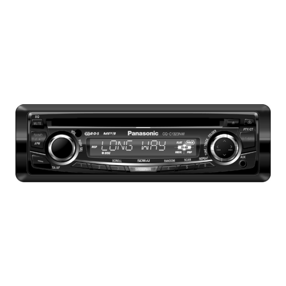
CQ-C1323NW
Removable Front Panel CD Player /
Receiver
Usable Sensitivity
RDS
RDS Sensitivity
CD Player
Sampling Frequency
Pick-Up Type
Light Source
Wavelength
Frequency Response
Signal to Noise Ratio
Dimensions**
Weight**
* Specifications and the design are subject to possible modification
without notice due to improvements.
** Dimensions and Weight shown are approximate.
© 2005 Matsushita Electric Industrial Co., Ltd. All
rights
reserved.
distribution is a violation of law.
Order No. ACED051217C8
28dB/µV (25µV, S/N 20dB)
22dB/µV
8 times oversampling
Astigma 3-beam
Semiconductor Laser
780nm
20Hz to 20,000Hz (±1dB)
96dB
178×50×155mm
1.4kg
Unauthorized
copying
and
Advertisement
Table of Contents

Related Manuals for Panasonic CQ-C1323NW


Summary of Contents for Panasonic CQ-C1323NW
-
Page 1: Specifications
Order No. ACED051217C8 AUTOMOTIVE AFTERMARKET CQ-C1323NW Removable Front Panel CD Player / Receiver Specifications* General Usable Sensitivity 28dB/µV (25µV, S/N 20dB) Power Supply DC 12V (11V - 16V), Test Voltage 14.4V RDS Sensitivity 22dB/µV Negative Ground Tone Controls Bass ; ±12dB at 100Hz CD Player Treble ;... -
Page 2: Table Of Contents
CQ-C1323NW CONTENTS Page Page 1 ABOUT LEAD FREE SOLDER (PbF) 11 PACKAGE AND IC BLOCK DIAGRAM 2 FEATUERS 12 REPLACEMENT PARTS LIST 3 REPLACEING THE FUSE 13 EXPLODED VIEW (Unit) 4 MAINTENANCE 14 CD PLAYER MECHANICAL PARTS LIST 5 NOTES... -
Page 3: Dimensions
CQ-C1323NW 7 DIMENSIONS... -
Page 4: Wiring Connection
CQ-C1323NW 8 WIRING CONNECTION... -
Page 5: Block Diagram
CQ-C1323NW 9 BLOCK DIAGRAM... -
Page 6: Terminals Description
CQ-C1323NW 10 TERMINALS DESCRIPTION 10.1. Main Block IC601 : LC7237849D10 Part No. Part Name & I/O(V) FM( AM(V CD(V Description Part No. Part Name & I/O(V) FM( AM(V CD(V Description 51 AMP_MUTE Amp mute 5.19 5.19 X’tal 2.54 2.53 52 N.C. - Page 7 CQ-C1323NW Part No. Part Name & I/O(V) FM( AM(V CD(V Ref. Part No. Part Name & Description Description DVDD18 VDD capacitor connection port 1.83 for digital circuit. 98 EO1 phase comparison 2.02 0 MONI0 Monitor port0. error output MONI1 Monitor port1.
- Page 8 CQ-C1323NW 10.2. Display Block IC901 : YEAMLC75854W Pin No. Port Descriptions No connection 5-39 SEG5-39 LCD segment 40-43 COM1-4 LCD common 44-49 KS1-6 Key data output 50-54 KI1-5 Key data input TEST (Connecting to ground) +5V power supply VDD1 Ground through capacitor...
-
Page 9: Package And Ic Block Diagram
CQ-C1323NW 11 PACKAGE AND IC BLOCK DIAGRAM 11.1. Main Block PA51:J3CCBC000010 IC271 : C1EA00000041... - Page 10 CQ-C1323NW IC401 : C1BB00001088 IC701 : C0DAZHF00004...
- Page 11 CQ-C1323NW IC251 : C1BB00000804...
- Page 12 CQ-C1323NW IC551:C1BB00000960...
-
Page 13: Replacement Parts List
CQ-C1323NW 12 REPLACEMENT PARTS LIST Ref. Part No. Part Name & Description Remarks D713 YEAD1N4005ST Silicon Diode D714 YEAD1N4005ST Silicon Diode D715 YEAD1N4005ST Silicon Diode D716 YEAD1N4005ST Silicon Diode D717 YEAD1N4005ST Silicon Diode D719 YEAD1N4005ST Silicon Diode D720 YEAD1N4005ST Silicon Diode... - Page 14 CQ-C1323NW Ref. Part No. Part Name & Description Remarks Ref. Part No. Part Name & Description Remarks C311 F2A1H2R2A407 Electrolytic 2.2pF 50WV C631 F1J1H101A532 Ceramic 100pF 50WV C312 ECQV1H224JL2 Plastic Film 0.22MFD 50WV C632 F1J1H101A532 Ceramic 100pF 50WV C313 F1J1H222A733...
- Page 15 CQ-C1323NW Ref. Part No. Part Name & Description Remarks Ref. Part No. Part Name & Description Remarks ERJ8GX0R00V Chip 0 ohms 1/8W R472 D0GF103JA014 Chip 10k ohms 1/8W ERJ8GX0R00V Chip 0 ohms 1/8W R501 D0GD331JA017 Chip 330 ohms 1/10W ERJ8GX0R00V...
- Page 16 CQ-C1323NW Ref. Part No. Part Name & Description Remarks Ref. Part No. Part Name & Description Remarks R660 D0GD122JA017 Chip 1.2k ohms 1/10W SW903 K0H1BA000445 Tack Swich R661 D0AZ104JA008 Chip 100k ohms 1/6W SW904 K0H1BA000445 Tack Swich R681 D0GD271JA017 Chip 270 ohms 1/10W...
- Page 17 CQ-C1323NW Ref. Part No. Part Name & Description Remarks YEJT034C019N Screw(CUP TIGHT 3X12) T(3-C) XTB3+8FFZ Screw T(3-C) YJS064C002FN Screw T(3-C) XTB26+8GFN Screw T(3-C) YFA084C063CA Rear Plate T(3-C) YFC034C002CA ESC Holder T(2-C) YFX054C074CA Spring (HOOK) T(2-C) YEFX9991682B Release Hook T(2-C) YEFS02302...
-
Page 18: Exploded View (Unit)
CQ-C1323NW 13 EXPLODED VIEW (Unit) -
Page 19: Cd Player Mechanical Parts List
CQ-C1323NW 14 CD PLAYER MECHANICAL PARTS LIST Ref. Part No. Part Name & Description Remarks 3032 10 39 SP WIRE MN N(D-2) 3032 10 13 WIRE CLAMPER M N(C-2); N(C-3); N(D-4); N(E-3) 3032 10 28 WIRE TUBE SPM N(D-2) 3032 10 29... -
Page 20: Exploded View (Cd Deck)
CQ-C1323NW 15 EXPLODED VIEW (CD Deck) -
Page 21: Wiring Diagram
CQ-C1323NW 16 WIRING DIAGRAM 16.1. Main Block-1 [E-4C286][TOP VIEW] CQ-C1303H/C1303U/C1301NE/C1303NW/C1313NE/C1313NW CQ-C1323NE/C1323NW/C1333U/C1333W MAIN PCB... - Page 22 CQ-C1323NW 16.2. Main Block-2 [E-4C286][BOTTOM VIEW] CQ-C1303H/C1303U/C1301NE/C1303NW/C1313NE/C1313NW CQ-C1323NE/C1323NW/C1333U/C1333W MAIN PCB...
- Page 23 CQ-C1323NW 16.3. Display Block [E-4C287][TOP VIEW] [E-4C287][BOTTOM VIEW] CQ-C1313NE/C1313NW/C1323NE/C1323NW/C1333U/C1333W CQ-C1303H/C1303U/C1303NE/C1303NW DISPLAY PCB...
- Page 24 CQ-C1323NW 16.4. CD Interface Block [E-4C288][BOTTOM VIEW] CQ-C1103U/W/H/D CQ-C1333U/W CQ-C1303U/W/H/D/NE/NW CQ-C1313NE/NW CQ-C1323NE/NW CD INTERFACE PCB...
-
Page 25: Schematic Diagram-1
CQ-C1323NW 17 SCHEMATIC DIAGRAM-1 17.1. Main Block E-4C286 0.12 0.26 0.36 13.06 12.36 0.13 5.12 4.57 4.52 5.23 4.57 4.53 4.57 5.21 4.57 4.52 4.53 0.68 4.52 4.53 4.56 5.17 4.53 5.17 4.55 5.21 5.23 0.89 8.22 8.21 8.11 8.22 8.16... - Page 26 THIS PAGE IS JUST FOR THE PAGE LAYOUT USE ONLY.
-
Page 27: Schematic Diagram-2
CQ-C1323NW 18 SCHEMATIC DIAGRAM-2 18.1. Display Block... - Page 28 CQ-C1323NW 18.2. CD Interface Block...
-
Page 29: Schematic Diagram For Printing With A4 Size
CQ-C1323NW 19 SCHEMATIC DIAGRAM for printing with A4 size 19.1. Main Block (Left Side) 0.12 0.26 0.36 4.57 4.52 5.23 4.57 4.53 4.57 5.21 4.52 4.57 4.53 0.68 4.52 4.53 4.56 5.17 4.53 5.17 4.55 8.22 8.21 8.11 8.22 8.16 8.18... - Page 30 CQ-C1323NW 19.2. Main Block (Right Side) E-4C286 13.06 12.36 0.13 5.12 4.57 4.52 4.57 4.53 4.57 4.52 4.57 4.53 0.68 4.52 4.53 4.56 5.17 4.53 5.17 4.55 5.21 5.23 0.89 3.25 3.25 1.08 1.83 0.08 3.29 1.23 1.84 1.04 1.65 0.88...