Table of Contents
Advertisement
Quick Links
This service manual provides a variety of service
information. It contains the mechanical structure of
the DVD-ROM Drive together with mechanical
adjustments and the electronic circuits in schematic
• 5.25" Half-height size built-in type DVD-ROM Drive
• Enhanced IDE (ATAPI) bus interface (SFF-8090v3 rev.1.00 and SFF-8020i rev.2.6) Standard 2.54mm pitch
bus connector for non-shielded type cable
• Ultra DMA 33 support
• Authentication function support
• 16 mode output for CD audio
• Software Volume Control via ATAPI Mode Select Command
• Headphones output volume control for CD-DA
• PC99 compatible
• Tray type loading with emergency eject
• Low self vibration and low acoustic noise
• Dust-free chassis
• Installation posture : Horizontal / Vertical
• MTBF : 125,000 POH
• <DVD-ROM>
1) Single layered disc : 6.7 to 16X max. Full CAV, data transfer : 22.1 Mbytes/s max.
Dual layered disc
Video disc (w/CSS) : 3.3 to 8X max. Full CAV, data transfer : 11.1 Mbytes/s max.
2) High speed access : Random access time 120ms typical (Single layered disc)
3) Read compatible for both 4.7Gbytes/side and 3.9Gbytes/side DVD-R disc.
4) Read compatible for DVD-RW (Ver.1.0 & 1.1)/DVD+RW disc
• <CD-ROM>
1) 21 to 48X max. Full CAV, data transfer : 7.2 Mbytes/s max.
2) High speed access : Random access time 100ms typical
3) CD-R, CD-RW, CD Extra, CD TEXT disc read compatible
4) Addressing Methode 2 for fixed length Packet supported (CD-R Orange Book Part2)
5) CD-DA (Digital Audio) data output through the IDE bus
6) Embedded error correction EDC & ECC for Mode 1 & Mode 2 Form 1
7) MPC 3 compatible
8) Max. 48X D.A.E. Speed (Correspond to Max. 48X Write CD-R/RW drive)
• <DVD-RAM>
1) Read compatible for both 4.7Gbytes/side and 2.6Gbytes/side DVD-RAM disc
2) 2.6Gbytes/side DVD-RAM 2X speed ZCLV : 2,770Mbytes/s typ.
3) 4.7Gbytes/side DVD-RAM 2X speed ZCLV : 2,770Mbytes/s typ.
4) High speed access : 210 ms typical (1/3 stroke)
INTRODUCTION
GENERAL FEATURES
:
5 to 12X max. Full CAV, data transfer : 16.6 Mbytes/s max.
form. This DVD-ROM Drive was manufactured and
assembled under our strict quality control standards
and meets or exceeds industry specifications and
standards.
3
Advertisement
Table of Contents

Related Manuals for LG GDR-8161B


Summary of Contents for LG GDR-8161B
-
Page 1: General Features
INTRODUCTION This service manual provides a variety of service form. This DVD-ROM Drive was manufactured and information. It contains the mechanical structure of assembled under our strict quality control standards the DVD-ROM Drive together with mechanical and meets or exceeds industry specifications and adjustments and the electronic circuits in schematic standards. -
Page 2: Specifications
SPECIFICATIONS 1. SUPPORTED SYSTEM • IBM Compatible Pentium 133MHz or Above (with PIO mode 4, TX chip set recommended) 2. SUPPORTED OS • MS-DOS (Ver 3.1 or Higher) • OS/2 Warp (Ver 3.0) • Windows 3.1/95/98/2000/ME/XP • Solaris (Ver 2.4 or Higher) •... -
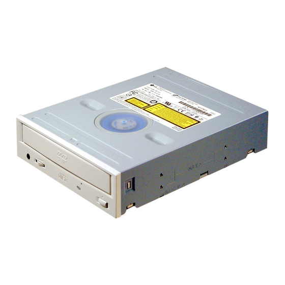
Page 3: Location Of Customer Controls
LOCATION OF CUSTOMER CONTROLS FRONT VIEW R O M R O M R O M R O M COMPACT Headphone Jack Emergency Eject Hole Standard (3.5mm) stereo jack for listening to the Insert a paper clip here to eject the drawer manually or ″... - Page 4 EXPLODED VIEW PBM00 (MAIN C.B.A)
-
Page 5: Pick-Up Unit
INTERNAL STRUCTURE OF THE PICK-UP 1. Structure of the Pick-Up PICK-UP UNIT Q001 CN18 VCC CN06 VC (Vref). CN05 GND-PD CN10 A/a CN09 B/b CN15 C/c CN14 D/d CN17 E1/e2+f2 CN16 E2/e3+f3 CN07 F1/e1+f1 CN08 F2/e4+f4 CN11 CD/DVD SW DVD= 0V C D=+5V CN13 RF+ CN12 RF-... - Page 6 For CD For DVD SF-HD66 VRCD VRDVD CD: Hi DVD: Lo IC201 IC101 Q102,Q104 Monitor resister SW circuit 1. Structure of the Pick-up SF-HD66 is consist of monitor diode for DVD laser and CD laser. When DVD laser is ON, PG101 20 Pin is need to connect GND for getting monitor voltage.(PG101 22 pin). When CD laser is ON, PG101 19 Pin is need to connect GND for getting monitor voltage.(PG101 22 pin).
- Page 7 2. Structure of the Photo Diode (CD) (As seen from light receiving side) 1) Focus Error Signal –> (A + C) - (B+C) • In case of CD Disc This signal is generated in RF AMP IC (IC101) and controls the pick-up’s up and down to focus on CD Disc.
- Page 8 3. Structure of the Photo Diode (DVD-ROM) (As seen from light receiving side) 1) Focus Error Signal –> (a+c) - (b+d) • In case of DVD Disc This signal is generated in RF AMP IC (IC101) and controls the pick-up’s up and down to focus on DVD Disc.
- Page 9 4. Structure of the Photo Diode (DVD-RAM) (As seen from light receiving side) 1) Focus Error Signal –> {(a+c) - (b+d)} - 1.17 x {(e ) - (e • In case of DVD Disc This signal is generated in RF AMP IC (IC101) and controls the pick-up’s up and down to focus on DVD Disc.
-
Page 10: Description Of Circuit
DESCRIPTION OF CIRCUIT 1. ALPC (Automatic laser power control) 1-1. ALPC Circuit Constitution Dual laser power control for DVD and CD are provided. The laser ON for DVD or CD can be selected by LDSEL and the lasers ON/OFF are controlled by LDOFF . Laser power for DVD and CD can be programmable by LDPWR 0,1 IC101 DVD-RAM 4.7G : about 0.77V... - Page 11 2. RF Amplifier Circuit IC101 IC201 RFINP For boost 0.5Vpp Slicer NARF 0.5Vpp RFINN For fc AGCG AGCO 1.65V RF Amplifier Circuit 2-1. Input stage The differential RF signal for data read from pick up may feed into IC401 pin 47 and pin 48. 2-2.
- Page 12 3. SERVO SIGNAL 3-1. FOCUSING ERROR (FE) x1.17 S-Curve : about 1.65Vpp S-Center : 1.65V FESEL 0, 1 IC201 Offset Add. Detect circuit Amplitude 1.65V FBAL 3.3V Tracking 1.65V Focusing Error circuit FE for DVD-ROM,CD are made from 4D(A,B,C,D). FE S-curve amplitude is detected from IC201 109 pin and FE gain is controlled by register “FEG” to keep 1.65V amplitude.
- Page 13 3-2. AS (ALL SUM) IC101 IC201 FOCUS ON : about 2.5V FOCUS OFF : about 1.65V Detect Amplitude 1.65V 1.65V AS circuit AS(All sum) signal is obtained from low pass filter and FOK is made from AS signal in IC201. This FOK signal is used to check servo status.
- Page 14 3-3. TRACKING ERROR (TE) 3-3-1. TE for DVD-ROM (DPD) IC201 3.3V TBAL Offset Add circuit H.P.F Balance Detect H.P.F. H.P.F 1.65V TESEL H.P.F. 1.65V 1.65Vpp Center Voltage = 1.65V Tracking error Circuit TE signal for DVD-ROM is made by DPD (Differential Phase Detect) method. TE signal is made that add voltage obtain form phase differnece of front spot A, D to voltage obtain two phase difference of rear spot B, C.
- Page 15 3-3-2. TE for DVD-RAM, CD (DPP) IC101 DVD-RAM 2.6G, 4.7G : x1.17 CD : x1.9 IC201 DPPG 1.65Vpp. Center voltage =1.65V Offset Bal. TESEL Detect 1.65V 1.65V Tracking error Circuit TE signal for DVD-RAM 2.6G,4.7G is programmable by DPP. In case of DVD-RAM,sub spot(sub beam) is amplified by 1.17times and 1.9times in case of CD and add into main spot(main beam).
- Page 16 3-4. LNSC (LENS CENTER SIGNAL) LNSC Circuit LENSC signal is used as error signal for tracking servo. This signal is used only for long seek (about 1000 track seek). This signal make lens fixed at detector center.
- Page 17 3-5. FOCUS SERVO IC201 IC101 Parallel digital compensator IC301 (Drive IC) Amplitude Detect 1.65V DC Voltage Focus search Generator Algorithm Focus servo system Focus servo system is used to find focus ON point and to trace focus actuator into focus point using parallel digital compensator.
- Page 18 3-6. TRACKING SERVO SYSTEM IC201 IC301 Parallel (Drive IC) digital compensator Lens control LNSC 3.3V Sled Compensator Quantity of Lens shift Controlled by prediction and lens shift quantity. SIN1 IC301 (Drive IC) SIN2 To control stepping motor Tracking servo system Tracking servo is used to follow trace center of detector with TE signal and to control stepping motor.
- Page 19 IC201 Compensator IC201 (Tracking cross) Track number counter 1.65V 1.65V Tracking cross for seek control TKC is digital signal of “H”, “L” which is compared to TE signal in center of amplitude. TKC is used to make constant track cross speed and jumped track count in case of multi-jump (number of track: about less than 1000 track)in IC201.
- Page 20 4. About DVD-RAM 2.6G, 4.7G signal User data section CAPA section User data section PG101 IC101 RFDIF IC202 IDGATE IC202 DTRD IC202 VFOSHORT IC101 Signal timing for DVD-RAM 2.6G, 4.7G...
- Page 21 IC101 IC201 IDGATE Generator Comparator RFDIF Only Seek DTRD Generator VFOSHORT SLICER Generator NARF Decoder 124 123 DTRD IDGATE VFOSHORT DVD-RAM 2.6G, 4.7G system DVD-RAM 2.6G, 4.7G have CAPA(Complementary Allocated Pit Address) differnt from DVD-ROM. CAPA is consist of same pit like DVD-ROM disk,that’s why even blank disk has it. CAPA has PID(Physical ID) which shows address on disk.
-
Page 22: Description Of Data Processing
DESCRIPTION OF DATA PROCESSING 1. Data Processing Flow... -
Page 23: Copy Protection And Regional Code Management Block
2. Copy Protection and Regional Code Management Block Block Diagram Change the "KEY" HOST DVD PLAYER MN103S37 (EMPEG2 DECODER) Scrambled MPEG Data KEY Management Control Brief Process 1. Regional Code for DVD Disc – DVD-ROM drive transfers the regional code of the control data to host by the command of host, the DVD player of host reads the regional code, and plays title in the case of allowed regional code only. -
Page 24: About Prevention The Dvd-Rom From To Be Copy
3. About Prevention the DVD-ROM from to be copy A data is able to encode and record in the disc, if a copyright holder wants to prevent the disc from copying. In case of a disc enhanced movie of 3 titles..DISC KEY (2048 Bytes) is used to encode the whole contents in the disc and TITLE KEY (5 Bytes) is used to encode the title respectively. -
Page 25: About The Dvd-Rom Regional Code
4. About the DVD-ROM Regional Code Regional code U.S.A PRI. VIR DISC ROM - DRIVE MPEG-2 DECODER VGA CARD MONITOR Receiving data from the Transfer to MPEG-2 If the board is setting to the regional The disc has MPEG-2 decoder and code 1 for the U.S.A. -
Page 26: Major Ic Internal Block Diagram And Pin Description
MAJOR IC INTERNAL BLOCK DIAGRAM AND PIN DESCRIPTION IC101 (AN22020A) Block Diagram DTRD IDGT STANBY STDI HDTYPE LPC1 LPCO1 LPC2 LPCO2 TEOUT TBAL POFLT RFDIFO LNSC RSCL JLINE... - Page 27 • Pin Description Function Function LPC1 Laser pin input (DVD head) GND3 Ground 3 LPCO1 Laser drive output (DVD head) RFDIFO Radial differential output LPC2 Laser pin input (CD head) RFOUT RF full-addition amplifier output LPCO2 Laser drive output (CD head) VCC3 Power supply 3 (3.3V) VFOSHORT VFOSHORT control...
- Page 28 IC201 (MN103S37) DSP & Interface LSI Block Diagram HOST I/F DMA I/F DVD-ROM ANALOG CD-PRE Formatter ATAPI High Speed IO bus Command Memory CGEN SERVO IO (96 kbyte) OnChip 32Bit Debug CPU core SERVO MODE 2Mbit DRAMC DRAM General purpose IO Bus General Serial SYSTEM...
- Page 29 • Pin Assignment NTRYCL/MONI7 P2/EXINT0 NEJECT/MONI6 P3/EXINT1 DASPST/MONI5 P4/EXCNT0 MSTPOL/MONI4 VDD3 MONI3/P12 MONI2/P11 P5/EXCNT1 MONI1/P10 P6/NSPCCS MONI0/P9 P7/FADR17 DTRD P8/FADR18 IDGT FADR11 VDD3 FADR9 VDD15 FADR8 DAC1 FADR13 DAC0 FADR14 AVSSA FADR16 MN103S37F FADR15 DRAMVDD15 DRAMVSS LQFP176-P-2424B FADR12 FADR7 FADR6 TOPVIEW FADR5 TECAPA...
-
Page 30: Pin Description
• Pin Description Pin No Pin name Connect to Description P2/EXINT0 General purpose port / External terminal interrupt P3/EXINT1 General purpose port / External terminal interrupt P4/EXCNT0 General purpose port / External terminal count VDD3 Power VDD (3.3V) P5/EXCNT1 General purpose port / External terminal count P6/NSPCCS General purpose port / SPC CS P7/FADR17... - Page 31 Pin No Pin name Connect to Description FDT6 toFLASH FLASH data In/out FDT7 toFLASH FLASH data In/out toFLASH FLASH chip reset signal out FADR10 toFLASH FLASH address out toFLASH FLASH read signal out MMOD Test mode change signal NRST fromRSTIC Reset input SCLOCk DWire data pin *1...
- Page 32 Pin No Pin name Connect to Description VDD15 Power VDD (1.5V) TSTSG toFEP EQ calibration signal VFOSHORT toFEP VFO short output JLINE toFEP J-line setting output fromFEP Drop out signal input OFTR fromFEP Off track signal input AVSSD Analog VSS ROUT MASH Rch audio output LOUT...
- Page 33 Pin No Pin name Connect to Description fromFEP CAPA envelope input/hold capacitor fromFEP TE signal+ fromFEP TE signal- AVSSA Analog VSS DAC0 toDRVIC Focus drive output DAC1 toDRVIC Tracking drive output VDD3 Power VDD (3.3V) IDGT toFEP CAPA change signal DTRD toFEP Data part freq.
- Page 34 Pin No Pin name Connect to Description HDD14 toHOST ATAPI data output HDD1 toHOST ATAPI data output HDD13 toHOST ATAPI data output VDD3 Power VDD (3.3V) VDD15 Power VDD (1.5V) HDD2 toHOST ATAPI data output HDD12 toHOST ATAPI data output HDD3 toHOST ATAPI data output...
- Page 35 IC301 (M63028FP): Drive IC Block Diagram 14 13 12 M63028FG:FGx3 Reverse Detect HU+ 21 HU- 20 HV+ 19 MATRIX Logic Logic HV- 18 HW+ 17 HW- 16 Hall Bias Current Current Current amp. comp. amp. comp. amp. comp. Direction Direction BIAS SPIN 26 Direction...
-
Page 36: Troubleshooting Guide
TROUBLESHOOTING GUIDE... - Page 37 LED doesn’t light up Note : When circuit number is written, check parts and soldering including a nearby circuit. When two or more pin mumbers are indicated by the party, check signal-line including a nearby circuit. Check item • 5V power short PG701(53)-(54) : 5V? •...
- Page 38 (When a power supply is switched on) Pick-up not slide Note : Pick-up unit slide, when Power ON(or drive reset) or disc tray closed. Pick-up slide to TOC area of disc, after going to the maximum inner side. The distance between the maximum inner side and TOC area of disc is about 3mm. Check item Note : When the circuit number is written, check parts and Check waveform :...
- Page 39 PG701(53) : 2 V/div DC PG701(53) : 2 V/div DC IC301(1) : 2 V/div DC IC301(38) : 2 V/div DC IC301(9) : 10 V/div DC IC301(41) : 2 V/div DC IC301(10) : 10 V/div DC IC301(25) : 2 V/div DC 0.5 s/div <<no disc>>...
- Page 40 Reference information of slide motor control REF-0 PG701(53) : 5 V/div DC IC301(41) : 5 V/div DC IC301(1) : 1 V/div DC IC301(2) : 1 V/div DC 2.5 s/div Zoom : REF-4 Zoom : REF-3 Zoom : REF-2 Zoom : REF-1 REF-1 REF-2 PG701(53) : 5 V/div DC...
- Page 41 Tray open/close doesn’t work Note : When the circuit number is written, check parts and soldering including a nearby circuit. When two or more pin numbers are indicated by the party, check signal-line including a nearby circuit. Check item • S701 Push S701 then, •...
- Page 42 S701 PG403 S401 sub PWB PG402 PG402 PG401 PG401 main PWB IC201 3.3VD 3.3VA u-COM 1.5V CTL1 CTL2 Mute CONT. IC101 3.3VA VHALF IC301 PG701 IC501 3.3VD 3.3VA IC502 1.5V IC201(131):5V/div DC IC201(131):5V/div DC IC301(40):5V/div DC IC301(40):5V/div DC PG403(1):5V/div DC IC201(132):5V/div DC IC201(176):5V/div DC PG403(2):5V/div DC...
- Page 43 Disc-motor doesn’t rotate. Note : When the circuit number is written, check parts and soldering including a nearby circuit. LASER light up? When two or more pin numbers are indicated by the refer : LASER check party, check signal-line including a nearby circuit. Focus servo OK? refer : Focus servo check.
- Page 44 PG301 3.3VD R292 IC201 Servo 3.3VD control 3.3VA 3phase Driver 1.5V CTL1 u-COM CTL2 3phase control Mute CONT. IC101 3.3VA VHALF IC301 R307 PG701 IC501 3.3VD 3.3VA IC502 1.5V IC301(12):10V/div DC IC301(26):2V/div DC IC301(21):200mV/div AC IC301(13):10V/div DC IC301(20):200mV/div AC IC301(14):10V/div DC IC301(24):5V/div DC IC301(24):5V/div DC 5 ms/div...
- Page 45 Note : When the circuit number is written, check parts and LED doesn’t OFF soldering including a nearby circuit. When two or more pin numbers are indicated by the party, check signal-line including a nearby circuit. Check item When a power supply is Refer switched on.
- Page 46 PG101 IC101 TE Gen. 3.3VA VHALF Pickup unit IC201 3.3VD Focus servo 3.3VA 1.5V CTL1 Focus actuater u-COM CTL2 Mute CONT. IC301 PG701 IC501 3.3VD 3.3VA IC502 1.5V 3.3VA PG101 IC101 IC201 Pickup unit 3.3VD 3.3VA RF / AGC NARF 1.5V Photo detector IC101(18) : 2 V/div DC...
- Page 47 LASER check. Caution : Don’t see LASER for your eyes!! CD LASER Note : When the circuit number is written, check parts and soldering including a nearby circuit. DVD LASER When two or more pin numbers are indicated by the Check item party, check signal-line including a nearby circuit.
- Page 48 Check item • Q101 IC101(4) : 3.6V • IC101(2) -- Q101 -- PG101(25) IC101(28) : 5V • 5V power-line. IC101(55) : 5V • 3.3VA power-line. IC101(25) : 3.3V • IC501 IC101(36) : 3.3V soldering check : IC101(12) -- IC201(70) IC101(13) -- IC201(68) IC101(14) -- IC201(69) •...
- Page 49 Focus servo check After the LASER check, Note : When the circuit number is written, check parts and do this check item! soldering including a nearby circuit. When two or more pin numbers are indicated by the Check item party, check signal-line including a nearby circuit. If a power supply is switched on, go to does the focus move up and...
- Page 50 PG101 IC101 Pickup unit 3.3VA FE Gen. VHALF Photo detector IC201 3.3VD Focus servo 3.3VA 1.5V CTL1 Focus actuater u-COM CTL2 Mute CONT. IC301 PG701 IC501 3.3VD 3.3VA IC502 1.5V IC201(109) : 500 mV/div AC IC201(109) : 2 V/div DC IC201(119) : 500 mV/div AC IC201(119) : 2 V/div DC IC301(34) : 500 mV/div AC...
- Page 51 No audio output When the CD-player software using DAE play mode, Line-out, Headphone-out and Digital- audio-out is not enable Audio-play is not started only by setting Audio-CD. Note : When the circuit number is written, check parts and Please connect interface-cable and soldering including a nearby circuit.
-
Page 52: Block Diagram
BLOCK DIAGRAM Media Optical Slide Spindle Pick up motor motor SF-HD66A IC301 Loading Spindle Focus Tracking Slide M63028FP motor motor actuator actuator motor Drive Drive Drive Drive Drive IC202 Flash ROM Equalizer ( 256kB Flash Rom ) AN22020 (RF Amplifier) IC101 DVD PLL CD PLL...