Table of Contents
Advertisement
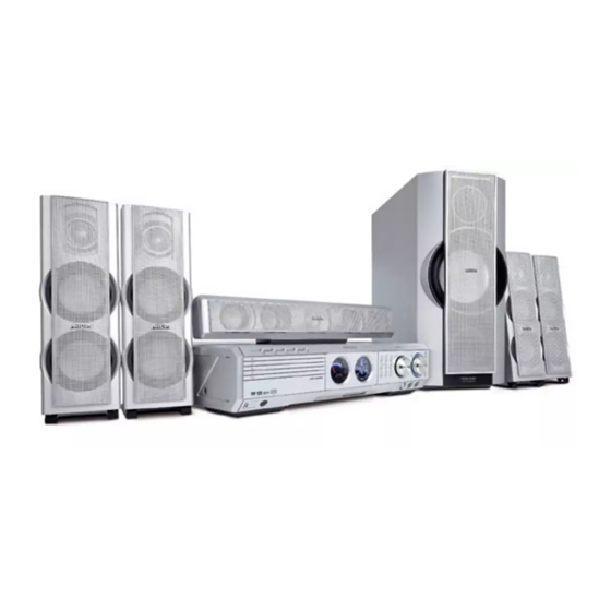
DVD Receiver
Service
Service
Service
Service
Service
Service Manual
©
Copyright 2003 Philips Consumer Electronics B.V. Eindhoven, The Netherlands
All rights reserved. No part of this publication may be reproduced, stored in a retrieval system or
transmitted, in any form or by any means, electronic, mechanical, photocopying, or otherwise
without the prior permission of Philips.
Published by KC 0329 Service Audio
Version 1.1
TABLE OF CONTENTS
Location of pc boards & Version variations ................ 1-2
Technical Specifications ............................................. 1-3
Measurement setup .................................................... 1-4
Service Aids, Safety Instruction, etc. ......................... 1-5
Disassembly Instructions & Service positions ........... 2-1
Service Test Programs ............................................... 3-1
Region codes setting, software upgrades, etc ........... 3-3
Set Block diagram & Wiring diagram ............................ 4
PCMCIA board ............................................................... 5
Front Board .................................................................... 6
ECO6 Tuner Board:
System Non-Cenelec ............ 7A
System Cenelec .................... 7B
Power Module PWR207 ................................................ 8
AV Board ........................................................................ 9
5DTC Module ............................................................... 10
CD222 FE (Front End) Board ...................................... 11
CD222 BE (Back End) Board ...................................... 12
Set Mechanical Exploded view & parts list ................. 13
History .......................................................................... 14
Printed in The Netherlands
Subject to modification
MX5500D/
21S/37
MX5700D/
Page
& MX5600D/
37
21R/21S/22S/25S
CLASS 1
LASER PRODUCT
GB
3139 785 30211
Advertisement
Chapters
Table of Contents

Related Manuals for Philips MX5500D/21S


Summary of Contents for Philips MX5500D/21S
- Page 1 LASER PRODUCT © Copyright 2003 Philips Consumer Electronics B.V. Eindhoven, The Netherlands All rights reserved. No part of this publication may be reproduced, stored in a retrieval system or transmitted, in any form or by any means, electronic, mechanical, photocopying, or otherwise without the prior permission of Philips.
-
Page 2: Location Of Pc Boards
LOCATION OF PC BOARDS AMPLIFER BOARD SPK II BOARD ECO6 TUNER MAINS & ECO SPK I BOARD 100W = 2PCS BOARD STBY BOARD 75W = 1PC AV BOARD 5DTC-DVD LOADER MECHANISM CONTROL CD222 FE BOARD BOARD CD222 BE BOARD SUPPLY BOARD FRONT FRONT... - Page 3 SPECIFICATIONS AMPLIFIER: GENERAL: Output power for 75W versions (MX5500D/21S/33S) Mains voltage : 110-127V/220-240V Switchable for /21.. Stereo mode (DIN) : 2 x 75W RMS 120V for /37 Surround mode : 75W RMS/channel 240V for /25S Output power for 100W versions (other versions)
-
Page 4: Measurement Setup
MEASUREMENT SETUP Tuner FM Bandpass LF Voltmeter 250Hz-15kHz e.g. PM2534 e.g. 7122 707 48001 RF Generator e.g. PM5326 S/N and distortion meter e.g. Sound Technology ST1700B Use a bandpass filter to eliminate hum (50Hz, 100Hz) and disturbance from the pilottone (19kHz, 38kHz). Tuner AM (MW,LW) Bandpass LF Voltmeter... - Page 5 SERVICE AIDS Service Tools: ESD Equipment: Universal Torx driver holder ........4822 395 91019 Anti-static table mat - large 1200x650x1.25mm ... 4822 466 10953 Torx bit T10 150mm ..........4822 395 50456 Anti-static table mat - small 600x650x1.25mm ..4822 466 10958 Torx driver set T6 - T20 .........
- Page 6 WAARSCHUWING WARNING Alle IC’s en vele andere halfgeleiders zijn All ICs and many other semi-conductors are gevoelig voor electrostatische ontladingen susceptible to electrostatic discharges (ESD). (ESD). Careless handling during repair can reduce life Onzorgvuldig behandelen tijdens reparatie kan drastically. de levensduur drastisch doen verminderen. When repairing, make sure that you are Zorg ervoor dat u tijdens reparatie via een connected with the same potential as the mass...
-
Page 7: Dismantling Instructions
DISMANTLING INSTRUCTIONS Dismantling of the Front Panel assembly Dismantling the Tuner, Mains and AV boards 2) Loosen 5 screws A and 8 catches C1 to slide the Front 1) Loosen 3 screws D and 2 catches C2 on the Rear panel 4) Loosen 7 screws F (8 screws for Scart version) and 2 C5 1) Loosen the 9 screws to dismantle the Top Cover (pos (pos 251) to remove the Tuner board assemby (pos 1101) - Page 8 Service positions Dismantling the Mono FE and BE boards Service position A (Top cover removed) 1) Loosen 2 screws and 2 catches to remove the Mono BE board (pos 1103-B). 2) Loosen 2 screws and 2 catches to remove the Mono FE board (pos 1103-C).
- Page 9 Service positions Service position C (Supply and Amplifier boards loosen) Service position D (Mains & AV boards loosen) Amplifier Board (Top piece) Mains Board Amplifier Board with non- (Bottom piece) conductive insulation attached to the copper pattern Thick paper Supply Board Thick paper Caution: Service position E (5DTC Mechanism, Mono FE and Mono...
- Page 10 SERVICE TEST PROGRAM I To start service test program hold DISC1 & STANDBY-ON buttons depressed while plugging in the mains cord* * Hold till the Display is shown S refers to Service Mode Display shows the V refers to Version ROM version yy refers to Software version number of the uProcessor "S-Vyy"...
- Page 11 SERVICE TEST PROGRAM II To start service test program hold DISC1 & STANDBY-ON buttons depressed while plugging in the mains cord* * Hold till the Display is shown S refers to Service Mode Display shows the ROM version V refers to Version "S-Vyy"...
- Page 12 1) Press <DISC MENU> followed by numerical keys <1> <5> <9> The set display shows: “- 0 - 0 - 0 - 0 - ” 2) Press now successively the following numerical keys : for MX5500D/21S <3><2><4> <0><1><1> <0><0> for MX5500D/33S <3><5><4>...
- Page 13 SET BLOCK DIAGRAM Power Amplifier ECO 6 TDA8920 DVD Module POWER AMP TDA8920 SURROUND POWER AMP 1/2XTDA8920 1/2XTDA8920 Mains and Regulator MAINS TRAFO LPS COIL ECO Standby Front Display TMP88CU74F Note: All others are in the AV board. MX3900D_130_wk302-2...
-
Page 14: Power Module
MAIN WIRING DIAGRAM 120mm 240mm 180mm TUNER 140mm for ECO SET ONLY for ECO SET ONLY 180mm POWER MODULE Refer to page 4-3 for details 400mm Prefold 180mm Prefold FRONT DISPLAY 180mm MX55/56/58/59 Prefold MX3900D 400mm Prefold DVD Module DVD_SC SCART 0 GND_Sc Mute_AV... - Page 15 WIRING DIAGRAM - POWER MODULE DETAILS 120mm 240mm SUPPLY TRAFO NOTE : 180mm 75W 6-CHANNEL : 1 X CLASS-D AMPLIFIER + SPK I VH 3X 75W 7-CHANNEL : 1 X CLASS-D AMPLIFIER + SPK I + SPK II 150mm 100W : 2 X CLASS-D AMPLIFIER + SPK I + SPK II Blue/Yellow Red/Black VH 3X...
- Page 16 WIRING DIAGRAM - DVD MODULE DETAILS TO 5DTC MECH ASSY TO AV BOARD CON1405 TO 5DTC MECH ASSY CD222 BE CD222 FE Optical FMN 1501 +3V3_SENSE Lightpen +3V3 +3V3 GND_D PH 1106 GND_D TO AV BOARD GND_D GND_D GND_D GND_D CON1242 HDASP HDASP...
- Page 17 Notes: PCMCIA BOARD TABLE OF CONTENTS Circuit Diagram ................5-2 Component & Chips Layout ............5-3 Electrical parts list ................5-4...
- Page 18 CIRCUIT DIAGRAM 1500 A7 2510 E2 2513 F6 3500 C3 3503 B3 3506 A3 3509 A3 3512 B3 3515 C3 3522 C3 3525 D3 3528 D3 3531 E3 3545 B9 3550 F9 3553 F8 3556 E7 3559 E5 3562 E4 3570 A3 4520 B6 4570 E1...
- Page 19 COMPONENT & CHIPS LAYOUT This assemby drawing shows a summary of all possible versions. For components used in a specific version see This assemby drawing shows a summary of all possible versions. For components used in a specific version see schematic and respective parts list.
- Page 20 ELECTRICAL PARTS LIST - PCMCIA BOARD MISCELLANEOUS 3139 118 56571 PCMCIA Board Assembly 3563 4822 117 13632 100k 1% 0,62W 1500 2422 025 18005 Socket PCMCIA 68P 3564 4822 117 13632 100k 1% 0,62W 4501 4822 051 30008 0R Jumper 0603 1542 2422 025 17371 Flex Socket 40P...
-
Page 21: Table Of Contents
FTD DISPLAY PIN CONFIGURATION BLOCK DIAGRAM /CS1 /RES LCD DISPLAY 48 X 15 DOTS + ICONS LCD CONTROLLER/ D0 - D7 DRIVER 'SITRONIX' ST7522 FRONT BOARDS (Die form) WHITE LED BACKLIGHT LED+ LED- TABLE OF CONTENTS FTD Display Module pin configuration ............6-1 Front Display part - Circuit diagram ............. -
Page 22: Front Display Part - Circuit Diagram
& QUALITY 9 MODE TU_GND CTRL +5V6 @3131 values GND_B 3111 1N4003 TuRdsData not use MX5500D/37 3130 VSSA VSSD MX5500D/21S/33S/35S 13 14 680K MX5700D/22S/25S 3113 3114 MX5600D/37, MX5700D/21R/21S 7105 220K +5V6 +5V6 BC847B 5105 2106 2107 AT-51 8239 210 9500 pt3/4 dd wk0329... - Page 23 FRONT DISPLAY PART - COMPONENT & CHIPS LAYOUT This assemby drawing shows a summary of all possible versions. For components used in a specific version see schematic and respective parts list. 8239 210 9500 pt3 dd wk0317 This assemby drawing shows a summary of all possible versions. For components used in a specific version see schematic and respective parts list. PART B PART A 8239 210 9500 pt3 dd wk0317...
-
Page 24: Front Display Part - Chip Layout Part A
FRONT DISPLAY PART - CHIPS LAYOUT PART A This assemby drawing shows a summary of all possible versions. For components used in a specific versio PART A... -
Page 25: Front Display Part - Chip Layout Part B
FRONT DISPLAY PART - CHIPS LAYOUT PART B specific version see schematic and respective parts list. PART B 8239 210 9500 pt3 dd wk0317... -
Page 26: Front Control Part - Chip Layout
FRONT CONTROL PART - CHIPS LAYOUT This assemby drawing shows a summary of all possible versions. For components used in a specific version see schematic and respective parts list. 8239 210 9412 pt3 dd wk0317... -
Page 27: Front Control Part - Component Layout
FRONT CONTROL PART - COMPONENT LAYOUT This assemby drawing shows a summary of all possible versions. For components used in a specific version see schematic and respective parts list. 8239 210 9412 pt3 dd wk0317... -
Page 28: Front Control Part - Circuit Diagram
FRONT CONTROL PART - CIRCUIT DIAGRAM 1300 A1 1304 A5 1308 A6 1313 C1 2304 B5 2308 D3 3304 A4 3308 A5 3312 A7 3333 A1 3337 D5 3341 D5 3345 C6 3349 E6 6300 C6 6304 E6 7300 C5 7304 C8 7308 E8 1301 A3... -
Page 29: Dtc Key Part - Component & Chip Layouts
DTC KEY PART - COMPONENT & CHIP LAYOUTS This assemby drawing shows a summary of all possible versions. For components used in a specific version see schematic and respective parts list. 8239 210 9413 pt3 dd wk0317 This assemby drawing shows a summary of all possible versions. For components used in a specific version see schematic and respective parts list. 8239 210 9413 pt3 dd wk0317... -
Page 30: Dtc Key Part - Circuit Diagram
6-10 6-10 DTC KEY PART - CIRCUIT DIAGRAM POWER SWITCH PART - CIRCUIT DIAGRAM 1400 A1 1402 A2 1404 A3 2400 A3 3401 A2 3403 A3 1500 B1 2501 B2 3501 C3 3503 B2 3505 A2 6500 C3 7500 C3 7504 A2 1401 A2 1403 A2... - Page 31 6-11 6-11 POWER SWITCH PART - COMPONENT & CHIPS LAYOUT This assemby drawing shows a summary of all possible versions. For components used in a specific version see schematic and respective parts list. This assemby drawing shows a summary of all possible versions. For components used in a specific version see schematic and respective parts list.
-
Page 32: Hdph & Mic Part - Circuit Diagram (Non-Karaoke Version)
6-12 6-12 HDPH & MIC PART - CIRCUIT DIAGRAM (For non-Karaoke version pt 3 pcb only) 1600 A3 1602 A6 1604 B5 2600 A4 2602 A5 2604 B4 2606 C3 2608 C4 2610 C4 3605 C4 3607 B5 3609 B5 3611 C5 3613 C2 3615 C5... - Page 33 6-13 6-13 HDPH & MIC PART - COMPONENT & CHIP LAYOUTS (For non- Karaoke version pt 3 pcb only)
-
Page 34: Hdph & Mic Part - Circuit Diagram (Karaoke Version)
6-14 6-14 HDPH & MIC PART - CIRCUIT DIAGRAM (For all versions pt 4 pcb) 1600 A3 1602 A6 1604 B5 2600 B5 2602 B5 2604 C4 2606 C3 2608 C4 2610 C4 3605 C4 3607 B5 3609 C5 3611 C5 3613 C2 3615 C5 5603 B5... - Page 35 6-15 6-15 HDPH & MIC PART - COMPONENT & CHIP LAYOUTS (For all versions pt 4 pcb)
- Page 36 6-16 6-16 ELECTRICAL PARTS LIST - FRONT BOARDS ELECTRICAL PARTS LIST - FRONT BOARDS MISCELLANEOUS 3139 119 00831 LCD Module MX5500D-01 2119 2238 586 59812 100nF +80/-20% 50V 3117 4822 051 30102 1k 5% 0,062W 3339 4822 051 30121 120R 5% 0,062W 2120 2238 586 59812 100nF +80/-20% 50V...
- Page 37 6-17 6-17 ELECTRICAL PARTS LIST - FRONT BOARDS ELECTRICAL PARTS LIST - FRONT BOARDS RESISTORS 4137 4822 051 30008 0R Jumper 0603 4192 4822 051 30008 0R Jumper 0603 4245 4822 051 30008 0R Jumper 0603 4602 4822 051 30008 0R Jumper 0603 4138 4822 051 30008...
-
Page 38: Electrical Partslist
7A-1 7A-1 BLOCK DIAGRAM TUNER BOARD ECO 6 Systems Vcc1 buffer ampl. Stab Stab Discriminator FM-RF FM-IF 1 FM-IF 2 (MPX) Vcc2 1101 Loop (1102) LF filter 10,7 MHz 10,7 MHz 10,7 MHz 1120 left left Stereo right right Det. Decoder Frontend Mixer... - Page 39 7A-2 7A-2 1101 A1 1102 B1 1103 F2 1120 E14 1130 A2 TUNER BOARD ECO6 1131 B2 / SYSTEMS NON CENELEC 1132 G13 2101 B3 VERSION PROGRAMMING COMPONENTS 2102 B1 1101 2103 C7 2105 2104 B3 AM-IF1 1130 2105 A2 100n 5111 450kHz...
- Page 40 7A-3 7A-3 1101 A6 1120 A4 1132 A5 2128 C4 2138 C2 3142 D2 5110 B3 5114 A2 5123 D5 7112 C1 9104 B5 9107 D4 TUNER ADJUSTMENT TABLE ( ECO6 FM/MW- and FM/MW/LW - versions with AM-frame aerial ) 1102 B6 1130 B5 2106 C5...
- Page 41 7A-4 7A-4 Electrical Partslist ECO6 SYSTEMS NON CENELEC MISCELLANEOUS RESISTORS ––––––––––––––––––––––––––––––––––––––––––––––––––––– ––––––––––––––––––––––––––––––––––––––––––––––––––––– 1101 2422 015 19376 SOCKET 2P CLICKFIT 3143 © 4822 051 20223 22kΩ 0,1W USA only RDS only 1102 4822 267 10283 SOCKET COAX, IEC 75Ω 3144 © 4822 051 10102 1kΩ...
- Page 42 7B-1 7B-1 BLOCK DIAGRAM ECO6 Tuner Board SYSTEMS CENELEC version: TABLE OF CONTENTS Blockdiagram ..............7B-1 Schematic Diagram ............7B-2 Component Layout............7B-3 Adjustment table .............7B-3 Electrical Partslist ............7B-4...
- Page 43 7B-2 7B-2 1101 A2 5121 E11 1102 B1 5122 H5 1103 E2 5123 G5 1110 B2 6105-1 E4 VERSION PROGRAMMING COMPONENTS 1120 E14 6105-2 G6 TUNER BOARD ECO6 1130 A2 6106 D4 / SYSTEMS-CENELEC 1131 C2 6107 G13 VERSION AM-IF1 1132 F13 6120 C13 6120...
- Page 44 7B-3 7B-3 1101 B5 1110 B4 1131 C5 2107 B3 2133 C1 2162 A4 5102 C4 5110 A2 5114 A2 5121 B2 7104 C4 9101 A2 9104 B1 9107 B4 9110 A4 TUNER ADJUSTMENT TABLE ( ECO6 Cenelec FM/MW - and FM/MW/LW - versions with AM-frame aerial ) 1102 B5 1120 A4 1132 A4...
- Page 45 7B-4 7B-4 Electrical Partslist ECO6 SYSTEMS CENELEC MISCELLANEOUS RESISTORS DIODES ––––––––––––––––––––––––––––––––––––––––––––––––––––– ––––––––––––––––––––––––––––––––––––––––––––––––––––– ––––––––––––––––––––––––––––––––––––––––––––––––––––– 1101 2422 015 19376 SOCKET CLICKFIT 2P 3128 © 4822 117 11449 2,2kΩ 0,1W 6105 © 4822 130 83075 HN1V02H USA only LW only 1102 4822 267 10283 SOCKET COAX, IEC 75Ω...
- Page 46 6-channel class-D amplifier Basic operation of a class-D amplifier Basically, the output stage of a class-D amplifier outputs a continuous square wave swinging between positive and negative power supplies with a fixed frequency (“clock” frequency) far beyond the audible range. The duty cycle of this square wave is modulated with the audio signal. The output is followed by a low-pass filter which eliminates the clock frequency and allows only the audio signal going to the speaker.
-
Page 47: Mechanical Exploded View
MECHANICAL EXPLODED VIEW Block diagram and operation SINGLE ENDED 6 x 75W BRIDGE 3 x 100W TDA8920 TDA8920 output 1 input 1 output 1 input 1 input 2 output 2 TDA8920 TDA8920 output 2 input 3 output 3 input 2 input 4 output 4 TDA8920... - Page 48 SW-OUT (SPK II) BOARD - CIRCUIT & LAYOUT DIAGRAMS (For Twin Subwoofer versions only) 1305-A A3 1305-B B3 1305-F B5 1322 B1 2018 A2 2019 A4 2020 B4 1305-A 2021 B4 LQR0410 2022 C4 3006 A2 2018 3006 220n EH-B 1322 1305-B LQR0410...
-
Page 49: Speaker (Spk I) Board - Circuit Diagram
SPEAKER (SPK I) BOARD - CIRCUIT DIAGRAM 1303-A E4 1303-F B4 1304-E B3 1317 B2 2000 A4 2005 C4 2010 E4 2015 C2 3002 C3 1303-B B4 1304-A B3 1313 A1 1318 E2 2001 A4 2006 C4 2011 E4 2016 D3 3003 C3 1303-C A4 1304-B A3... -
Page 50: Speaker (Spk I) Board - Componet & Chip Layouts
SPEAKER (SPK I) BOARD - COMPONENT & CHIP LAYOUTS This assemby drawing shows a summary of all possible versions. For components used This assemby drawing shows a summary of all possible versions. For components used in a specific version see schematic and respective parts list. in a specific version see schematic and respective parts list. -
Page 51: Mains & Eco Stby Board - Circuit Diagram
MAINS & ECO STBY BOARD - CIRCUIT DIAGRAM 1901 A1 1908 B10 1912 B5 2904 D9 2908 E3 2912 E10 3901 C2 3905 D10 3909 E6 3914 E2 3918 D2 5901 A1 5905 D9 6904 D10 6908 D8 6912 E5 6917 E6 6921 C10 7905 E7... -
Page 52: Mains & Eco Stby Board - Component & Chip Layouts
MAINS & ECO STBY BOARD - COMPONENT & CHIP LAYOUTS This assemby drawing shows a summary of all possible versions. For components used in a specific version see schematic and respective parts list. This assemby drawing shows a summary of all possible versions. For components used in a specific version PART A see schematic and respective parts list. -
Page 53: Mains & Eco Stby Board - Chip Layouts Part A
MAINS & ECO STBY BOARD - CHIP LAYOUT PART A This assemby drawing shows a summary of all possible versions. For components used in a specific version see schematic and respective parts list. PART A... -
Page 54: Mains & Eco Stby Board - Chip Layouts Part B
MAINS & ECO STBY BOARD - CHIP LAYOUT PART B PART B 8239 210 93434 .. 3139 113 3494pt4 dd wk0315... -
Page 55: Supply Board - Circuit Diagram
8-10 8-10 SUPPLY BOARD - CIRCUIT DIAGRAM 1100 D6 1205 D2 1264 B10 2202 E8 2206 A8 2211 D4 2217 E3 2222 A4 2226 B6 3201 A6 3205 A7 3209 B5 3217 E7 3223 E8 3227 D7 3231 C3 6203 C4 6211 A3 6216 C3 7202 A7... - Page 56 8-11 8-11 SUPPLY BOARD - COMPONENT LAYOUT SUPPLY BOARD - CHIP LAYOUT This assemby drawing shows a summary of all possible versions. For components used in a specific version This assemby drawing shows a summary of all possible versions. For components used in a specific version see schematic and respective parts list.
-
Page 57: Supply Board - Chip Layout Part A
8-12 8-12 SUPPLY BOARD - CHIP LAYOUT PART A This assemby drawing shows a summary of all possible versions. For components used in a specific version see schematic and respective parts list. PART A... -
Page 58: Supply Board - Chip Layout Part B
8-13 8-13 SUPPLY BOARD - CHIP LAYOUT PART B PART B 8239 210 93414 .. 3139 113 3494pt4 dd wk0315... - Page 59 8-14 8-14 AMPLIFIER BOARD - CLOCK GENERATOR & CONNECTION CIRCUIT 1301 B1 6505 B10 1302 B2 6506 C10 1303 E2 6507 C10 1304 G2 6508 C10 1305 E1 6600 F6 1309 G1 6713 H12 1312 G3 6714 H12 1320 I6 6715 I12 1400 I6 7500 A12...
-
Page 60: Amplifier Board - Amplifier Circuit
8-15 8-15 AMPLIFIER BOARD - AMPLIFIER CIRCUIT 1306 A7 5303 I5 1307 H7 7100 A2 1308 E7 7200 D2 1316 B7 7300 H2 2106 1317 I7 F104 A7 1318 E7 F109 B7 2101 A3 F112 B7 2104 2107 2102 A3 F120 E7 100n 100n... -
Page 61: Amplifier Board - Bottom View
8-16 8-16 AMPLIFIER BOARD - BOTTOM VIEW This assembly drawing shows a summary of all possible versions. For components used in a specific version see schematics and respective parts list. PART A 3104 213 3525 bl132-2 dd 19-11-02 PART B... -
Page 62: Amplifier Board - Top View
8-17 8-17 AMPLIFIER BOARD - TOP VIEW This assembly drawing shows a summary of all possible versions. For components used in a specific version see schematics and respective parts list. PART C 3104 213 35254 bl132-1 dd 19-11-02 PART D... -
Page 63: Amplifier Board - Bottom View Part A
8-18 8-18 AMPLIFIER BOARD - BOTTOM VIEW PART A This assembly drawing shows a summary of all possible versions. For components used in a specific version see schematics and respective parts list. PART A... -
Page 64: Amplifier Board - Bottom View Part B
8-19 8-19 AMPLIFIER BOARD - BOTTOM VIEW PART B 3104 213 3525 bl132-2 dd 19-11-02 PART B... -
Page 65: Amplifier Board - Top View Part C
8-20 8-20 AMPLIFIER BOARD - TOP VIEW PART C This assembly drawing shows a summary of all possible versions. For components used in a specific version see schematics and respective parts list. PART C... -
Page 66: Amplifier Board - Top View Part D
8-21 8-21 AMPLIFIER BOARD - TOP VIEW PART D 3104 213 35254 bl132-1 dd 19-11-02 PART D... - Page 67 47nF 16V 3918 4822 116 52175 100R 5% 0,5W 7205 4822 130 60373 BC857B 1905 4822 071 53152 Fuse T3.15A 250V MX5500D/21S 2904 2238 586 59812 100nF +80/-20% 50V 3919 4822 051 30152 1k5 5% 0,062W 7206 4822 130 60373 BC857B...
- Page 68 8-23 8-23 ELECTRICAL PARTS LIST - AMPLIFIER BOARD ELECTRICAL PARTS LIST - AMPLIFIER BOARD MISCELLANEOUS 2228 2222 580 15649 100nF 10% 50V 2420 5322 126 11578 1nF 10% 50V 3406 4822 051 30562 5k6 5% 0,063W not for 75W 3104 211 29861 Spring, IC 2229 2222 580 15649...
-
Page 69: Electrical Parts List - Amplifier Board
8-24 8-24 ELECTRICAL PARTS LIST - AMPLIFIER BOARD RESISTORS 4338 4822 051 20008 0R JUMPER 0805 4400 4822 051 30008 0R JUMPER 0603 not for 75W COILS & FILTERS 5102 2422 536 00496 IND. FXD. 22uH 10% 5103 2422 536 00496 IND. - Page 70 BRIEF INTRODUCTION OF THE AV BOARD The AV Board consists of the following features : IC 7130 (TDA7468D) IC 7130 provides the source selection (TUNER, TV/AV Digital in, DVD/CD & AUX) and basic sound processing - bass, treble, volume & mute controls for the Front L/R loudspeakers. Note: Although provided for, the AUX source (pin 3 and 26) are never selected &...
- Page 71 INPUT, SOURCE SELECT & VOLUME CONTROL L/R CIRCUIT 1100 C8 3154 H5 1152 B1 3155 H5 1181-1 G2 3156 I4 1181-2 G2 3157 I5 FOR PRODUCTION USE ONLY 1181-5 H1 3158 I3 3160 1182-A I2 3159 I4 1182-B F2 3160 A9 7422 : TRUTH_TABLE 1237 B2 3161 D7...
- Page 72 PRE-AMPLIFIER, SUPPLY & INTERCONNECTION CIRCUIT 1200 E9 1233 E9 1240 D12 1245 D13 2208 F3 2213 C1 2218 G1 2226 G5 2231 H9 2242 E6 2283 D8 3204 B7 3209 A5 3214 B4 3231 D2 3236 E1 3243 H2 3254 G7 3261 G6 3269 G7 3274 E5...
- Page 73 VOLUME CONTROL SURR., CENTER & SW AND CONTROL MULTIPLEXER CIRCUIT 1234 E11 2303 C8 2308 D7 2311 B3 2314 C3 2320 C1 2324 F9 2327 G7 2330 G7 2333 H6 2336 F3 2339 G3 2342 G1 2349 A13 2380 G8 3302 G8 3305 B7 3308 D8...
-
Page 74: C Expander Circuit
DIGITAL I/O, S-VIDEO, SCART, & I C EXPANDER CIRCUITS 1181-3 G1 1401 A1 2403 D12 2412 F13 2421 I6 2428 G3 2435 A9 3405 B11 3418 I10 3426 F12 3434 E8 3444 G2 3451 C3 3459 E4 3466 B8 4116 H13 4406 E8 4413 B13 4421 C6... - Page 75 BOTTOM VIEW - SMD & COMPONENT This assembly drawing shows a summary of all possible versions. For components used in a specific version see schematic diagram and respective parts list PART A PART B The following reworks are make at prod. start-up on the SMD side: 1.
- Page 76 TOP VIEW - CHIP & COMPONENT This assembly drawing shows a summary of all possible versions. For components used in a specific version see schematic diagram and respective parts list PART E PART F PART G PART H 3139 113 3500 pt5 dd wk318...
-
Page 77: Bottom View Part A
BOTTOM VIEW - PART A PART A... -
Page 78: Bottom View Part B
BOTTOM VIEW - PART B PART B... -
Page 79: Bottom View Part C
9-10 9-10 BOTTOM VIEW - PART C PART C 2 chip cap 4,7nF... -
Page 80: Bottom View Part D
9-11 9-11 BOTTOM VIEW - PART D PART D... - Page 81 9-12 9-12 BOTTOM VIEW - PART E PART E...
- Page 82 9-13 9-13 BOTTOM VIEW - PART F PART F...
- Page 83 9-14 9-14 BOTTOM VIEW - PART G PART G...
- Page 84 9-15 9-15 BOTTOM VIEW - PART H PART H...
- Page 85 9-16 9-16 ELECTRICAL PARTS LIST - AV BOARD ELECTRICAL PARTS LIST - AV BOARD MISCELLANEOUS 1181 2422 026 05399 Socket Aux-in/Digital-In/Out 2139 2238 586 59812 100nF +80/-20% 50V 2254 3198 017 44740 470nF 10V 2403 3198 017 42230 22nF 50V Scart 1182 4822 265 11151...
- Page 86 9-17 9-17 ELECTRICAL PARTS LIST - AV BOARD ELECTRICAL PARTS LIST - AV BOARD RESISTORS 3125 4822 051 30271 270R 5% 0,062W 3210 4822 051 30102 1k 5% 0,062W 3313 4822 051 30102 1k 5% 0,062W 3425 4822 051 30689 68R 5% 0,063W 3126 4822 051 30271...
- Page 87 9-18 9-18 ELECTRICAL PARTS LIST - AV BOARD ELECTRICAL PARTS LIST - AV BOARD RESISTORS 4192 4822 051 30008 0R Jumper 0603 4520 4822 051 30008 0R Jumper 0603 5401 4822 157 10586 2,2uH 10% 7451 4822 130 42804 BC817-25 4195 4822 051 30008 0R Jumper 0603...
- Page 88 10-1 5DTC MODULE (DVD Version) TABLE OF CONTENTS Emergency opening ..............10-2 Location of switches ..............10-3 Blockdiagram ................10-3 Control Board Circuit diagram ................10-4 Component Layout ............... 10-4 Exploded view loader ..............10-5 Mechanical assembly drawing + mechanical parts list ....10-6 Electrical parts list ................
-
Page 89: Emergency Opening
10-2 Emergency opening of the trays The trays of the 5DTC are mechanically Release snap as shown in picture 5 and pull tray out. locked. To open tray 1, 2 and 3 move lever (pos 29) backwards To remove a CD from Play Position perform following (e.g. -
Page 90: Location Of Switches
10-3 10-3 Blockdiagram MOTOR BOARD CONTROL BOARD SWITCH SWITCH 7801 HOLDER HEIGHT COLLECTOR DISC SENSOR COLLECTOR HOME SW HOME SW HOME SW OPEN SW HOLDER HEIGHT COLLECTOR OPEN SW UNLOAD SW OPEN SW Pin 1..3 not used! ADDRESS1 SW 1802 LOAD SW UNLOAD SW TRAY_IRQ... - Page 91 10-4 10-4 APPING FOR IRCUIT IAGRAM 5DTC CONTROL BOARD Mapping 1800 2810 3804 3811 3824 3833 3841 3854 3862 7805-B D3 1801 2811 3805 3815 3826 3834 3842 3855 3863 7806 1800 3832 1802 1801 3833 1802 2812 3806 3816 3827 3835 3843...
- Page 92 10-5 10-5 Exploded view 5DTC mechanic - for orientation only...
- Page 93 10-6 10-6 DVD MODULE COMPONENTS ELECTRICAL PARTS LIST - CONTROL BOARD MISCELLANEOUS 1800 4822 242 72066 Ceram Filter 8MHz 3841 4822 051 30103 10k 5% 0,062W 1601 3842 4822 051 30103 10k 5% 0,062W 1801 2422 025 17065 FFC Connector 16Pin Vert. 3845 4822 051 20159 15R 5% 0,1W...
-
Page 94: Component Layout
11-1 11-1 M29F002BT V CC A0-A17 DQ0-DQ7 M29F002BT M29F002BT MONO-FE BOARD V SS Function Description A0-A17 Address Inputs DQ0-DQ7 Data Inputs/Outputs Chip Enable Output Enable Write Enable M29F002BT, M29F002BB: Reset/Block Temporary Unprotect M29F002BNT, M29F002BNB: TABLE OF CONTENTS Not Connected Internally Supply Voltage M29F002BT .................. - Page 95 11-2 11-2 M5705 (Ali) Features M5705 (Ali) Application Data Separator Target Search 4M DRAM Built-in data slicer and data PLL for data Built-in target sector searching circuit recovery from RF signal. for auto-searching the target sector. M5703/M5707 M5705 Supports digital/analog slice level Automatic data buffering after the adjustment.
- Page 96 11-3 11-3 M5705 Pins Descriptions Pin Name Pin No. Type Description Pin Name Pin No. Type Description Servo Data Slicer Interface Pins Microcontroller Interface Pins XSRFIN I / A Analog RF signal input after passing through the equalizer. XGPIO[2:0] 48,51,5 1.
- Page 97 11-4 11-4 M5705 Pins Descriptions Pin Name Pin No. Type Description Pin Name Pin No. Type Description Host Interface Pins RAM Interface Pins XHCS1J This pin is used to select the command block task file registers. XRSDCLK This signal is the clock output for SDRAM. XROEJ This signal is used as the memory output enable for external DRAM buffers.
- Page 98 11-5 11-5 M5705 Pins Descriptions SP32721A Internal Block Diagram Pin Name Pin No. Description AGC HOLD FAST Attackoff Power Pins PROGRAMMABLE DVDRFP EQUALIZER IMPUT AVDD5_DS Analog Power +5V for Data Slicer part. FULL WAVE FILTER BIAS DVDRFN DIFFERENTIATOR RECTIFIER CHARGE OUTPUT INHIBIT AVDD5_DA Analog Power +5V for DAC part.
- Page 99 11-6 11-6 TOP VIEW - SMD & COMPONENT LAYOUT 1101 O9 2310 J3 3301 H6 1102 C9 2311 I3 3302 C10 1103 B8 2312 J7 3303 C9 1104 F2 2313 C3 3304 C3 1105 I13 2314 B6 3305 E3 1106 M13 2315 D7 3306 F3 1107 M2...
- Page 100 11-7 11-7 BOTTOM VIEW - COMPONENT LAYOUT 1105 I13 1106 M13 1200 B11 2201 J8 2202 H9 2203 M6 2204 O6 2205 O6 2206 M11 2207 L11 2208 E9 2209 D9 2210 N3 2211 N5 2212 L5 2213 O4 2214 M4 2215 I3 2216 K3 2217 J11...
- Page 101 11-8 11-8 SERVO AMPLIFIERS & MOTOR DRIVERS CIRCUIT 1101 F2 2029 C10 2035 D11 2041 E7 2048 G11 2054 G7 2070 B2 2077 H1 2207 H10 2307 A4 3031 D9 3038 F7 3050 E14 3068 G8 3091 B1 3097 B2 3104 B5 3110 B7 4041 I8...
- Page 102 11-9 11-9 CD/DVD ROM CONTROLLER CIRCUIT 1104 D14 3304-1 G11 1200 I2 3304-2 G11 2001 B5 3304-3 G11 2002 I12 3304-4 G11 +3V3R 2003 B5 3305-1 G11 2004 H13 3305-2 H11 2301 100n 3118 5011 2302 100n 2005 B5 3305-3 G11 +3V3 3305-4 H11 2006 B4...
- Page 103 11-10 11-10 ELECTRICAL PARTS LIST - MONO-FE BOARD ELECTRICAL PARTS LIST - MONO-FE BOARD MISCELLANEOUS 3139 118 56941 FE (Front End) PCB Assembly CD222 2052 2222 867 15339 33pF 5% 50V 2307 2238 586 59812 100nF 50V 3060 4822 051 30339 33R 5% 0,062W 1101 2422 025 17529...
- Page 104 11-11 ELECTRICAL PARTS LIST - MONO-FE BOARD RESISTORS 7207 4822 130 42804 BC817-25 3311 4822 117 13578 RES NETWORK 4 X 10k 5% 1206 3312 4822 117 13578 RES NETWORK 4 X 10k 5% 1206 7208 9322 163 24668 L78M08CDT 3313 3198 031 11010 RST NETWORK 4 X 100R 5% 1206...
- Page 105 12-1 12-1 CS8415A MONO-BE BOARD M29F800DT Logic Diagram TABLE OF CONTENTS CS8415A & M29F800DT Internal Block Diagram ....... 12-1 Bottom View - Component Layout ..........12-2 Top View - SMDs & Component Layout ........12-3 Top View - SMDs & Component Layout Part A ......12-4 Top View - SMDs &...
-
Page 106: Bottom View - Component Layout
12-2 12-2 BOTTOM VIEW - COMPONENT LAYOUT... -
Page 107: Top View - Smds & Component Layout
12-3 12-3 TOP VIEW - SMD & COMPONENT LAYOUT PART A PART B... -
Page 108: Top View - Smds & Component Layout Part A
12-4 12-4 TOP VIEW - SMD & COMPONENT LAYOUT PART A PART A... -
Page 109: Top View - Smds & Component Layout Part B
12-5 12-5 TOP VIEW - SMD & COMPONENT LAYOUT PART B PART B... -
Page 110: Circuit Diagram 1
12-6 12-6 CIRCUIT DIAGRAM 1 1300 C14 1811 I1 2304 B4 2309 B8 2315 D9 2320 D11 2331 H10 2337 H11 2342 A4 2347 A6 2352 A7 2357 I8 2363 D12 3302 B9 3307 B10 3315 D9 3320 E8 3325 E8 3330 E9 3335 F8 3340 F9... -
Page 111: Circuit Diagram 2
12-7 12-7 CIRCUIT DIAGRAM 2 1401 G13 2404 D5 2409 H5 2414 I6 2419 B9 2426 C11 2431 D9 2438 F11 2443 G11 2454 H10 3403 E2 3408 F2 3413 G2 3418 D3 3423 B9 3428 B10 3433 D9 3438 E9 3443 F10 3448 G10 3453 I9... -
Page 112: Circuit Diagram 3
12-8 12-8 CIRCUIT DIAGRAM 3 1501 A2 1503 A3 1504 F3 1505 G3 2501 A10 2502 A10 SPDIF CONVERTER & ADC 2503 C7 2504 C7 2505 B5 2506 B5 2507 E10 2508 G8 1503 1501 2509 H8 +5VS 2510 F11 +3V3_SENSE +12V 2511 F11... - Page 113 12-9 12-9 ELECTRICAL PARTS LIST - MONO-BE BOARD ELECTRICAL PARTS LIST - MONO-BE BOARD MISCELLANEOUS 3139 118 56481 Mono BE Board Assy CD222 P 2346 2238 586 59812 100nF +80/-20% 50V 2440 2020 552 94427 100pF 5% 50V 3329 4822 051 30109 10R 5% 0,062W 2347 2238 586 59812...
- Page 114 12-10 12-10 ELECTRICAL PARTS LIST - MONO-BE BOARD RESISTORS 3424 4822 051 30123 12k 5% 0,062W 3521 4822 117 12139 22R 5% 0,062W 3584 4822 117 12139 22R 5% 0,062W 7402 4822 209 30095 LM833D 3425 4822 051 30153 15k 5% 0,062W 3522 4822 117 12139 22R 5% 0,062W...
- Page 115 13-1 13-1 EXPLODED VIEW - MAIN UNIT mx5500D Exploded view 3139 119 35120 dd wk315...
- Page 116 Cover Tray Disc2 9965 000 07586 Mains Cord 2A5 1,5M MX5600D /25S Breakdown of Satellite LS Package (For MX5500D/21S only) Breakdown of Subwoofer Box (For MX5500D family) 3139 118 19381 Cover Tray Disc3 2422 070 98246 Mains Cord UL 7A 1,5M...
- Page 117 13-3 EXPLODED VIEW - STAND SUBWOOFER (For MX5600D & MX5700D only) 2 PINS TERMINAL SHOTGUN TOP FOAM GASKET Screw size Mounting D3 x 10 2pcs 2-pins Terminal LOCKING TOP D3.5 x 15 3pcs Shotgun Top 2-SPRING D3 x 10 4pcs Locking Assy (Top &...
- Page 118 14-1 DOCUMENT HISTORY Version 1.0 Initial release Version 1.1 Add MX5700D/21R, MX5700D/21S and MX5700D/25S into existing service manual - Pages modified: Pg 1-1 to 1-3, 6-2, 6-16 to 6-17, 8-22, 9-16 to 9-18, 13-2...