Table of Contents
Advertisement
Quick Links
Download this manual
See also:
Instruction Manual
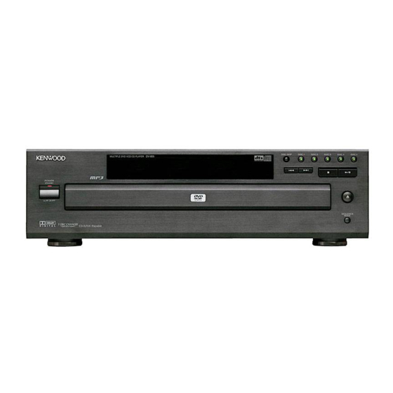
MULTIPLE DVD/VCD/CD PLAYER
DV-6050
SERVICE MANUAL
Cabinet panel
(A60-2323-08)
POWER
STANDBY
ON
OFF
Knob(POWER)
(K27-2503-08)
Top cover
(A01-3854-08)
Con DIN socket
(E63-1192-08)
In compliance with Federal Regulations, following are repro-
duction of labels on, or inside the product relating to laser
product safety.
Caution : No connection of ground line if disassemble
the unit. Please connect the ground line on
rear panel, PCBs, Chassis and some others.
Crystal Window
(B10-3936-08)
Con DIN socket
Con phono socket
(E68-0018-08)
(E63-1311-08)x2
Con phono socket
(E63-1244-08)
KENWOOD Corp. certifies this equipment conforms to DHHS
Regulations No.21 CFR 1040. 10, Chapter 1, subchapter J.
DANGER : Laser radiation when open and interlock defeated.
AVOID DIRECT EXPOSURE TO BEAM.
© 2002-10 PRINTED IN KOREA
B51-5831-00 (K/K) 1382
Button
(K29-8238-08)
DISC SKIP
4
Slide switch
Wire-MCRDM
(S62-0115-08)
(E30-7250-08)
DISC 2
DISC 3
DISC 4
DISC 5
DISC 1
¢
7
3
0
SEQUENCE MODE
Button
(K27-2502-08)
Clamp AC cord
(J42-0350-08)
70%
Advertisement
Table of Contents

Related Manuals for Kenwood DV-6050


Summary of Contents for Kenwood DV-6050
- Page 1 (S62-0115-08) (E30-7250-08) In compliance with Federal Regulations, following are repro- KENWOOD Corp. certifies this equipment conforms to DHHS duction of labels on, or inside the product relating to laser Regulations No.21 CFR 1040. 10, Chapter 1, subchapter J. product safety.
-
Page 2: Table Of Contents
DV-6050 CONTENTS / ACCESSORIES Contents CONTENTS / ACCESSORIES ........2 SCHEMATIC DIAGRAM .......... 28 DISASSEMBLY FOR REPAIR........3 EXPLODED VIEW ............43 CIRCUIT DESCRIPTION ..........4 PARTS LIST..............44 ADJUSTMENT ............19 SPECIFICATIONS ........Back cover INTERCONNECTION DIAGRAM ......20 PC BOARD .............. 21 Accessories Please confirm that the following accessories are present. -
Page 3: Disassembly For Repair
DV-6050 DISASSEMBLY FOR REPAIR 1. How to open the tray if it does not come out. 1. Remove the plastic plate. 2. Turn the gear fully CCW using a flat driver and so on in the drawing through the hole on the loading chassis bot- tom. - Page 4 DV-6050 DISASSEMBLY FOR REPAIR 4. Pull out the DVD mechanism horizontally. 10. Connect a jig (E35-2113-05) to CN33 instead of an origi- 5. Up-side-down the DVD mechanism. nal flexible cable (E35-1990-05). CN33 Parts No. Remark (Flexible cable) Original E35-1990-05 22cm ó...
-
Page 5: Circuit Description
DV-6050 CIRCUIT DESCRIPTION 1. Microcomputer Periphery Block Diagram VDAC : NTSC/PAL ENCODER ADV7170SU IC50 VOUT VDAC IC32 64M SDRAM FLI2200 IC30 ADV7196 Progre TVP503 AN8703FH VOUT IC10 AV Decoder ssive VDAC MN103S26E AVIF SPDIF MN67 7531 SODC CS4382 6chOUT Driver... - Page 6 DV-6050 CIRCUIT DESCRIPTION 1-1 Pin Description of Sub Microcomputer : MN101C35D (FRONT, IC11) Pin No. Pin Name Pin Description DATA OUT Communication data output to DVD system microcomputer. DATA IN Communication data input from DVD system microcomputer. CLOCK Communication clock input from DVD system microcomputer.
- Page 7 DV-6050 CIRCUIT DESCRIPTION 1-2 Pin Description of DVD Microcomputer : MN102LP62G (DVD AUDIO FRONT END, IC26) Logic Pin No. Pin Name Pin Description WAIT Bus wait port. NRD(ODC/AVDEC Bus read port for ODC/AV Decoder/SRAM. /SRAM) NWEL Bus read port for AV Decoder/RAM.
- Page 8 DV-6050 CIRCUIT DESCRIPTION Logic Pin No. Pin Name Pin Description SIO0 clock output to communicate between main SCLK0 microcomputer and DVD system microcomputer. SIO0 data input to communicate between main microcomputer and DVD system microcomputer. SIO0 data output to communicate between main microcomputer and DVD system microcomputer.
- Page 9 DV-6050 CIRCUIT DESCRIPTION Pin No. Pin Name Pin Description V04 (+) Driver CH4 output (+). V04 (-) Driver CH4 output (-). V03 (+) Driver CH3 output (+). V03 (-) Driver CH3 output (-). MGND MUTE4 Mute control of CH4. P. VCC2 Power supply (+9.0V)
- Page 10 DV-6050 CIRCUIT DESCRIPTION Pin No. Pin Name Pin Description DCRF DC cut filter pin for RF addition amplifier. OFTR OFTR output pin. BDO output pin. RFENV RF envelope output. BOTTOM RF envelope bottom detection filter pin. PEAK RF envelope peak detection filter pin.
- Page 11 DV-6050 CIRCUIT DESCRIPTION Pin No. Pin Name Pin Description OFTR Input of off track signal. Input of drop out signal. 53~56,61~64 PWM(1~8) General PWM (1~8)output. TBAL Tracking balance adjustment output. FBAL Focus balance adjustment output. TRSDRV Traverse drive output. SPDRV Spindle drive output.
- Page 12 DV-6050 CIRCUIT DESCRIPTION Pin No. Pin Name Pin Description NTRYCL Detection pin of tray close. NDASP ATAPI drive active/slave input and output (unused). NCS3FX Selection of ATAPI host chip. NCS1FX Selection of ATAPI host chip. ATAPI host address. ATAPI host address (unused).
- Page 13 DV-6050 CIRCUIT DESCRIPTION 3-5 Serial Parallel IC : BU2092FV (DVD AUDIO FRONT END, IC28) Pin No. Pin Name Pin Description Q0(5) SWIDE1 Unused. Q1(6) SWIDE2 Unused. Q2(7) Bass Manage High : When bass management Q3(8) LPF SEL Switching Low Pass Filter...
- Page 14 DV-6050 CIRCUIT DESCRIPTION 3-7 Video Deinterlacer : FLI2200 (VIDEO DEINTERLACER, IC1) Pin No. Pin Name Pin Description Test outputs These pins are test outputs and should be left unconnected in 112,113 TEST(00, 01) normal operation. Test inputs 41,50,51,108 These pins are used for test purposes only and should always...
- Page 15 DV-6050 CIRCUIT DESCRIPTION Pin No. Pin Name Pin Description 77~83 R/CrOUT(3~9) Red or Cr chrominance output bus. 86~88 R/CrOUT(0~2) CCLKO Chroma output sampling clock. YCLKO Luma output sampling clock. VREFO Start of active field or frame indicator. HREFO Start of active line indicator output.
- Page 16 DV-6050 CIRCUIT DESCRIPTION 3-8 Video Encoder /DAC : ADV7196 (VIDEO DEINTERLACER, IC3) Pin No. Pin Name Pin Description 1,12 Digital supply voltage (+3.3V). 10-bit progressive scan / HDTV input port for Y data. 2~11 Y(0~9) Input for G data when RGB data is input.
- Page 17 DV-6050 CIRCUIT DESCRIPTION Pin No. Pin Name Pin Description 47,49~52,54~56 HD0~HD15 DVD microcomputer data bus 0~15. 58~60,62,63,65~67 AUDSTR Valid signal of bit stream input data. VSTR Clock signal input for bit stream. Request of program stream. 73~76,78~81 STD7~STD0 Bit stream parallel input 0~7.
- Page 18 DV-6050 CIRCUIT DESCRIPTION Pin No. Pin Name Pin Description 158,159,161,162,164 165,167,168,170,171 MDQ0~MDQ15 SDRAM data bus (0~15). 173,175,177,178,180 MCKI Clock input from SDRAM. Clock output to SDRAM. DQMLE Lower bite data, mask signal of expander SDRAM. DQMLM Lower bite data, mask signal of main SDRAM.
-
Page 19: Adjustment
DV-6050 ADJUSTMENT video signal output adjustment (use disc : 100% COLOR BAR) order of item output setting alignment point alignment for Fig. adjustment Connect an oscilloscope to Y signal of VR30 (DVD Y_signal = 1000mV p-p Y LEVEL Fig.1 ✽... -
Page 20: Interconnection Diagram
DV-6050 INTERCONNECTION DIAGRAM MIXL MIXR CN64 N400 CN51 K400 K401 CENTER I/P BOARD (X35-2340-10) CN55 N401 AUDIO BOARD CN52 N402 N403 DOWN CN14 LOAD MAIN BOARD (X37-3000-10) N314 N315 COAXIAL K301 OUTPUT BOARD K302 OPTICAL CN53 N312 TRAVERSE K304 UNIT... -
Page 21: Pc Board
PC BOARD FRONT BOARD (SIDE A) D102 D103 D104 D105 D106 FL11 CN12 RM11 C106 C105 C109 S103 S109 S110 S112 S113 S114 DISC SKIP DISC 1 DISC 2 DISC 3 DISC 4 DISC 5 CN14 S104 S101 C108 STOP PLAY/PAUSE S106 S105... - Page 22 PC BOARD AUDIO BOARD (SIDE A) AUDIO BOARD (SIDE B) R566 L404 N401 N400 C540 C538 D403 N402 C478 R573 L403 C444 R574 R559 R448 R449 D402 C520 C447 R447 C446 C518 R450 R451 R452 R540 R562 R567 C445 C515 C516 R549 G400...
- Page 23 PC BOARD X35-2340-10 (J70-1632-02) (SIDE A) CP11 CP15 CP14 CP12 X35-2340-10 (J70-1632-02) (SIDE B) CP13 CP10 C33 C34 R101 C104 R102 C110 R109 C103 C102 R104...
- Page 24 PC BOARD X37-3000-10 (J70-1611-01) (SIDE A) CN74 CN35 CN15 CN12 C735 CN64 CN25 C738 C722 C258 C712 C734 C703 IC20 C716 C732 C248 C710 IC90 IC70 C730 C249 C717 IC71 C728 C251 C718 L500 C828 C726 IC91 C727 IC19 C254 IC50 C359 C358...
- Page 25 PC BOARD X37-3000-10 (J70-1611-01) (SIDE B) Q704 Q703 L219 W736 C713 R703 W763 R706 R705 W750 Q701 R709 W751 W700 W734 W719 W752 C719 W714 C700 W709 Q702 Q706 C737 W739 R700 W753 Q705 W705 C720 Q708 C701 Q709 W726 R736 W710 W727...
- Page 26 (X37-3000-10) (1/2) 4.9V TRAVERSE UNIT W211 DGND MOTOR W210 C21 0.1 TRV- 7 W209 TRV+ 6 4CH BTL D+5V IN-SW DRIVER BIAS1 W207 VIN1 MUTE3 W206 R199 IN-SW VIN2 TRIN W205 BIAS2 R38 10K OPIN+ IDIN W204 DM- 1 4.9V OPIN- VIN3 OPTICAL...
- Page 27 (X37-3000-10) (1/2) +1.8V +1.8V +3.3V +3.3V +3.3V +3.3V 3.4V 1.8V 3.4V +3.3V 5.0V IC94 R110 1 +1.8V +1.8V 3.4V R109 1 +1.8V IC24 IC25 R108 1 IC21 +3.3V +3.3V 3.4V C111 100u16 3.4V 1.8V WAITWM R161 3.3V C117 C115 C129 C131 0.01 R111 1K...
-
Page 28: Parts List
The measure- SUPPLY CONT. R216 SW (1CH) ment value may vary depending on the 100K measuring instruments used or on the product. W340 R285 DV-6050 DV-6050(K) (1/6) DIGITAL LINE +3.3V SIGNAL LINE GND LINE B LINE Y22-8720-10 B LINE... - Page 29 D+3.3V D+2.5V V+5V A+3.3V (X37- ) (2/2) D+3.3V D+3.3V D+2.5V D+2.5V V+5V V+5V A+3.3V A+3.3V 3.3V D+3.3V D+3.3V D+3.3V D+3.3V D+1.8V IC42 C300 SDRAM D+3.3V IC32 C301 1500P D+1.8V L VDD R430 R429 R431 R366 C302 X401 1500P 36.8640MHz D+3.3V W308 R300 D+3.3V...
-
Page 30: Caution
C718 Q714 W757 Q713 GND 2 20 13.5MHz 10u10 WIDE1 WIDE 1 IC31 R726 100 MUTE2 W704 W745 W758 YCH/WIDE 2 W723 C725 1 Cr 19 W747 R322 L320 13.5MHz GND 2 Cr SAG W748 Q715 Q716 DV-6050 DV-6050(2/6) Y22-8720-10... -
Page 31: Caution
20 19 18 17 16 15 14 13 12 11 10 9 8 7 6 5 4 3 2 1 R/Cr DATA DATA 1500P 1500P X37(2/2)- X37(2/2)- AN-1 AL-1 CN51 CN52 +3.3V DV-6050 (3/6) : FLI2200 DIGITAL LINE : K4S643232 3.4V 3.4V SIGNAL LINE +3.3V : ADV7196 DV-6050 2.5V GND LINE +2.5V... -
Page 32: Caution
D405,406 : UDZS3.3B +3.3V B LINE B LINE DV-6050 (4/6) CAUTION: For continued safety, replace safety critical components only with manufacturer's recom- mended parts (refer to parts list). indicates safety critical components. For continued protection against risk of fire, replace only with same type and rating fuse(s). To reduce the risk of electric shock,... -
Page 33: Caution
0.01 C(S) AR-6 R368 CVBS S-VIDEO RGB(L) R303 WIDE1 YCH/ WIDE2 R301 R300 DV-6050(5/6) G300 : KIA7809AP DIGITAL LINE I300 TC7SET04FU SIGNAL LINE TA30 HN1B01FU GND LINE B LINE B LINE CAUTION: For continued safety, replace safety critical com- ponents only with manufacturer's recommended parts (refer to parts list). - Page 34 AC120V 60Hz 4.9V 8.0MHz 4.9V D108 1SS133 10 9 8 7 6 5 4 3 2 1 5 4 3 2 1 CN102 CN103 GND LINE DV-6050 B LINE B LINE 1/6 X37(1/2)- 5/6 OUTPUT- BM-3 CN25 N316 DV-6050(6/6) Y22-8720-10...
- Page 35 DV-6050 EXPLODED VIEW (MECHANISM) 3x10 : N09-5408-08 2.6x4 : N09-5409-08 3x10 : N09-5410-08 : N89-3008-46 3x18 : N09-5411-08 2x14.7 : N09-5450-08 WASHER : N19-1030-46 WASHER : N16-0030-46 45 46 DV-6050(2/2) Parts with exploded numbers larger than 700 are not supplied.
- Page 36 DISC 2 DISC 3 DISC 4 DISC 5 S103 S109 S110 S112 S113 S114 FL11 S106 S105 S104 S101 φ3x10(BLK) : N89-3010-45 φ4x8 (BLK) : N09-5268-08 φ3x8 : N89-3008-46 φ3x6 : N89-3006-46 φ3x8 : N09-1515-05 S102 SEQUENCE MODE S100 DV-6050(1/2)
- Page 37 BUTTON 10KEY AS55400150 N09-5408-08 SCREW-ST 3MM 1020692300 K27-2502-08 BUTTON OPEN/CLO55295550 N09-5409-08 SCREW 2.6MM 4MM20349530 N09-5410-08 SCREW-SPEC 3MM 20366370 J02-1510-08 FOOT KENWOOD DV55235230 N89-3008-46 SCREW-ST 3MM 8.20687940 J02-1529-08 FOOT KENWOOD BL55235300 N09-5411-08 SCREW-ST 3MM 1855190460 D21-2941-08 MLD SHAFT PW DV55295610 A01-3854-08...
- Page 38 ✽ New Parts ✽ New Parts Parts without Parts No. are not supplied. Parts without Parts No. are not supplied. Les articles non mentionnes dans le Parts No. ne sont pas fournis. Les articles non mentionnes dans le Parts No. ne sont pas fournis. Teile ohne Parts No.
- Page 39 ✽ New Parts ✽ New Parts Parts without Parts No. are not supplied. Parts without Parts No. are not supplied. Les articles non mentionnes dans le Parts No. ne sont pas fournis. Les articles non mentionnes dans le Parts No. ne sont pas fournis. Teile ohne Parts No.
- Page 40 ✽ New Parts ✽ New Parts Parts without Parts No. are not supplied. Parts without Parts No. are not supplied. Les articles non mentionnes dans le Parts No. ne sont pas fournis. Les articles non mentionnes dans le Parts No. ne sont pas fournis. Teile ohne Parts No.
- Page 41 ✽ New Parts ✽ New Parts Parts without Parts No. are not supplied. Parts without Parts No. are not supplied. Les articles non mentionnes dans le Parts No. ne sont pas fournis. Les articles non mentionnes dans le Parts No. ne sont pas fournis. Teile ohne Parts No.
- Page 42 ✽ New Parts ✽ New Parts Parts without Parts No. are not supplied. Parts without Parts No. are not supplied. Les articles non mentionnes dans le Parts No. ne sont pas fournis. Les articles non mentionnes dans le Parts No. ne sont pas fournis. Teile ohne Parts No.
- Page 43 ✽ New Parts ✽ New Parts Parts without Parts No. are not supplied. Parts without Parts No. are not supplied. Les articles non mentionnes dans le Parts No. ne sont pas fournis. Les articles non mentionnes dans le Parts No. ne sont pas fournis. Teile ohne Parts No.
- Page 44 ✽ New Parts ✽ New Parts Parts without Parts No. are not supplied. Parts without Parts No. are not supplied. Les articles non mentionnes dans le Parts No. ne sont pas fournis. Les articles non mentionnes dans le Parts No. ne sont pas fournis. Teile ohne Parts No.
- Page 45 ✽ New Parts ✽ New Parts Parts without Parts No. are not supplied. Parts without Parts No. are not supplied. & Les articles non mentionnes dans le Parts No. ne sont pas fournis. Les articles non mentionnes dans le Parts No. ne sont pas fournis. Teile ohne Parts No.
-
Page 46: Specifications
OPTICAL (Wave length 660 nm) ..-21 dBm ~ -15 dBm Weight (net) ..........7.0 kg (15.4 lb) KENWOOD follows a policy of continuous advancements in development. For this reason specifications may be changed without notice. Sufficient performance may not be exhibited at extremely cold locations (where water freezes).