Sony NW-A1000 Service Manual
Hide thumbs
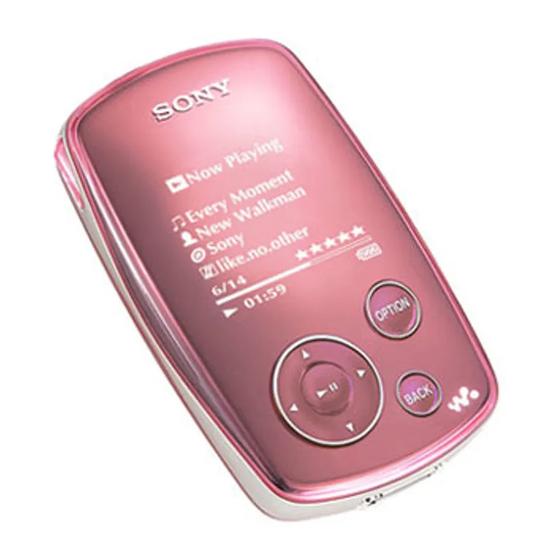
Also See for NW-A1000:
- User manual ,
- Operation manual (109 pages) ,
- Quick start manual (12 pages)
Table of Contents
Advertisement
SERVICE MANUAL
Ver. 1.2 2006.03
Sony Corporation
9-879-982-03
Connect Business Division
2006C05-1
Published by Sony Techno Create Corporation
© 2006.03
NW-A1000
SPECIFICATIONS
Audio compression technology
− MPEG-1 Audio Layer-3 (MP3)
− Adaptive Transform Acoustic Coding (ATRAC)
Maximum recordable number of track and time (Approx.)*
Bit rate
Tracks
Time
48 kbps
4,000
266 hours, 40 minutes
64 kbps
3,000
200 hours
96 kbps
2,000
133 hours, 20 minutes
128 kbps
1,500
100 hours
132 kbps
1,500
100 hours
160 kbps
1,200
80 hours
192 kbps
1,000
66 hours, 40 minutes
256 kbps
750
50 hours
320 kbps
600
40 hours
* When transferring four-minute tracks
Supported bit rates
MP3: 32 to 320 kbps (supports variable bite rate (VBR))
ATRAC: 48/64/66 (ATRAC3)*/96/105 (ATRAC3)*/128/132
(ATRAC3)/160/192/256/320 kbps
* You cannot record CDs in ATRAC3 format at 66 or 105 kbps using
CONNECT Player.
Sampling frequencies
MP3: 44.1 kHz
ATRAC: 44.1 kHz
S/N Ratio
Headphones: 84 dB or more
LINE OUT: 96 dB or more
Frequency response
20 to 20,000 Hz (single signal measurement during playback)
Output
i (headphones)/LINE OUT*: Stereo minijack/195 mV (10 Ω)
* The jack is used for both headphones and LINE OUT.
DIGITAL MUSIC PLAYER
US Model
Canadian Model
AEP Model
UK Model
Australian Model
Singapore Model
Korean Model
Operating temperature
5 to 35°C (41 to 95°F)
Power source
Built-in rechargeable battery DC IN 5 V
AC power adaptor: DC IN 5 V
Battery life (continuous playback)
In ATRAC format (48 kbps), Display 15 sec
Approx. 20 hours
In ATRAC format (128 kbps), Display 15 sec
Approx. 17 hours
In MP3 format (128 kbps), Display 15 sec
Approx. 17 hours
Dimension (w/h/d)
Approx. 55.0 88.1 18.7 mm (11.5 mm at thinnest point)*
(2 1/4 × 3 1/2 × 3/4 inches) (15/32 inches at thinnest point)*
* Not including projecting parts.
Dimension including projecting part (w/h/d)
Approx. 55.0 × 88.1 × 18.7 mm
(2 1/4 × 3 1/2 × 3/4 inches)
Mass
Approx. 109 g (3.9 oz)
Supplied Accessories
Headphones (1)
USB cable (1)
Headphone extension cord (1)
AC power cord (1)
AC power adaptor (1)
CD-ROM (1) (CONNECT Player software, Operation Guide
(PDF file))
Quick Start Guide (1)
Design and specifications are subject to change without notice.
US and foreign patents licensed from Dolby Laboratories.
Advertisement
Table of Contents

Related Manuals for Sony NW-A1000


Summary of Contents for Sony NW-A1000
-
Page 1: Specifications
(headphones)/LINE OUT*: Stereo minijack/195 mV (10 Ω) US and foreign patents licensed from Dolby Laboratories. * The jack is used for both headphones and LINE OUT. DIGITAL MUSIC PLAYER Sony Corporation 9-879-982-03 Connect Business Division 2006C05-1 Published by Sony Techno Create Corporation © 2006.03... -
Page 2: Table Of Contents
LES DIAGRAMMES SCHÉMATIQUES ET LA LISTE DES PIÈCES SONT CRITIQUES POUR LA SÉCURITÉ DE FONCTIONNEMENT. NE REMPLACER CES COM- POSANTS QUE PAR DES PIÈCES SONY DONT LES NUMÉROS SONT DONNÉS DANS CE MANUEL OU DANS LES SUPPLÉMENTS PUBLIÉS PAR SONY. -
Page 3: Servicing Notes
NW-A1000 Ver. 1.1 SECTION 1 SERVICING NOTES UNLEADED SOLDER NOTES ON REPLACEMENT OF HDD UNIT Boards requiring use of unleaded solder are printed with the lead- In this set, there are two kinds of HDD unit. (Refer to the figure free mark (LF) indicating the solder contains no lead. -
Page 4: General
NW-A1000 SECTION 2 This section is extracted from instruction manual. GENERAL... -
Page 5: Disassembly
NW-A1000 SECTION 3 DISASSEMBLY • This set can be disassembled in the order shown below. 3-1. DISASSEMBLY FLOW 3-2. CASE (LOWER) (Page 5) 3-3. LITHIUM ION BATTERY (Page 6) 3-4. CABINET (INNER) (Page 6) 3-5. EL BLOCK SUB ASSY (Page 7) 3-6. -
Page 6: Lithium Ion Battery
NW-A1000 4 two screws 2 two screws 3-3. LITHIUM ION BATTERY (B1.4) (B1.4) 6 connector (CN9001) 3 bracket (HDD) 7 lithium ion battery hole 1 two sheets (electrostatic CU) Note: Do not close the hole of bracket (HDD) when you paste the sheets (electrostatic CU). -
Page 7: El Block Sub Assy
NW-A1000 1 sheet 3-5. EL BLOCK SUB ASSY 2 Remove sheet (electric static G) (electrostatic CU) 2 Remove sheet (electrostatic CU) 4 two step screws 1 sheet (electric static G) boss 3 button assy 9 EL block sub assy 5 two step screws... -
Page 8: Position Of Ferrite Core
NW-A1000 Ver. 1.2 3-7. POSITION OF FERRITE CORE -AC POWER CORD- A cable is rolled onece. clamp filter (ferrite core) (Part No. : 1-500-386-11) -
Page 9: Test Mode
NW-A1000 SECTION 4 TEST MODE Checking method: Note: Information on the test mode must correspond in enough security. 1. Enter the test mode. When the leakage has been revealed by any chance, the source of 2. Press the [ ]... - Page 10 NW-A1000 5-1-2. Consumption current (read state) check 5-1-3. Consumption current (write state) check This mode is used in case consumption current (read state) in the This mode is used in case consumption current (write state) in the state where the hard disk drive has booted is checked.
- Page 11 NW-A1000 5-2. Audio 5-2-3. Frequency characteristic check While playing the audio track, it's in a repeat state. If [BACK] key is “20 Hz/20 kHz/100 Hz/10 kHz 0 dBs L-ch/R-ch VOLUME: 21” pressed, it’s stopped. audio signal is outputted. Press the [VOL +] key to switch the HP/LINE.
- Page 12 NW-A1000 13. Press the [ 3. Press the [ ] key to display minor item, and press the [ ] / [ ] key, “START” is displayed and “100 kHz 0 dBs L-ch/R-ch VOLUME: 21” audio signal is outputted. key to select the “MAXOUT”.
- Page 13 NW-A1000 5-2-7. BEEP check 9. Press the [ ] / [ ] key to select the “EQ 3”. BEEP sound is outputted. EL display Checking method: EQ 3 1. Enter the test mode. 2. Press the [ ] key to display major item, and press the [ ] / [ ] key to select the “AUDIO”.
- Page 14 NW-A1000 5-3. Others 5-3-2. Clock check 5-3-1. G-sensor check Clock operation is checked. X/Y/Z-axis direction is checked. Checking method: Checking method: 1. Enter the test mode. 2. Press the [ ] key to display major item, and press the [ ] / [ ] 1.
- Page 15 NW-A1000 4. Press the [ 10. Press the [ key, START” is displayed and EL display key, monochrome lattice is displayed on the EL. 11. Press the [BACK] key, return to minor item selection screen. corresponding to the pressed key is performed.
- Page 16 NW-A1000 8. “+X” is displayed. Main unit is fixed so that 1 of fig.1 may 5-3-6. G-sensor adjustment check become downward and press the [ key. This mode checks that G-sensor adjustment is performed or not performed. EL display Checking method: 1.
- Page 17 NW-A1000 4. Press the [ 5-3-7. Hard disk drive sector read key, “READY?” is displayed. Sector of hard disk drive is read. EL display Checking method: READY? 1. Enter the test mode. 2. Press the [ ] key to display major item, and press the [ ] / [ ] key to select the “OTHERS”.
- Page 18 NW-A1000 5-3-9. Destination setting 5-3-11. Sound pressure regulation setting Setting the destination. Setting the sound pressure regulation. Setting method: Setting method: 1. Enter the test mode. 1. Enter the test mode. 2. Press the [ ] key to display major item, and press the [ ] / [ ] 2.
- Page 19 NW-A1000 5-3-13. SDRAM check SDRAM is checked. Checking method: 1. Enter the test mode. 2. Press the [ ] key to display major item, and press the [ ] / [ ] key to select the “OTHERS”. EL display OTHERS 3.
-
Page 20: Diagrams
NW-A1000 SECTION 5 DIAGRAMS 5-1. BLOCK DIAGRAM – MAIN Section (1/2) – DATA BUS ADDRESS BUS SIGNAL PATH USB CONTROLLER MAIN SYSTEM CONTROLLER : AUDIO IC5001 IC6005 (1/2) HARD DISK DRIVE UNIT (6GB) SDATAO2, SCLK2, D24 – D31 D16 – D31... -
Page 21: Block Diagram - Main Section (2/2)
NW-A1000 5-2. BLOCK DIAGRAM – MAIN Section (2/2) – CN9201 (2/3) CRADLE CHARGE CRADLE ON/OFF SWITCH Q1002, 2002 DOG SPEAKER Q3007 J301 D/A CONVERTER AUDIO AMP IC3002 IC3003 SDATAO2, SCLK2, LRCK2, FS256 SDATAO2 (Page 20) DATA VOUTL 7 L-IN LOUT 12... -
Page 22: Block Diagram - Power Supply Section
NW-A1000 5-3. BLOCK DIAGRAM – POWER SUPPLY Section – CN9201 (3/3) CRADLE_SO 71 CRADLE_SI 7 CRADLE_SCK 5 SCLK CRADLE_CS 14 CRDL_ DET ADP_DET 77 ADP_DET JACK_DET 58 LINE_DET RM_KEY CHG_LED POWER CONTROL, CHARGE CONTROL IC9001 CHARGE CRADLE CHARGE SWITCH XCHG_STAT1... - Page 23 NW-A1000 • Note for Printed Wiring Boards and Schematic Diagrams • Waveforms Note on Printed Wiring Board: Note on Schematic Diagram: • X : parts extracted from the component side. • All capacitors are in µF unless otherwise noted. (p: pF)
-
Page 24: Main Board (Component Side)
NW-A1000 5-4. PRINTED WIRING BOARD – MAIN Board (Component Side) – :Uses unleaded solder. MAIN BOARD (COMPONENT SIDE) S8302 D8304 TP9027 TP9026 TP9028 TP5001 TP8032 TP8068 (1.10V) (1.8V) (3.3V) TP9029 D8304, S8302 LINK TP9025 TP8304 TP8098 SP9019 TP8307 SP9023 SP9004... -
Page 25: Main Board (Conductor Side)
NW-A1000 5-5. PRINTED WIRING BOARD – MAIN Board (Conductor Side) – :Uses unleaded solder. EL MODULE SWITCH MAIN BOARD (CONDUCTOR SIDE) UINT VDR3104 R3107 R3116 VDR3102 R8306 C5021 R3108 R3106 L9003 R5015 R3110 CN8302 C9004 C3101 VDR3101 VDR3103 X3101 HARD... -
Page 26: Schematic Diagram - Main Board (1/8)
NW-A1000 • See page 23 for Waveforms. • See page 34 for IC Block Diagrams. • See page 36 for IC Pin Function Description. 5-6. SCHEMATIC DIAGRAM – MAIN Board (1/8) – (1/8) FRES_XWE AF_XRST FRES_XWE AF_XRST FRES_XCAS FRES_RXW FRES_XCAS... -
Page 27: Schematic Diagram - Main Board (2/8)
NW-A1000 5-7. SCHEMATIC DIAGRAM – MAIN Board (2/8) – (2/8) RDY_XBUSY FRES_D<31:16> AF_XRST FRES_RXW IC7001 EDS1216AABH-75-E ∗ SD-RAM FRES_A17 (Page 26) CSP(Chip Size Package) C7007 C7008 NOR FLASH MEMORY CSP(Chip Size Package) IC7002 FRES_D16 FRES_D31 DQ15 S29PL032J60BFI120 FRES_A16 C7009 C7004... -
Page 28: Schematic Diagram - Main Board (3/8)
NW-A1000 • See page 34 for IC Block Diagrams. 5-8. SCHEMATIC DIAGRAM – MAIN Board (3/8) – (3/8) TP8303 CN8301 C8301 C8302 C8321 HOLD_KEY XRESET_LCD XRESET_LCD LCD_DC LCD_DC FRES_RXW FRES_RXW FRES_XOE FRES_XOE (Page 26) DC/DC CONVERTER IC8301 R8303 TPS61045 IREF... -
Page 29: Schematic Diagram - Main Board (4/8)
NW-A1000 • See page 36 for IC Pin Function Description. 5-9. SCHEMATIC DIAGRAM – MAIN Board (4/8) – (4/8) AF_DCIN_DET AF_DCIN_DET (Page 26) PWR_FFCLR PWR_FFCLR SCLK1 SCLK1 LRCK1 R8017 LRCK1 MULTI_SI C8024 MULTI_SI MULTI_SCK MULTI_SCK SDATAO1 SDATAO1 MULTI_SO R8016 C8023... -
Page 30: Schematic Diagram - Main Board (5/8)
NW-A1000 • See page 23 for Waveforms. • See page 34 for IC Block Diagrams. • See page 36 for IC Pin Function Description. 5-10. SCHEMATIC DIAGRAM – MAIN Board (5/8) – (5/8) X3101 22.5792MHz C3112 R4204 220k C3107 L3101... -
Page 31: Schematic Diagram - Main Board (6/8)
NW-A1000 • See page 23 for Waveforms. • See page 34 for IC Block Diagrams. 5-11. SCHEMATIC DIAGRAM – MAIN Board (6/8) – (6/8) R3044 R3040 R3038 3.0V IC3001 XC6219B282DR F3001 3.3V_A 0.25A 125V 1.8V C3034 VOUT R3001 R3033 GND_A (Page 32) 5.0V... -
Page 32: Schematic Diagram - Main Board (7/8)
NW-A1000 5-12. SCHEMATIC DIAGRAM – MAIN Board (7/8) – • See page 36 for IC Pin Function Description. (7/8) XRST (Page 26) XRST PWR_FFCLR R9047 PWR_FFCLR PWR_SLEEP PWR_SLEEP XVBUS_LIM XVBUS_LIM R9043 470k BAT_MON_CTL R9066 R9041 BAT_MON_CTL Q9005,9009 R9062 R9056 R9058... -
Page 33: Schematic Diagram - Main Board (8/8)
NW-A1000 5-13. SCHEMATIC DIAGRAM – MAIN Board (8/8) – • See page 23 for Waveforms. • See page 36 for IC Pin Function Description. (Page 29) (Page 26) (Page 31) (Page 32) (Page 32) (8/8) CN9201 R5052 FB5006 C5012 FB5001... - Page 34 NW-A1000 • IC Block Diagrams IC3001 XC6219B302DR IC4101 R2061K01-E2 VIN 1 9 /INTR ON/OFF NC 2 LEVEL CONTROL SIO 1 SHIFTER SCLK 2 8 OSCOUT REAL VOUT 3 TIME VOLTAGE CLOCK REFERENCE /VDCC 3 CURRENT 7 OSCIN LIMIT – DELAY...
- Page 35 NW-A1000 IC8301 TPS61045DRBR INPUT SWITCH UNDER VOLTAGE GATE LOCKOUT CTRL 400 ns MIN DRIVER BIAS SUPPLY OFF TIME MAIN ERROR COMPARATOR SWITCH 8 SW – GATE RS LATCH DRIVER LOGIC VREF 6 µs MAX ON TIME CURRENT LIMIT – PGND...
- Page 36 NW-A1000 • IC Pin Function Description IC3101 CXR710160-215GH (SUB SYSTEM CONTROLLER) Pin No. Pin Name Description LRCK L/R sampling clock signal input from the PLD Bit clock signal input from the PLD VDIOCD0 Power supply terminal (+1.8V) (for CD interface and I/O)
- Page 37 NW-A1000 Pin No. Pin Name Description 50, 51 TEST6, TEST5 Output terminal for the test 52 to 55 TEST4 to TEST1 Input terminal for the test DVDD3 Power supply terminal (+1.3V) DVSS1 Ground terminal TEST0 Input terminal for the test...
- Page 38 NW-A1000 IC5001 S1R72003BOOA100 (USB CONTROLLER) Pin No. Pin Name Description Internal operation setting terminal N.C. Not used AVSS Ground terminal (analog system) AVDD Power supply terminal (+3.3V) (analog system) AVSS Ground terminal (analog system) AVDD Power supply terminal (+3.3V) (analog system)
- Page 39 NW-A1000 Pin No. Pin Name Description HIORDY Wait signal input from the hard disk drive unit Ground terminal (logic system) Power supply terminal (+3.3V) (logic system) XHDMACK DMA acknowledge signal output to the hard disk drive unit HINTRQ Interrupt request signal input from the hard disk drive unit...
- Page 40 NW-A1000 IC6005 SCF5250 (MAIN SYSTEM CONTROLLER) Pin No. Pin Name Description DATA16 Two-way data bus with the SD-RAM and NOR flash memory Address signal output to the SD-RAM PAD_VDD Power supply terminal (+3V) (for I/O) Address signal output to the SD-RAM...
- Page 41 NW-A1000 Pin No. Pin Name Description PAD_GND Ground terminal (for I/O) SCLK1 Bit clock signal input from the PLD LRCK1 L/R sampling clock signal input from the PLD SDATAO1 Audio data output to the PLD TSB_XLT TSB latch signal output terminal Not used...
- Page 42 NW-A1000 Pin No. Pin Name Description LINOUT Not used LININ Not used CORE_VDD Power supply terminal (+1.1V) (for core) SDATAO2 Audio data output to the D/A converter Not used Hi-Z Not used 115 to 117 TEST0 to TEST2 Input terminal for the test mode setting...
- Page 43 NW-A1000 IC8001 LC4128ZC-75MN132C-U5 (PLD) Pin No. Pin Name Description Ground terminal Data input terminal (for JTAG) Not used VCCIO0 Power supply terminal (+3V) (for I/O) EX_MULTI_SCK Serial data transfer clock signal output to the real time clock and power control...
- Page 44 NW-A1000 Pin No. Pin Name Description VCCIO0 Power supply terminal (+3V) (for I/O) CRD_MUTE1 Headphone/cradle selection signal output for audio output "L": headphone, "H": cradle RESET_TSB TSB reset signal output terminal Not used Headphone/cradle selection signal output for audio output to the audio amplifier HP_LINE_SEL "L": cradle, "H": headphone...
- Page 45 NW-A1000 Pin No. Pin Name Description SDATAO1 Audio data input from the main system controller GNDIO1 Ground terminal (for I/O) MULTI_SO Serial data input from the main system controller DEN_SI0 Serial data output to the sub system controller WAKEUP_DEN Wake-up signal output to the sub system controller...
- Page 46 NW-A1000 IC9001 uPD68855F9-Y03-BA2-E2-A (POWER CONTROL, CHARGE CONTROL) Pin No. Pin Name Description Power supply output terminal (+1.1V) Power supply output terminal (+1.8V) 3, 4 Power supply output terminal (+3.3V) Power supply output terminal (+5V) VO4-2 Power supply output terminal Not used DCDC4EN Power on/off control signal input for VO4 "H": power on...
- Page 47 NW-A1000 Pin No. Pin Name Description CRST1 External capacitor connection terminal for reset delay (for XRST1) CRST2 External capacitor connection terminal for reset delay (for XRST2) CRST3 External capacitor connection terminal for reset delay (for XRST3) LDO output trigger selection signal input terminal "L": VO interlock, "H": XRST interlock SEQSEL Fixed at "L"...
-
Page 48: Exploded View
NW-A1000 Ver. 1.1 SECTION 6 EXPLODED VIEWS NOTE: • -XX and -X mean standardized parts, so they • Items marked “*” are not stocked since they may have some difference from the original are seldom required for routine service. Some one. -
Page 49: Main Section
NW-A1000 Ver. 1.1 6-2. MAIN SECTION (AEP, UK, SP, KR) (AEP, UK, SP, KR) Note: Refer to Servicing Notes "note on replacement of HDD unit" (3 page) when you exchange HDD unit (Ref. No. 64). Ref. No. Part No. Description Remark Ref. -
Page 50: Electrical Parts List
NW-A1000 Ver. 1.1 SECTION 7 MAIN ELECTRICAL PARTS LIST NOTE: • Due to standardization, replacements in the • Items marked “*” are not stocked since they The components identified by mark 0 or dotted line with mark 0 are parts list may be different from the parts are seldom required for routine service. - Page 51 NW-A1000 MAIN Ref. No. Part No. Description Remark Ref. No. Part No. Description Remark C5019 1-100-504-11 CERAMIC CHIP 0.1uF 6.3V C6055 1-100-504-11 CERAMIC CHIP 0.1uF 6.3V C5020 1-100-504-11 CERAMIC CHIP 0.1uF 6.3V C6056 1-100-506-11 CERAMIC CHIP 6.3V C6057 1-128-617-11 CERAMIC CHIP...
- Page 52 NW-A1000 MAIN Ref. No. Part No. Description Remark Ref. No. Part No. Description Remark C8311 1-162-915-11 CERAMIC CHIP 10PF 0.5PF D9001 6-500-483-01 DIODE MA22D2800LS0 C8312 1-127-760-11 CERAMIC CHIP 4.7uF 6.3V D9002 6-501-286-01 DIODE MA22D3900LS0 C8314 1-125-777-11 CERAMIC CHIP 0.1uF D9003...
- Page 53 NW-A1000 MAIN Ref. No. Part No. Description Remark Ref. No. Part No. Description Remark @ IC8001 6-805-984-03 IC LC4128ZC-75MN132C-U5 IC8301 6-708-817-01 IC TPS61045DRBR R1008 1-218-961-11 RES-CHIP 4.7K 1/16W IC8302 6-707-529-01 IC TPS61041DBVR R1009 1-218-977-11 RES-CHIP 100K 1/16W @ IC9001 6-708-829-01 IC uPD68855F9-Y03-BA2-E2-A...
- Page 54 NW-A1000 MAIN Ref. No. Part No. Description Remark Ref. No. Part No. Description Remark R5002 1-218-977-11 RES-CHIP 100K 1/16W R5003 1-208-905-11 METAL CHIP 5.6K 0.5% 1/16W R6014 1-218-990-11 SHORT CHIP R5004 1-218-977-11 RES-CHIP 100K 1/16W R6015 1-218-990-11 SHORT CHIP R6016...
- Page 55 NW-A1000 MAIN Ref. No. Part No. Description Remark Ref. No. Part No. Description Remark R8026 1-218-965-11 RES-CHIP 1/16W R8027 1-218-965-11 RES-CHIP 1/16W R9002 1-219-797-11 METAL CHIP 0.33 1/4W R8028 1-218-965-11 RES-CHIP 1/16W R9003 1-218-953-11 RES-CHIP 1/16W R9004 1-218-961-11 RES-CHIP 4.7K...
- Page 56 NW-A1000 Ver. 1.2 MAIN Ref. No. Part No. Description Remark Ref. No. Part No. Description Remark < THERMISTOR > ACCESSORIES ************ TH9001 1-804-949-11 THERMISTOR, NTC (SMD) TH9002 1-805-719-11 THERMISTOR, POSITIVE 1-479-577-21 ADAPTOR, AC (AC-S508U) (US, CND) 1-479-577-31 ADAPTOR, AC (AC-S508U) (AEP, UK, SP) <...
- Page 57 NW-A1000 MEMO...
-
Page 58: Revision History
NW-A1000 REVISION HISTORY Clicking the version allows you to jump to the revised page. Also, clicking the version at the upper right on the revised page allows you to jump to the next revised page. Ver. Date Description of Revision 2005.11...