
Related Manuals for LG MAX220UB


Summary of Contents for LG MAX220UB
-
Page 1: Service Manual
Internal Use Only Website http://biz.lgservice.com DIGITAL MEDIA RECEIVER SERVICE MANUAL MODEL: MAX220UB CAUTION BEFORE SERVICING THE UNIT, READ THE “SAFETY PRECAUTIONS” IN THIS MANUAL. P/NO : AFN75741202 MARCH, 2012... -
Page 2: Table Of Contents
CONTENTS SECTION 1 SUMMARY SERVICING PRECAUTIONS ..........................1-2 ESD PRECAUTIONS ............................1-3 SPECIFICATIONS ..............................1-4 LOCATION OF USERS CONTROLS .........................1-5 HOW TO SETTING THE OPTION CODE ......................1-6 FIRMWARE UPGRADE METHOD ........................1-7 HOW TO CONNECT AUDIO SET TO POWER SUPPLY ..................1-8 SECTION 2 ELECTRICAL ELECTRICAL TROUBLESHOOTING GUIDE ....................2-1 1. -
Page 3: Servicing Precautions
SECTION 1 SUMMARY SERVICING PRECAUTIONS 1. Always disconnect the power source before: 1) Removing or reinstalling any component, circuit board, module or any other instrument assembly. 2) Disconnecting or reconnecting any instrument electrical plug or other electrical connection. 3) Connecting a test substitute in parallel with an electrolytic capacitor in the instrument. CAUTION: A wrong part substitution or incorrect polarity installation of electrolytic capacitors may result in an explosion hazard. -
Page 4: Esd Precautions
ESD PRECAUTIONS Electrostatically Sensitive Devices (ESD) Some semiconductor (solid state) devices can be damaged easily by static electricity. Such components com- monly are called electrostatically sensitive devices (ESD). Examples of typical ESD devices are integrated circuits and some fi eld-effect transistors and semiconductor chip components. The following techniques should be used to help reduce the incidence of component damage caused by static electricity. -
Page 5: Specifications
SPECIFICATIONS • General Output Power 53 W x 4 CH (Max.) Power Source DC 12 V Speaker impedance 4 Ω Ground System Negative Dimensions (W x H x D) 178 x 50 x 168 mm (without Control Panel) Net Weight 0.97 kg •... -
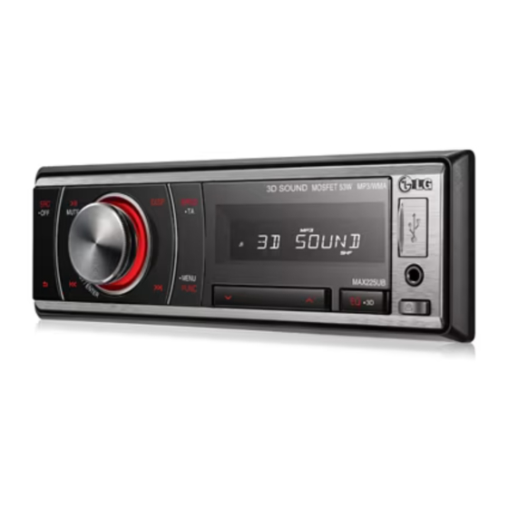
Page 6: Location Of Users Controls
LOCATION OF USERS CONTROLS FRONT PANEL A SRC / • OFF - When pressed, selects function sources. Skip / Search / Seek / Tune - When pressed and held, powers unit on or off. K • MENU Activates setting menu. Plays and pauses playback. -
Page 7: How To Setting The Option Code
HOW TO SETTING THE OPTION CODE 1. Option Table Option Codes for Media Receiver products of 2012 will be defi ned as below * OPTION TABLE INDEX AREA OPTION CODE SUFFIX EDEULL* EDZALL* EESPLL* EHUNLL* SUPPORT EMARLL* ESWELL* ETUREL* EZAFLL* SUPPORT ERUSLL* EINDLL*... -
Page 8: Firmware Upgrade Method
FIRMWARE UPGRADE METHOD [ MAIN AND CD FIRMWARE UPGRADE ] 1. Confi rmation of version information • Change the Source of audio set to tuner. (Default: tuner) • Turn power off using power key. • Press power key for 5 s. (After power on, continue pressing) •... -
Page 9: How To Connect Audio Set To Power Supply
HOW TO CONNECT AUDIO SET TO POWER SUPPLY • It is suffi cient only to supply power for upgrade. • Shown from the right fi gure, connect yellow line (Battery) and red line (Ignition) to plus and minus terminal respectively. •... -
Page 10: Electrical Troubleshooting Guide
SECTION 2 ELECTRICAL ELECTRICAL TROUBLESHOOTING GUIDE 1. SYSTEM CONTROL ERROR CORRECTION FLOW CHART Something wrong with the System control? No power? Checked the Fuse? F301 Inside of JK801 Checked the Back up JK801(1, 2, 3, 4) VDD and GND? Checked the Regulator IC801(15, 14) Back up VDD? Checked the Main Micom... - Page 11 [OPTIONAL] Not available to Remocon? Checked the RC902, R961 Remocon Sense VDD? Checked the R962, IC401(7), CN402(11) Remocon Sense line? Not available to Volume control? Checked the EV901, IC401(6, 68), CN402(14, 15) Encoder volume? Checked the IC401(31, 32), IC601(25, 26) Volume IC control? Not available to Key control? Checked the...
- Page 12 Not available to ANT(Motor Type) control? Checked the D808, IC801(6, 11), IC401(94) ANT control? [OPTIONAL] Not available to Remote(External AMP) control? JK801(9), IC401(84), Checked the Q811, Q812, Q813 Remote control?
-
Page 13: Sound Error Correction Flow Chart
2. SOUND ERROR CORRECTION FLOW CHART Something wrong with the Sound? No sounds of All Functions? Checked the IC601(24) E-VR VDD? Checked the IC601(27) E-VR GND? Checked the IC601(25, 26), IC401(31, 32) E-VR control? Checked the E-VR IC601(15), IC401(98) Mute control? IC601(1, 2, 3, 4, 5, 6, 7, 9, Checked the E-VR 18, 19, 20, 21, 22, 23) - Page 14 Hearing the Pop Noise? IC401(87, 96, 98), IC601(15), IC804(22), Checked the Q601, Q602, Q603, Q604, Q607 Mute contorl? [OPTIONAL] No Sound External AMP? Checked the IC601(18, 19, 20, 21, 22, 23) Line Out signal? Checked the Line Out Q601, Q602, Q603, Q604, Q607 AMP Mute control? Checked the Line Out JK601...
- Page 15 CAUTION - Tip for repair Before exchange power amp IC(TB2931) for no audio problem, you have to check below list. 1. Check VCC (pin 20, 6) & GND 2. Check input pin 11, 12, 14, 15 Ripple Out1 (+) 3. Check Standby, pin 4 PW-GND1 : Follow the below list.
-
Page 16: Display Error Correction Flow Chart
3. DISPLAY ERROR CORRECTION FLOW CHART Something wrong with the Display? No Display or Some Display is broken? Checked the LCD IC901(56) Driver Vdd? Checked the LCD IC901(60) Driver Ground? Checked the LCD IC901(57), IC401(29) Driver RESET? Checked the LCD IC901(61) Driver OSC? IC401(23, 24, 25, 29),... -
Page 17: Tuner Error Correction Flow Chart
4. TUNER ERROR CORRECTION FLOW CHART Something wrong with the Tuner system? Not available to Tuner? Checked the IC101(6, 22) Tuner VDD? Checked the Tuner IC801(4, 5), IC401(95), D817 VDD control? Checked the IC101(5, 10, 17, 23) Tuner GND? Checked the E-VR IC601(15), IC401(98) Mute control? Checked the... -
Page 18: Usb Error Correction Flow Chart
5. USB ERROR CORRECTION FLOW CHART Something wrong with the USB? Only "NO USB" or "USB CHECK" Display? IC805, IC401(52) Checked the USB VDD? IC501(4, 5, 7, 9, 12, 44, 49, 51, 74, 77, 81, Checked the USB interface IC GND? 102, 104, 116, 117) Checked the USB IC401(42), R425... - Page 19 "FILE CHECK" Display? IC501(4, 5, 7, 9, 12, 44, 49, 51, 74, 77, 81, Checked the CD DSP GND? 102, 104, 116, 117) Checked the USB IC401(42), R425 interface IC reset? Checked the X502 DSP X-tal? Checked the IC401(26, 27, 28, 60) DSP control? USB no sound? Checked the CD...
-
Page 20: Aux Error Correction Flow Chart
6. AUX ERROR CORRECTION FLOW CHART Something wrong with the AUX? AUX no sound? JK903, IC601(7, 9), CN971(19, 20, 21), Checked the AUX CN402(4, 5, 6) Signal input? Checked the See the Sound Error correction Process. E-VR & Power AMP? 2-11... -
Page 21: Waveforms
WAVEFORMS 1) MICOM(IC401) ↔ DISPLAY(CN402) IC401:[PIN25] IC401:[PIN23] IC401:[PIN24] IC401:[PIN29] 2) MICOM(IC401) ↔ TUNER IC(IC101) IC401:[PIN2] IC401:[PIN1] 3) MICOM(IC401) ↔ VOLUME IC(IC601) IC401:[PIN32] IC401:[PIN31] 2-12... -
Page 22: Circuit Voltage Chart
CIRCUIT VOLTAGE CHART IC101 IC601 IC801 Voltage PIN NAME Voltage PIN NAME Voltage PIN NAME AM Mode FM Mode 4.183 8.42 AMRFIN 2.884 4.185 AMRFDEC 4.175 4.184 CD 8 V FMIN2 4.184 CTL1 4.661 FMIN1 4.18 AUDIO 8.4 V 8.43 GNDRF 4.18 CTL2... -
Page 23: Internal Block Diagram Of Ics
INTERNAL BLOCK DIAGRAM OF ICs 1. IC601 (BD3702FV) 1-1. BLOCK DIAGRAM 1-2. PIN DESCRIPTION Terminal Terminal Terminal Terminal Description Description Name Name A input terminal of 1ch MUTE External compulsory mute terminal A input terminal of 2ch LRST Level meter reset terminal B input terminal of 1ch LOUT Output terminal for Level meter... -
Page 24: Ic801 (Lv5693P)
2. IC801 (LV5693P) 2-1. BLOCK DIAGRAM V CC AMP_HS-SW(V CC -1 V) Over 500 mA Start Voltage Protection Vref ILM output (8.4 V) 500 mA AUDIO output (8.4 V) CTRL1 500 mA OUTPUT V CC CTRL2 Control Ilim Recommendation FET:2SJ650 CTRL3 USB output (5 V) 1000 mA... -
Page 25: Pin Description
2-2. PIN DESCRIPTION Pin No. Pin name Description ILM output pin ON when CTRL2 = M1, H 8.4 V/ 0.5 A GND pin CD output pin ON when CTRL1 = H 8.0 V/ 1.3 A CTRL1 input pin CTRL1 Three value input AUDIO output pin AUDIO ON when CTRL1 = M, H... -
Page 26: Ic804 (Tb2931Hq)
3. IC804 (TB2931HQ) 3-1. BLOCK DIAGRAM Ripple Out1 (+) PW-GND1 Out1 (−) Out2 (+) PW-GND2 Pre-GND Out2 (−) Out3 (+) PW-GND3 Out3 (−) AC-GND Out4 (+) PW-GND4 4 Stby Out4 (−) Play Mute 22 Mute Offset/short 2-17... - Page 27 2-18...
-
Page 28: Wiring Diagram
WIRING DIAGRAM B+, ACC, Speaker out, Power Antenna, External AMP Remote (Optional) (Optional) LINEOUT POWER 4 CH HARNESS SK101 17PIN 11PIN Wired 3PIN CONNECTOR CONNECTOR Remocon CONNECTOR (Optional) CN404 CN502 CN501 CN402 24PIN MAIN BOARD CONNECTOR 24PIN 1LINE LCD CONNECTOR Jack JK903 CN971... -
Page 29: Block Diagrams
BLOCK DIAGRAMS 1. MAIN BLOCK DIAGRAM OPTIONAL MULTI-Reg WIRED POWER SANYO LINE-OUT (ATS-L03) 16PIN LV5693P JACK FM/AM RF SIGNAL FL/FR/RL/RR 4 CH Audio Power IC TB2931HQ TUNER_L/R TUNER NXP OUT_F/OUT_R OUT_F/OUT_S (TEF6624) VOL IC DSP L/R (BD37C007FV) L/R PWM CHIP PCM 1808 MICOM TAMUL... -
Page 30: Front Block Diagram
2. FRONT BLOCK DIAGRAM OPTIONAL LED DRIVER IC 3-color LED VOL UP/DOWN (AAT3129) Encoder KEY LED(GREEN) ADC KEY1/KEY2 Tact SW KEY LED(RED) REMOCON LCD BLU LCD BLU WHITE LED AUX R/L JACK D+/D- SOCKET LCD Driver IC (MC5502) Detachable 24PIN/ Flip-Down 30PIN CONNECTOR 2-23 2-24... -
Page 31: Electrical Block Diagram
3. ELECTRICAL BLOCK DIAGRAM OPTIONAL ACTIVE_LOW ACC DET LOW/HIGH OVP BATT DET VOLUME IC BD3702FV POWER ACTIVE_HIGH ILLUMI 16PIN TUNER BA00CC0WFP REMOTE_ON (TEF6624T) 280uH Inductor B+(14.4 V) 4 CH Audio Power IC TB2931HQ BATT_12 V VDD 5 V MICOM VDD_5.7 V SANYO 300 mA (LC87F5WC8A) -
Page 32: Circuit Diagrams
CIRCUIT DIAGRAMS 1. MAIN_1 CIRCUIT DIAGRAM MAIN EAX64686601_7_1.3-SD(#1) 2012. 02. 07 2-27 2-28... -
Page 33: Main_2 Circuit Diagram
2. MAIN_2 CIRCUIT DIAGRAM MAIN EAX64686601_7_1.3-SD(#2) 2012. 02. 07 2-29 2-30... -
Page 34: Front Circuit Diagram
3. FRONT CIRCUIT DIAGRAM FRONT EAX64686001_7_1.4-SD 2012. 02. 07 2-31 2-32... -
Page 35: Printed Circuit Board Diagrams
PRINTED CIRCUIT BOARD DIAGRAMS 1. MAIN P.C.BOARD (TOP VIEW) (BOTTOM VIEW) 2-33 2-34... -
Page 36: Front P.c.board
2. FRONT P.C.BOARD (TOP VIEW) (BOTTOM VIEW) 2-35 2-36... - Page 37 2-37 2-38...
-
Page 38: Exploded Views
SECTION 3 EXPLODED VIEWS 1. CABINET AND MAIN FRAME SECTION Accessory Loc.No. Loc.No. Loc.No. Loc.No. LCD901 FRONT MAIN...