Table of Contents
Advertisement
Please refer to the original service manual for:
CD Mechanism Unit (BRS12C) , Order No. PSG1303059AE
Speaker system SB-AKX200LM, Order No. PMX1505004CE
Speaker system SB-AKX400LM, Order No. PMX1505005CE
TABLE OF CONTENTS
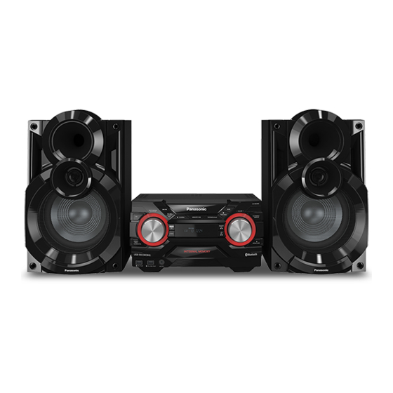
SA-AKX200LM
Model No.
SA-AKX400LM
Product Color: (K)...Black Type
prevention
© Panasonic Corporation 2015. All rights reserved.
Unauthorized copying and distribution is a violation
of law.
PMX1505003CE
CD Stereo System
electrostatic
breakdown
Advertisement
Table of Contents

Related Manuals for Panasonic SA-AKX200LM


Summary of Contents for Panasonic SA-AKX200LM
-
Page 1: Table Of Contents
2.3. General description about Lead Free Solder 6.2. Sales Demonstration Lock Function (PbF) 6.3. Doctor Mode Table 2.4. Handling Precautions for Traverse Unit 6.4. Self-Diagnostic Mode © Panasonic Corporation 2015. All rights reserved. Unauthorized copying and distribution is a violation of law. - Page 2 12.6. Main (Tuner AUX) Circuit 12.7. Main (DSP Bluetooth) Circuit 12.8. Main (Damp) Circuit 12.9. Main (Voltage Regulator) Circuit 12.10. Panel Circuit (For SA-AKX200LM) 12.11. Panel Circuit (For SA-AKX400LM) 12.12. USB, CD Interface and Music Port Circuit 13 Printed Circuit Board 13.1.
-
Page 3: Safety Precautions
1 Safety Precautions 1.1. General Guidelines 1. IMPORTANT SAFETY NOTICE There are special components used in this equipment which are important for safety. These parts are marked by in the Schematic Diagrams, Circuit Board Layout, Exploded Views and Replacement Parts List. It is essential that these critical parts should be replaced with manufacturer’s specified parts to prevent X-RADIATION, shock, fire, or other hazards. -
Page 4: Before Repair And Adjustment
Power Supply using SMPS Module This model uses Switching Mode Power Supply (SMPS Module) to provide the power supply to the unit. Here is the supplied part no. for the SMPS Module 1) N0AB1GK00001 (For SA-AKX200LM) 2) N0AB1GL00001 (For SA-AKX400LM) - Page 5 1.4.1. For SA-AKX200LM Figure 1-3 1.4.2. For SA-AKX400LM Figure 1-4...
-
Page 6: Safety Parts Information
1.5. Safety Parts Information Safety Parts List: There are special components used in this equipment which are important for safety. These parts are marked by in the Schematic Diagrams, Exploded View & Replacement Parts List. It is essential that these critical parts should be replaced with manufacturer’s specified parts to prevent shock, fire or other hazards. -
Page 7: Warning
2 Warning 2.1. Prevention of Electrostatic Discharge (ESD) to Electrostatically Sensi- tive (ES) Devices Some semiconductor (solid state) devices can be damaged easily by static electricity. Such components commonly are called Elec- trostatically Sensitive (ES) Devices. The following techniques should be used to help reduce the incidence of component damage caused by electrostatic discharge (ESD). -
Page 8: General Description About Lead Free Solder (Pbf)
2.3. General description about Lead Free Solder (PbF) The lead free solder has been used in the mounting process of all electrical components on the printed circuit boards used for this equipment in considering the globally environmental conservation. The normal solder is the alloy of tin (Sn) and lead (Pb). On the other hand, the lead free solder is the alloy mainly consists of tin (Sn), silver (Ag) and Copper (Cu), and the melting point of the lead free solder is higher approx.30 degrees C (86°F) more than that of the normal solder. -
Page 9: Grounding For
ble cable, cut off the antistatic FFC. Figure 2-2 2.5. Grounding for electrostatic breakdown prevention • As for parts that use optical pick-up (laser diode), the optical pick-up is destroyed by the static electricity of the working environ- ment. Repair in the working environment that is grounded. 2.5.1. -
Page 10: Service Navigation
3 Service Navigation 3.1. Service Information This service manual contains technical information which will allow service personnel’s to understand and service this model. Please place orders using the parts list and not the drawing reference numbers. If the circuit is changed or modified, this information will be followed by supplement service manual to be filed with original service manual. -
Page 11: Specifications
4 Specifications Speaker section For AKX200 Amplifier section Type 2 way, 2 speaker system RMS output power stereo mode Speaker unit(s) Front Ch (both ch driven) 200 W per channel (4 Ω),1 kHz, 30% THD (for AKX200) Woofer 16 cm cone type 300 W per channel (3 Ω),1 kHz, 30% THD (for AKX400) Tweeter 6 cm cone type... -
Page 12: Location Of Controls And Components
5 Location of Controls and Components 5.1. Remote Control Key Button Operation 5.1.1. For SA-AKX200 5.1.2. For SA-AKX400... -
Page 13: Main Unit Key Button Operation
5.2. Main Unit Key Button Operation 5.2.1. For SA-AKX200... - Page 14 5.2.2. For SA-AKX400...
-
Page 15: Service Mode
6 Service Mode 6.1. Cold-Start Item Key Operation FL Display Mode Name Description Front Key Cold Start To carry out cold-start or initialize 1. Unplug AC power cord. to shipping mode 2. Press & hold [POWER] button. 3. Plug in AC power cord while [POWER] button being pressed. -
Page 16: Doctor Mode Table
6.3. Doctor Mode Table 6.3.1. Doctor Mode Table 1 Item Key Operation FL Display Mode Name Description Front Key Doctor Mode 1. Press [ ] button on main unit follow by [4] and [7] on remote control. 2. To exit, press [DELETE] button on remote control or, press [POWER, /I] button on Main Unit... - Page 17 6.3.2. Doctor Mode Table 2 Item Key Operation FL Display Mode Name Description Front Key Volume Setting To check the volume setting of the In Doctor Mode: Check main unit. 1. Press [7], [8], [9] button on the remote control. Press [7]: VOL50 Volume Press [8]: VOL35...
-
Page 18: Self-Diagnostic Mode
6.4. Self-Diagnostic Mode Item Key Operation FL Display Mode Name Description Front Key Self Diagnostic To enter into self diagnostic checking Step 1: Select CD mode Mode (Ensure no disc is inserted). Step 2: Press & hold [ ] button follow by [ ] on main unit for 2 seconds. - Page 19 6.5.2. CD Mechanism Error Code Table Item Key Operation FL Display Mode Name Description Front Key Error Code Diagnosis Contents: Press [ ] on main unit for next CD H15 CD Open Abnormal error. During operation POS_SW_R On fail to be detected within 4 sec. Error No.
-
Page 20: Troubleshooting Guide
7 Troubleshooting Guide “Contents for this section is not available at time of issue”... -
Page 21: Disassembly And Assembly Instructions
8 Disassembly and Assembly Instructions • Illustration is based on SA-AKX400LM. Caution Note: • This section describes the disassembly and/or assembly procedures for all major printed circuit boards & main compo- nents for the unit. (You may refer to the section of “Main components and P.C.B Locations” as described in the service manual) •... -
Page 22: Disassembly Flow Chart
8.2. Disassembly Flow Chart Top Cabinet Front Panel Unit Rear Panel Main P.C.B. Panel P.C.B. SMPS Module USB P.C.B. Music Port P.C.B. (For AKX400) CD Mechanism Unit CD Interface P.C.B. 8.3. Main Components and P.C.B. Locations... -
Page 23: Disassembly Of Top Cabinet
8.4. Disassembly of Top Cabinet Step 5 Slightly lift up to remove Top Cabinet. Step 1 Remove 2 screws. Step 2 Remove 2 screws. 8.5. Disassembly of Front Panel Unit • Refer to “Disassembly of Top Cabinet”. Step 1 Lift up Wire Clampers. Step 2 Detach 17P FFC at connector (CN2500) on Main P.C.B.. -
Page 24: Disassembly Of Panel P.c.b
8.6. Disassembly of Panel P.C.B. Step 5 Release tabs at bottom of unit. • Refer to “Disassembly of Top Cabinet”. • Refer to “Disassembly of Front Panel Unit”. Step 1 Remove Volume Knob. Step 2 Remove Multi Control Knob. Step 3 Remove 2 screws. Step 4 Release catches. -
Page 25: Disassembly Of Usb P.c.b
8.7. Disassembly of USB P.C.B. 8.9. Disassembly of Rear Panel • Refer to “Disassembly of Top Cabinet”. • Refer to “Disassembly of Top Cabinet”. • Refer to “Disassembly of Front Panel Unit”. Step 1 Remove 7 screws. Step 1 Remove screw. Step 2 Release catch. -
Page 26: Disassembly Of Main P.c.b
8.10. Disassembly of Main P.C.B. Step 4 Detach 9P Wire at connector (CON2) on SMPS Module. Step 5 Detach 17P FFC at connector (CN2500) on Main • Refer to “Disassembly of Top Cabinet”. P.C.B.. • Refer to “Disassembly of Rear Panel”. Step 6 Detach 9P Wire at connector (CN2503) on Main P.C.B.. -
Page 27: Disassembly Of Smps Module
8.11. Disassembly of SMPS Module 8.12. Disassembly of CD Mecha- nism Unit • Refer to “Disassembly of Top Cabinet”. • Refer to “Disassembly of Rear Panel”. • Refer to “Disassembly of Top Cabinet”. • Refer to “Disassembly of Front Panel Unit”. Step 1 Detach 9P Wire at connector (CON2) on SMPS Module. - Page 28 Step 5 Remove screw. Step 8 Remove 2 screws. Step 9 Remove CD Mechanism Unit. Step 6 Release catches. Step 7 Lift up to remove Inner Chassis Unit.
-
Page 29: Disassembly Of Cd Interface P.c.b
8.13. Disassembly of CD Interface P.C.B. • Refer to “Disassembly of Top Cabinet”. • Refer to “Disassembly of Front Panel Unit”. • Refer to “Disassembly of CD Mechanism Unit”. Step 1 Remove 2 screws. Step 2 Desolder pins of the motor (M7301). Step 3 Desolder pins of the motor (M7302). -
Page 30: Service Position
9 Service Position 9.2. Checking of SMPS Module Note: For description of the disassembly procedures, see the Section 8. Step 1 Remove Top Cabinet. 9.1. Checking of Panel P.C.B. and Step 2 Remove Rear Panel. Step 3 Remove SMPS Module. Main P.C.B. -
Page 31: Block Diagram
BT PCONT BT PCONT 10 P5 TO SYSTEM CONTROL BLOCK (2/2) MPORT DET MPORT DET FROM/TO AUDIO ANAL_SEL ANAL_SEL FOR AKX400 IC2006 C0ZBZ0001747 I/O EXPANDER NOTE: “ * ” REF IS FOR INDICATION ONLY SA-AKX200LM,SA-AKX400LM SYSTEM CONTROL (1/2) BLOCK DIAGRAM... - Page 32 POWER SUPPLY TO SYSTEM CONTROL DC DET PWR DC DET PWR QR2501 BLOCK (1/2) USB OVC USB OVC LED DRIVE NRST NRST USB A LED NOTE: “ * ” REF IS FOR INDICATION ONLY SA-AKX200LM, SA-AKX400LM SYSTEM CONTROL (2/2) BLOCK DIAGRAM...
-
Page 33: Audio
TUN WCK RST 5 TUN RST GCGPIO2 18 TUN INT DOUT TUN SDO 4 /RESET SDIO 8 76 DSP SDA DAMP OTW 17 DAMP OTW SCLK 7 75 DSP SCL 16 FAULT DC DET AMP FAN SA-AKX200LM, SA-AKX400LM AUDIO BLOCK DIAGRAM... -
Page 34: Power Supply
IC2501 BLOCK (2/2) FROM/TO C0DBZYY00723 HIGH SIDE SYSTEM CONTROL SWITCH PW 5V USB OVC USB OVC 1 VIN USB-A USB-A PW USBA 5V PW USBA 5V VOUT PW 5V, PW CD5R6V PW 5V SA-AKX200LM, SA-AKX400LM POWER SUPPLY (1/2) BLOCK DIAGRAM... - Page 35 CN2503 CN6402 PW USBB 5V PW USBB 5V PW USBB 5V PW USBB 5V CN2503 CN6402 PW USBA 5V PW USBA 5V PW USBA 5V PW USBA 5V TO POWER SUPPLY BLOCK (1/2) SA-AKX200LM, SA-AKX400LM POWER SUPPLY (2/2) BLOCK DIAGRAM...
-
Page 36: Wiring Connection Diagram
11 Wiring Connection Diagram TO SMPS MODULE CN1002 USB P.C.B. ZJ6402* CN2503 MAIN P.C.B. CN2500 CN2507 P2005 P2004 PANEL P.C.B. TO OPTICAL PICKUP UNIT (CD MECHANISM UNIT) MUSIC PORT P.C.B. (For AKX400) CN6001...AKX200 CN6300 CN6100...AKX400 CN7002 CD INTERFACE P.C.B. CN7001 TO CD LOADING P.C.B. -
Page 37: Schematic Diagram
12 Schematic Diagram 12.1. Schematic Diagram Notes • This schematic diagram may be modified at any time with the development of new technology. Notes: S6200: Power switch ( S6201: Open/Close switch ( ). S6202: Stop ( ) switch. S6211: D.Bass switch. S6212: Album/Track switch. - Page 38 TU: MAIN (TUNER AUX): SCHEMATIC DIAGRAM - 5 FOR AKX400 DS: MAIN (DSP BLUETOOTH): SCHEMATIC DIAGRAM - 6 DA: MAIN (DAMP): SCHEMATIC DIAGRAM - 7 SA-AKX200LM, SA-AKX400LM MAIN (MICON) CIRCUIT VR: MAIN (VOLTAGE REGULATOR): SCHEMATIC DIAGRAM - 8 ~ 9...
- Page 39 PICKUP UNIT VREF CIRCUIT (3/3) VCC(5V) LB2014 J0JBC0000134 R2169 R2167 C2163 R2168 C2182 0.01 100K 16V100 CD-LD Q2001 R2170 B1ADCF000001 MD/LPD LASER DRIVE C2164 C2181 R2171 16V100 C2179 DVD-LD 0.01 GND-LD C2165 LB2011 D2002 DA2J10100L G1C100KA0101 SA-AKX200LM, SA-AKX400LM MAIN (MICON) CIRCUIT...
- Page 40 TU: MAIN (TUNER AUX): SCHEMATIC DIAGRAM - 5 C2102 DS: MAIN (DSP BLUETOOTH): SCHEMATIC DIAGRAM - 6 DA: MAIN (DAMP): SCHEMATIC DIAGRAM - 7 VR: MAIN (VOLTAGE REGULATOR): SCHEMATIC DIAGRAM - 8 ~ 9 LB2025 J0JCC0000277 LB2026 J0JCC0000277 ANAL_SEL LB2027 J0JCC0000277 MPORT_DET SA-AKX200LM, SA-AKX400LM MAIN (MICON) CIRCUIT...
-
Page 41: Main (Usb) Circuit
VR: MAIN (VOLTAGE REGULATOR): SCHEMATIC DIAGRAM - 8 ~ 9 IN SCHEMATIC PW_USBA_5V DIAGRAM - 11 PW_USBB_5V PW_D5V PW_D5V_A FOR AKX400 CN2507 R2536 MPORT_DET MPORT_DET MUSIC PORT R2519 MPORT_L BUG_AN_LIN CIRCUIT (CN6300) R2512 AGND IN SCHEMATIC R2518 MPORT_R BUG_AN_RIN DIAGRAM - 11 SA-AKX200LM, SA-AKX400LM MAIN (USB) CIRCUIT... -
Page 42: Main (Tuner Aux) Circuit
US: MAIN (USB): SCHEMATIC DIAGRAM - 4 TU: MAIN (TUNER AUX): SCHEMATIC DIAGRAM - 5 DS: MAIN (DSP BLUETOOTH): SCHEMATIC DIAGRAM - 6 DA: MAIN (DAMP): SCHEMATIC DIAGRAM - 7 VR: MAIN (VOLTAGE REGULATOR): SCHEMATIC DIAGRAM - 8 ~ 9 SA-AKX200LM, SA-AKX400LM MAIN (TUNER AUX) CIRCUIT... -
Page 43: Main (Dsp Bluetooth) Circuit
DS: MAIN (DSP BLUETOOTH): SCHEMATIC DIAGRAM - 6 DA: MAIN (DAMP): SCHEMATIC DIAGRAM - 7 VR: MAIN (VOLTAGE REGULATOR): SCHEMATIC DIAGRAM - 8 ~ 9 NOTE: “ * ” REF IS FOR INDICATION ONLY SA-AKX200LM, SA-AKX400LM MAIN (DSP BLUETOOTH) CIRCUIT... -
Page 44: Main (Damp) Circuit
US: MAIN (USB): SCHEMATIC DIAGRAM - 4 TU: MAIN (TUNER AUX): SCHEMATIC DIAGRAM - 5 DS: MAIN (DSP BLUETOOTH): SCHEMATIC DIAGRAM - 6 DA: MAIN (DAMP): SCHEMATIC DIAGRAM - 7 VR: MAIN (VOLTAGE REGULATOR): SCHEMATIC DIAGRAM - 8 ~ 9 SA-AKX200LM, SA-AKX400LM MAIN (DAMP) CIRCUIT... -
Page 45: Main (Voltage Regulator) Circuit
C1051 16V100 VSENSE SS/TR GND VOUT QR1007 B1GBCFJJ0051 QR1003 C1013 C1015 R1049 R1006 560P 0.01 PWRGD RT/CLK SWITCH B1GBCFJJ0051 PW_3R3V R1016 SWITCH AM_BP D1009 220K C1047 C1001 B0EAKM000117 R1051 C1040 2.2K DGND PW_SYS_5V PW_6V SA-AKX200LM, SA-AKX400LM MAIN (VOLTAGE REGULATOR) CIRCUIT... -
Page 46: Panel Circuit (For Sa-Akx200Lm)
12.10. Panel Circuit (For SA-AKX200LM) SCHEMATIC DIAGRAM - 9 PANEL CIRCUIT : +B SIGNAL LINE FL6801 A2BB00000186 FL DISPLAY R6822 C6801 C6821 C6820 R6811 R6810 R6802 100K 6.3V100 FL_CS R6812 FL_CLK R6813 FL_DAT R6814 C6807 D6806 DZ2J056M0L R6803 R6805 C6808 C6817 6.3V100... -
Page 47: Panel Circuit (For Sa-Akx400Lm)
12.11. Panel Circuit (For SA-AKX400LM) SCHEMATIC DIAGRAM - 10 PANEL CIRCUIT : +B SIGNAL LINE : -B SIGNAL LINE DC_DET_PWR R6020 D6009 D6007 B0EAMM000057 DZ2J24000L L6000 R6021 QR6001 C6022 R6026 4700P B1GBCFJJ0041 C6023 R6029 SWITCH 50V100 Q6001 B1ABMG000008 SWITCH D6005 B0EAMM000057 D6012 ADC_GND... -
Page 48: Usb, Cd Interface And Music Port Circuit
RESET_SW MAIN (MICON) DGND CIRCUIT (P2004) OPEN_SW IN SCHEMATIC LDM- DIAGRAM - 2 S7201 LDM+ RESET TRV- TRV+ M7301* TRAVERSE MOTOR NOTE: “ * ” REF IS FOR INDICATION ONLY SA-AKX200LM, SA-AKX400LM USB / CD INTERFACE / MUSIC PORT CIRCUIT... -
Page 49: Printed Circuit Board
D1013 L6002 C6500 R6067 QR2501 R1070 C6592 L6301...AKX400 Q6001...AKX400 CN1002 C6068 (TO SMPS MODULE) D1014 Q6007 R6070 R6055 Q6300 R6061 C6063 Q6002 R6057 L6005 C6047 C6027 R6056 NOTE: " * " REF IS FOR INDICATION ONLY SA-AKX200LM, SA-AKX400LM MAIN P.C.B. -
Page 50: Cd Interface P.c.b
USB PORT A USB PORT B (REC/PLAY) (PLAY) CN7002 CN7001 M7301* TO LOADING P.C.B. (TRAVERSE (CD MECHANISM SA-AKX200LM MOTOR) UNIT BRS11C) PANEL / USB P.C.B. 3556A 3556A NOTE: " * " REF IS FOR INDICATION ONLY SA-AKX200LM, SA-AKX400LM CD INTERFACE P.C.B. -
Page 51: Panel, Usb And Music Port P.c.b
13.3. Panel, USB and Music Port P.C.B. (For AKX400LM) PANEL P.C.B. (RAIM15X4003A) S6201 LB6014 (OPEN/CLOSE) LB6015 D6005 S6212 C6021 C6031 C6030 D6009 R6123 R6126 Q6001 (ALBUM/TRACK/ QR6001 ILLUMINATION) CN6100 R6021 W141 20 22 R6022 D6012 C6019 W139 R6020 R6026 T6000 W137 W122 R6016... -
Page 52: Voltage And Waveform Measurement
14 Voltage and Waveform Measurement 14.1. Voltage Measurement Note: • Indication Voltage Values are in standard values for the unit measured by the DC electronic circuit tester (high-impedance) with the chassis taken as standard. Therefore, there may exist some errors in voltage values, depending on the internal impedance of the DC circuit tester. •... - Page 53 14.1.2. Main P.C.B. (2/3) IC2001 REF NO. MODE CD PLAY STANDBY IC2001 REF NO. MODE CD PLAY STANDBY REF NO. IC2004 MODE CD PLAY STANDBY REF NO. IC2004 MODE CD PLAY STANDBY IC2005 REF NO. MODE POWER ON IC2006 REF NO. MODE CD PLAY STANDBY...
- Page 54 14.1.3. Main P.C.B. (3/3) IC6000 (For SA-AKX200) REF NO. MODE CD PLAY 12.5 12.5 STANDBY 12.6 12.5 IC6000 (For SA-AKX200) REF NO. MODE CD PLAY 12.6 27.9 27.7 16.3 16.3 32.6 32.6 16.3 16.3 32.6 32.6 32.6 16.3 16.3 STANDBY 12.6 27.9 27.9 16.3 16.3 32.6 32.6 16.3...
- Page 55 14.1.4. Panel P.C.B. REF NO. IC6000 MODE CD PLAY -15.9 -15.9 -19.6 -23.3 -21.4 -23.3 -21.4 STANDBY -15.9 -15.9 -19.6 -23.3 -21.4 -23.3 -21.4 IC6000 REF NO. MODE CD PLAY -23.3 -23.3 -21.4 -23.3 -15.9 -19.6 -15.9 -21.4 -23.3 -23.7 -21.6 -21.4 -21.4 -21.4 -21.4 -21.4 -21.4 -21.4 -21.4 STANDBY -23.3 -23.3 -21.4 -23.3 -15.9 -19.6 -15.9 -21.4 -23.3 -23.7...
-
Page 56: Exploded View And Replacement Parts List
(FOR AKX400 ONLY) JK6301 (FOR AKX400 ONLY) T6000 (USB P.C.B.) (FOR AKX400 ONLY) JK6400 JK6401 (FOR AKX400 ONLY) 13-1 13-1 (FOR AKX400 ONLY) SA-AKX200LM SA-AKX400LM NOTE: " * " PART IS NOT SUPPLIED / REF IS FOR INDICATION ONLY. CABINET DRAWING... - Page 57 (CD MECHANISM) (*IC7000 BLUETOOH MODULE) CN2500 CN2503 CN1002 (FOR AKX400 ONLY) CN2507 (FOR AKX400 ONLY) *(SMPS MODULE) CN7002 (CD INTERFACE P.C.B.) CN7001 S7201 SA-AKX200LM SA-AKX400LM NOTE: " * " PART IS NOT SUPPLIED / REF IS FOR INDICATION ONLY. CABINET DRAWING...
-
Page 58: Packaging (For Sc-Akx200Lm)
15.3. Packaging (For SC-AKX200LM) ACCESSORIES BAG SA-AKX200LM REMOTE CONTROL **POLYFOAM AC CORD **CORRUGATED PAD OI BOOK FM INDOOR ANTENNA AM LOOP ANTENNA SB-AKX200LM F R O N T POLYFOAM (TOP FRONT) POLYFOAM (TOP REAR) POLYFOAM (BOTTOM) SC-AKX200LM NOTE: “**” PART IS NOT SUPPLIED. -
Page 59: Packaging (For Sc-Akx400Lm)
15.4. Packaging (For SC-AKX400LM) ACCESSORIES BAG REMOTE CONTROL AC CORD SA-AKX400LM OI BOOK FM INDOOR ANTENNA AM LOOP ANTENNA SB-AKX400LM F R O N T POLYFOAM (TOP) SC-AKX400LM POLYFOAM (BOTTOM) PACKAGING DRAWING... -
Page 60: Mechanical Replacement Part List
15.5. Mechanical Replacement Part List Safety Ref. Part No. Part Name & Qty Remarks Description Safety Ref. Part No. Part Name & Qty Remarks Description RGP1727-K FRONT PANEL AKX200 CABINET RGP1727A-K FRONT PANEL AKX400 CHASSIS 13-1 RKAX0042-K LEG CUSHION RGU2979-K UPPER FUNCTION AKX200... - Page 61 Safety Ref. Part No. Part Name & Qty Remarks Description RHD26046 SCREW AKX200 RHD26046 SCREW AKX400 RHD30007-K2JL SCREW RHD30111-31 SCREW RHD30119-SL SCREW RHDX031008 SCREW RMZX1022-1 PCB SPACER RSC1230 TUNER SHIELD RXA0270A TRANSFORMER AKX400 BRACKET UNIT RXA0270 TRANSFORMER AKX200 BRACKET UNIT RXK0874 INNER CHASSIS...
-
Page 62: Electrical Replacement Parts List
15.6. Electrical Replacement Parts List Safety Ref. Part No. Part Name & Qty Remarks Description Safety Ref. Part No. Part Name & Qty Remarks IC52 VUEALLPT087 (E.S.D) Description JIGS & ADJ PRINTED CIRCUIT IC1000 C0DBGYY03909 (E.S.D) BOARDS IC1002 C0DBAYY01594 (E.S.D) IC1003 C0DBAYY01594 (E.S.D) - Page 63 Safety Ref. Part No. Part Name & Qty Remarks Safety Ref. Part No. Part Name & Qty Remarks Description Description IC6500 VUEALLPT090 (E.S.D) D6102 B3AAA0001129 DIODE (E.S.D) JIGS AKX400 & ADJ D6103 B3ABA0000905 DIODE (E.S.D) IC7001 C0DBGYY00969 (E.S.D) AKX400 D6104 B3ABA0000905 DIODE (E.S.D)
- Page 64 Safety Ref. Part No. Part Name & Qty Remarks Safety Ref. Part No. Part Name & Qty Remarks Description Description P2004 K1MN10A00011 10P CONNECTOR JACKS P2005 K1MY24A00001 24P CONNECTOR JK51 K4ZZ02000103 JK FM ANTENNA COILS AND INDUC- JK52 K4AC02B00042 JK AM ANTENNA TORS JK6000 K4AL04B00001...
- Page 65 Safety Ref. Part No. Part Name & Qty Remarks Safety Ref. Part No. Part Name & Qty Remarks Description Description W155 ERJ8GEY0R00V 1/4W AKX400 R2012 D0GA471JA023 1/16W W156 ERJ6GEY0R00V 1/8W AKX400 R2024 D0GA222JA023 2.2K 1/16W W157 ERJ3GEY0R00V 1/10W AKX400 R2026 D0GA102JA023 1/16W W158...
- Page 66 Safety Ref. Part No. Part Name & Qty Remarks Safety Ref. Part No. Part Name & Qty Remarks Description Description R2192 D0GAR00J0005 1/16W R6100 D0GB103JA065 1/10W AKX400 R2300 D0GAR00J0005 1/16W AKX400 R6101 D0GB472JA065 4.7K 1/10W AKX400 R2312 D0GBR00J0004 1/10W AKX200 R6101 D0GBR00J0004 1/10W...
- Page 67 Safety Ref. Part No. Part Name & Qty Remarks Safety Ref. Part No. Part Name & Qty Remarks Description Description R9014 D0GB183JA065 1/10W AKX200 C1055 F1H1H104B047 0.1uF R9031 D0GB123JA065 1/10W C2102 F1G1C104A146 0.1uF AKX400 R9039 D0GB123JA065 1/10W C2103 F1G1C104A146 0.1uF AKX400 R9040 D0GB223JA065...
- Page 68 Safety Ref. Part No. Part Name & Qty Remarks Safety Ref. Part No. Part Name & Qty Remarks Description Description C2183 F1G1H680A541 68pF C6113 F2A1C1010033 100uF AKX400 C2185 F2A0J101A208 100uF 6.3V C6318 F1H1H331B052 330pF AKX400 C2504 F1G1C104A146 0.1uF C6319 F1H1H331B052 330pF AKX400 C2505...