Table of Contents
Advertisement
Quick Links
Specification
n Amplifier Section
Power output
10% Total harmonic distortion
60 Hz - 3 kHz, both channels driven
(Low channel)
3 kHz - 16 kHz, both channels driven
(High channel)
Total Bi-Amp power
Power output
10% Total harmonic distortion
1 kHz, both channels driven
(Low channel)
8 kHz, both channels driven
(High channel)
Total Bi-Amp power
Output Impedance
Headphone
n FM Tuner Section
Frequency range
Sensitivity
S/N 26 dB
Antenna terminal(s)
SA-PM31P
SA-PM31PC
Colour
(S)... Silver Type
n AM Tuner Section
Frequency range
Sensitivity
35 W per channel (6 Ω)
S/N 20 dB (at 1000 kHz)
35 W per channel (6 Ω)
n Cassette Deck Section
70 W per channel
Track system
Heads
Record/playback
Erasure
40 W per channel (6 Ω)
Motor
Recording system
40 W per channel (6 Ω)
Erasing system
80 W per channel
Tape speed
Overall frequency response (+3 dB, -6 dB at DECK OUT)
16 Ω - 32 Ω
NORMAL (TYPE I)
S/N RATIO
Wow and flutter
87.5 MHz - 108.0 MHz
(100 kHz steps)
Fast forward and rewind time
87.9 MHz - 107.9 MHz
(200 kHz steps)
1.02 µV (IHF)
n CD Section
1.00 µV
Disc
75 Ω (unbalanced)
ORDER NO. MD0412578C1
CD Stereo System
520 kHz - 1710 kHz (10 kHz
Double gap ferrite head
Approx. 120 seconds with C-60
© 2004 Matsushita Electric Industrial Co. Ltd.. All
rights
reserved.
Unauthorized
distribution is a violation of law.
A6
steps)
900 µV/m
4 track, 2 channel
Solid permalloy head
DC servo motor
AC bias 100 kHz
AC erase 100 kHz
4.8 cm/s
35 Hz - 14 kHz
42.64 dB (A weighted)
0.08% (WRMS)
cassette tape
copying
and
Advertisement
Table of Contents

Related Manuals for Panasonic SA-PM31P


Summary of Contents for Panasonic SA-PM31P
- Page 1 ORDER NO. MD0412578C1 CD Stereo System SA-PM31P SA-PM31PC Colour (S)... Silver Type Specification n Amplifier Section Power output n AM Tuner Section 10% Total harmonic distortion Frequency range 520 kHz - 1710 kHz (10 kHz steps) 60 Hz - 3 kHz, both channels driven Sensitivity 35 W per channel (6 Ω)
-
Page 2: Table Of Contents
SA-PM31P / SA-PM31PC CD, CD-R, CD-RW, MP3 8 cm/12 cm (3-3/20” / 4- Power consumption 135 W 73/100”) Dimensions (W x H x D) 175 x 254 x 390.7 mm Sampling frequency 44.1 kHz (6-89/100” x 10” x 15-19/50”) Decoding... - Page 3 SA-PM31P / SA-PM31PC 12.2. Operation Check without Cassette Tape 18.3. Main Control P.C.B. and Panel P.C.B. 13 Measurement And Adjustments 18.4. Power In P.C.B., Function P.C.B. and Deck Mechanism 13.1. Tuner/CD Sections P.C.B. 13.2. Cassette Deck Section 18.5. Deck P.C.B. and Tape Eject P.C.B.
-
Page 4: Safety Cautions
SA-PM31P / SA-PM31PC 1 Safety Cautions 1.1. GENERAL GUIDELINES 1. When servicing, observe the original lead dress. If a short circuit is found, replace all parts which have been overheated or damaged by the short circuit. 2. After servicing, ensure that all the protective devices such as insulation barriers, insulation papers shields are properly installed. -
Page 5: Before Repair And Adjustment
SA-PM31P / SA-PM31PC 2 Before Repair and Adjustment Disconnect AC power, discharge Power Supply Capacitors C506, C507, C508, C600, C601, C602, C620 through a 10Ω, 1W resistor to ground. DO NOT SHORT-CIRCUIT DIRECTLY (with a screwdriver blade, for instance), as this may destroy solid state devices. -
Page 6: Precaution Of Laser Diode
SA-PM31P / SA-PM31PC 5 Precaution of Laser Diode CAUTION: This unit utilizes a class 1 laser. Invisible laser radiation is emitted from the optical pickup lens. When the unit is turned on: 1. Do not look directly into the pick up lens. -
Page 7: Handling Precautions For Traverse Deck
SA-PM31P / SA-PM31PC 6 Handling Precautions For Traverse Deck The laser diode in the traverse deck (optical pickup) may break down due to potential difference caused by static electricity of clothes or human body. So, be careful of electrostatic breakdown during repair of the traverse deck (optical pickup). -
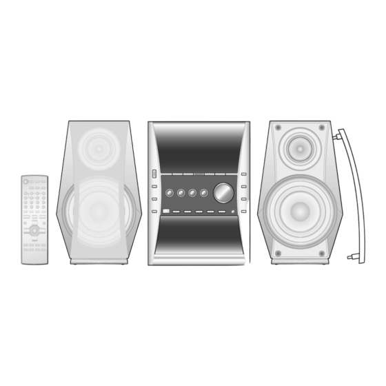
Page 8: Accessories
SA-PM31P / SA-PM31PC 7 Accessories Note : Refer to Packaging Materials & Accessories for the part number. AC power cord FM indoor antenna AM loop antenna Remote control... -
Page 9: Operating Procedures
SA-PM31P / SA-PM31PC 8 Operating Procedures... - Page 10 SA-PM31P / SA-PM31PC...
-
Page 11: Assembling And Disassembling
SA-PM31P / SA-PM31PC 9 Assembling and Disassembling “ATTENTION SERVICER” Some chassis components may be have sharp edges. Be careful when disassembling and servicing. 1. This section describes procedures for checking the operation of the major printed circuit boards and replacing the main components. -
Page 12: Disassembly Of Side Panel L & R
SA-PM31P / SA-PM31PC 9.2. Disassembly of Side Panel L & Step 1 : Remove 1 screw. Step 2 : Lift up the top Cabinet as arrow shown (be careful of the catches). Step 1 : Remove 5 screws. Step 2 : Remove 1 screw. -
Page 13: Disassembly Of Front Panel Assembly
SA-PM31P / SA-PM31PC Step 1 : Detach the connector CN308. Step 1 : Remove 1 screw. Step 2 : Release the clutch. Step 2 : Detach the connector CN505. Step 3 : Remove 4 screws. Step 4 : Push the lever as arrow shown to open the cassette lid and remove the Deck Mechanism Unit. -
Page 14: Disassembly Of Main Control P.c.b., Function P.c.b. And
SA-PM31P / SA-PM31PC Step 2 : Release 2 clutches and remove both Function P.C.B. and Power-In P.C.B. · Disassembly of Main Control P.C.B. Step 3 : Remove 2 screws to remove the shield plate. Step 3 : Release 2 catches and remove the front panel as Step 4 : Remove 2 screws and flip the Main Control P.C.B. -
Page 15: Disassembly Of Rear Panel
SA-PM31P / SA-PM31PC Step 1 : Detach the connector CN303. Step 1 : Remove the volume knob. Step 2 : Remove 9 screws. Step 3: Remove the rear panel as arrows shown (Be careful of the catches). Step 2 : Remove 7 screws. -
Page 16: Disassembly Of Transformer
SA-PM31P / SA-PM31PC Step 1 : Detach the connectors CN505 and CN506. Step 1 : Detach the connectors CN308, CN305 and CN306 . Step 2 : Remove 4 screws and pull out the Transformer P.C.B. as arrow shown. 9.11. Disassembly of Tuner Pack Step 2 : Detach the connectors CN304 (pull the catch as arrow shown), CN301 and CN302 and pull out the Main P.C.B as... -
Page 17: Disassembly Of Power P.c.b
SA-PM31P / SA-PM31PC Step 1 : Detach the connector CN101 and remove the tuner pack as arrow shown. 9.12. Disassembly of Power P.C.B · Follow the (Step 1) - (Step 6) of Item 9.2. · Follow the (Step 1) - (Step 3) of Item 9.3. -
Page 18: Replacement Of Cd Lid
SA-PM31P / SA-PM31PC Step 1 : Remove 2 screws and the 2 CD lid supports. Step 4 : Release the catches and remove the middle block as arrow shown. Step 2 : Push the spring as arrow shown. Step 5 : Remove 2 screws and remove the CD Mechanism Unit from the bottom chassis. -
Page 19: Replacement Of Cassette Lid
SA-PM31P / SA-PM31PC Step 3 : Remove the CD lid as arrow shown. 9.15. Replacement of Cassette Lid · Follow the (Step 1) - (Step 6) of Item 9.2. · Follow the (Step 1) - (Step 3) of Item 9.3. -
Page 20: Replacement Of The Power Ic And Transistors
SA-PM31P / SA-PM31PC 9.16. Replacement of the Power IC and Transistors. · Follow the (Step 1) - (Step 6) of Item 9.2. · Follow the (Step 1) - (Step 3) of Item 9.3. · Follow the (Step 1) - (Step 3) of Item 9.8. -
Page 21: Procedure For Replacing Pinch Roller And Head Block
SA-PM31P / SA-PM31PC 9.17. Procedure for Replacing Pinch Roller and Head Block (Cassette Mechanism Unit) · Follow the (Step 1) - (Step 6) of Item 9.2. · Follow the (Step 1) - (Step 3) of Item 9.3. · Follow the (Step 1) - (Step 4) of Item 9.4. - Page 22 SA-PM31P / SA-PM31PC...
-
Page 23: Procedure For Replacing Parts On Mechanism Pcb
SA-PM31P / SA-PM31PC 9.19. Procedure for Replacing Parts on Mechanism PCB · Follow the (Step 1) - (Step 6) of Item 9.2. · Follow the (Step 1) - (Step 3) of Item 9.3. · Follow the (Step 1) - (Step 4) of Item 9.4. - Page 24 SA-PM31P / SA-PM31PC · Follow the (Step 1) - (Step 3) of Item 9.3. · Follow the (Step 1) - (Step 4) of Item 9.5. · Follow the (Step 1) - (Step 5) of Item 9.13.
-
Page 25: Replacement Of Optical Pickup Unit (Cd Mechanism)
SA-PM31P / SA-PM31PC 9.21. Replacement of optical pickup unit (CD mechanism) · Follow the (Step 1) - (Step 6) of Item 9.2. · Follow the (Step 1) - (Step 3) of Item 9.3. · Follow the (Step 1) - (Step 4) of Item 9.5. -
Page 26: Replacement Of A Traverse Gear A And A Traverse Gear B
SA-PM31P / SA-PM31PC 9.22. Replacement of a traverse gear A and a traverse gear B · Follow the (Step 1) - (Step 6) of Item 9.2. · Follow the (Step 1) - (Step 3) of Item 9.3. · Follow the (Step 1) - (Step 4) of Item 9.5. -
Page 27: Procedure For Removing Cd Loading Mechanism
SA-PM31P / SA-PM31PC · Follow the (Step 1) - (Step 5) of Item 9.13. · Follow the (Step 1) - (Step 2) of Item 9.20. · Follow the (Step 1) - (Step 12) of Item 9.21. 9.23. Procedure for removing CD loading mechanism 1. - Page 28 SA-PM31P / SA-PM31PC 2. Insert the hexgonal wrench (2.5mm) into the gear. 9.24.2. Replacement for the disc tray · Follow the (Step 1) - (Step 6) of Item 9.2. · Follow the (Step 1) - (Step 3) of Item 9.3.
- Page 29 SA-PM31P / SA-PM31PC...
- Page 30 SA-PM31P / SA-PM31PC 9.24.3. Replacement for the traverse deck · Follow the (Step 1) - (Step 6) of Item 9.2. · Follow the (Step 1) - (Step 3) of Item 9.3. · Follow the (Step 1) - (Step 4) of Item 9.5.
- Page 31 SA-PM31P / SA-PM31PC 9.24.4. Disassembly for CD loading unit · Follow the (Step 1) - (Step 6) of Item 9.2. · Follow the (Step 1) - (Step 3) of Item 9.3. · Follow the (Step 1) - (Step 4) of Item 9.5.
- Page 32 SA-PM31P / SA-PM31PC...
- Page 33 SA-PM31P / SA-PM31PC...
-
Page 34: Cr16 Mechanism Assembly Procedure
SA-PM31P / SA-PM31PC 9.25. CR16 MECHANISM ASSEMBLY PROCEDURE The following specified greases and/or oil must be applied when some specific parts are changed. 1. Floil grease (VFK1298) : The floil grease must be applied to tray, tray (L) and tray (R). - Page 35 SA-PM31P / SA-PM31PC...
- Page 36 SA-PM31P / SA-PM31PC...
- Page 37 SA-PM31P / SA-PM31PC...
- Page 38 SA-PM31P / SA-PM31PC...
- Page 39 SA-PM31P / SA-PM31PC...
- Page 40 SA-PM31P / SA-PM31PC...
- Page 41 SA-PM31P / SA-PM31PC...
- Page 42 SA-PM31P / SA-PM31PC...
- Page 43 SA-PM31P / SA-PM31PC...
- Page 44 SA-PM31P / SA-PM31PC...
- Page 45 SA-PM31P / SA-PM31PC...
-
Page 46: Disassembly Of Traverse Mechanism
SA-PM31P / SA-PM31PC 9.26. Disassembly of traverse mechanism · Follow the (Step 1) - (Step 6) of Item 9.2. · Follow the (Step 1) - (Step 3) of Item 9.3. · Follow the (Step 1) - (Step 4) of Item 9.5. -
Page 47: Handling Of Cassette Tape Jam
SA-PM31P / SA-PM31PC Step 1 : If the cassette tape cannot eject due to twinning around capstan or pinch roller during play or record, rotate the flywheel F as arrow shown to remove twined tape. Step 2 : Push the lever as arrow shown to open the cassette lid and remove the cassette tape. -
Page 48: Service Positions
SA-PM31P / SA-PM31PC 10 Service Positions 10.1. Checking procedure Note : For the disassembling procedure, see the section 9. 10.2. Checking the major P.C.B. 1. Disassembly of Side Panel L & R 2. Disassembly of Top Cabinet 3. Disassembly of Deck P.C.B. and Tape Eject P.C.B. -
Page 49: Self-Diagnostic Display Function
SA-PM31P / SA-PM31PC 11 Self-Diagnostic Display Function This unit is equipped with a self-diagnostic display function, which will be useful during servicing and maintenance. · Refer to the next page for display symbols, symptoms, etc. 11.1. Entering into Self-Diagnostic Mode 11.1.1. - Page 50 SA-PM31P / SA-PM31PC d) Power down to exit by pressing [ POWER] button on the main unit. e) The CLEAR key on the remote controller when used in any test items mode shall end the current test, operations and exit Doctor Mode.
-
Page 51: Clearing Self-Diagnostic Memory
SA-PM31P / SA-PM31PC (Note) In the case that you unplug from AC outlet after this mode was set, then plug to AC again, a cold start shall begin. And “- - - - - - - - -” is displayed in the FL for 2 seconds. -
Page 52: Error Code Table
SA-PM31P / SA-PM31PC 11.4. Error Code Table 11.4.1. Error code for Power Supply Error Code Abnormal Items Possible Cause POWER AMP output During normal operation, if either DCDET1 or DCDET2 becomes L, normal POWER OFF abnormal process shall not be executed, PCNT shall be switched to L immediately. GOODBYE shall not display and the error display F61 is displayed instead. -
Page 53: Changer Reliability Test Mode
SA-PM31P / SA-PM31PC Operation Procedures Micon operation & processing [TAPE ] Key is pressed, after loading in a TPS operation is executed. Check the following. NORMAL, CrO2, METAL type cassette ( { F.REC INH SW } is ON cassette for TPS checking purposes and with { R.REC INH SW } is ON... -
Page 54: Cr16 Mechanism Ageing Mode
SA-PM31P / SA-PM31PC 11.8. CR16 Mechanism Ageing Mode To enter into ageing mode: 1. Enter a Doctor mode. 2. Press [2] button on the remote control. It enters into ageing mode (See Fig. 11.8). Ageing process: 1. Tray 1 open. -
Page 55: Procedure For Checking Operation Of Individual Parts Of
SA-PM31P / SA-PM31PC 12 Procedure for Checking Operation of Individual Parts of Cassette Mechanism Unit 12.1. Operation Check with Cassette Tape 1. Pull up the EJECT lever using a rubber band. (Cf. Fig. 6) 2. Supply DC5V to MOTOR. (→ MOTOR rotates.) (Cf. Fig. 5) 3. - Page 56 SA-PM31P / SA-PM31PC Fig. 7...
-
Page 57: Measurement And Adjustments
SA-PM31P / SA-PM31PC 13 Measurement And Adjustments 13.1. Tuner/CD Sections No adjustment required. 13.2. Cassette Deck Section 13.2.1. Requirements · Test tape (QZZCFM) (QZZCWAT) · Normal blank cassette tape (QZZCRA) · Frequency indicator · Oscilloscope · Electrical voltmeter · Headphone jack output jig (Cf. Fig. 8) 13.2.2. - Page 58 SA-PM31P / SA-PM31PC Fig. 10 Fig. 11 13.2.5. Bias Voltage Check 1. Connect an electrical voltmeter. (Cf. Fig. 9) (Cf. Fig. 12) 2. Set the function to “TAPE” position. 3. Insert a normal blank cassette tape (QZZCRA). 4. While pressing and holding down [REC ( )] button, press [TAPE ( )] button to pause the recording mode.
-
Page 59: Voltage Measurement And Waveform Chart
SA-PM31P / SA-PM31PC 14 Voltage Measurement and Waveform Chart CD SERVO P.C.B. IC702 Ref No. MODE CD PLAY STANDBY Ref No. IC702 MODE CD PLAY STANDBY Ref No. IC702 MODE CD PLAY STANDBY Ref No. IC702 MODE CD PLAY STANDBY IC 703 Ref No. - Page 60 SA-PM31P / SA-PM31PC MAIN CONTROL P.C.B. Ref No. IC 600 MODE CD PLAY -30.4 -30.4 -28.0 -28.0 -28.0 -28.0 -28.0 -28.0 -28.0 -28.0 -28.0 -28.0 STANDBY -27.6 -27.6 -26.4 -26.5 -26.5 -26.5 -26.6 -26.6 -26.6 -26.6 -26.7 -26.7 Ref No.
- Page 61 SA-PM31P / SA-PM31PC MAIN P.C.B. Ref No. Q200 Q201 Q222 Q223 Q224 MODE CD PLAY 11.2 10.3 -2.4 STANDBY -2.5 -2.3 -2.0 Ref No. Q301 Q302 Q303 Q304 Q305 MODE CD PLAY STANDBY Q306 Q307 Q308 Q309 Q310 Ref No.
-
Page 62: Waveform
SA-PM31P / SA-PM31PC 14.1. Waveform CN306 PIN 4 CN306 PIN 5 CN306 PIN 6 CN306 PIN 7 CD PLAY CD PLAY CD PLAY CD PLAY 3.84Vp-p (25msec.div) 3.64Vp-p (25msec.div) 4.04Vp-p (25msec.div) 4.48Vp-p (25msec.div) CN306 PIN 8 CN308 PIN 10 CN308 PIN 11... -
Page 63: Block Diagram
SA-PM31P / SA-PM31PC 15 Block Diagram 15.1. CD Servo Block OPTICAL PICKUP SEMICONDUCTOR LASER Q701 LASER POWER DRIVE PHOTO DETECTOR IC703 BA5948FPE2 4CH DRIVE VREF FOCUS LEVEL [CH3] COIL SHIFT TRACKING [CH4] LEVEL COIL SHIFT M701 LEVEL [CH2] TRAVERSE SHIFT... - Page 64 SA-PM31P / SA-PM31PC TO MAIN BLOCK IC702 MN6627953HB SERVO PROCESSOR DIGITAL SIGNAL PROCESSOR/ DIGITAL FILTER/ D/A CONVERTER CD SIGNAL OUTL OUTR BLKCK BLKCK SPOUT SDPOL(PC) TRVP MCLK MCLK MDATA MDATA STAT STAT X701...
-
Page 65: Main Block
SA-PM31P / SA-PM31PC 15.2. Main Block FILTER (DECK 2) R/P HEAD IC1001 AN7326K P/B REC AMP 22(1) 21(2) 20(3) 19(4) 16(7) 15(8) RIPPLE REJECTION LOGIC SWITCH REC AMP (L) MUTE Q1101 (Q1201) IC1000 C1AA00000612 MUTING ANALOG SWITCH SWITCH Q1302 Q1317... - Page 66 SA-PM31P / SA-PM31PC 4(3) 1(2) 5(6) IC300 C1BB00000757 9(10) 17(16) Q725 Q710 (Q726) (Q711) MUTING MUTING SWITCH SWITCH IC501 C0AABB000125 OP AMP Q721 (Q720) D709 (D708) JK600 HEADPHONE JK303 Q201 TUNER PACK REGULATOR Z301 Q223 Q222 Q718 (Q423) (Q422) (Q719)
- Page 67 SA-PM31P / SA-PM31PC FL 600 FROM FL DISPLAY TRANSFORMER RM21 RM11 LOADING MOTOR UP/DOWN MOTOR 40,1,2 22~16 14~11 IC11 IC21 C0GAG0000007 C0GAG0000007 UP/DOWN LOADING IC600 MOTOR MOTOR DRIVER DRIVER C0HBB0000044 DIG00 FL DRIVER IC302 C2CBJG000574 MICROPROCESSOR Q309 Q310 MOTOR SWITCH...
- Page 68 SA-PM31P / SA-PM31PC MOTOR SWITCH Q700~ Q703 Q515,Q516 SWITCH (DCDET) TO CD BLOCK Q306 Q304 Q305 DCDET SWITCH S701 SWITCH SWITCH RESET SWITCH IC302 PCONT C2CBJG000574 MICROPROCESSOR BOTTOM CHANGE PLAY STOCK OPEN PHOTO COUPLER...
- Page 69 SA-PM31P / SA-PM31PC SIGNAL LINES : MAIN SIGNAL LINE : TAPE PLAYBACK SIGNAL LINE : CD-DA SIGNAL LINE : FM/AM SIGNAL LINE : TAPE RECORD SIGNAL LINE : AUX SIGNAL LINE Note : Signal Lines are applicable to the Left Channel only.
-
Page 70: Notes Of Schematic Diagram
SA-PM31P / SA-PM31PC 16 Notes of Schematic Diagram (All schematic diagrams may be modified at any time with Secondary trouble can be prevented by taking care during the development of new technology) repair. · Cover the parts boxes made of plastics with aluminium foil. -
Page 71: Schematic Diagram
SA-PM31P / SA-PM31PC 17 Schematic Diagram 17.1. CD Servo Circuit SCHEMATIC DIAGRAM - 1 CD SERVO CIRCUIT : +B SIGNAL LINE : CD-DA SIGNAL LINE OPTICAL PICKUP UNIT C701 6.3V33 R701 Q701 B1ADCF000001 CN701 LASER POWER DRIVE Vref R754 HUL7213... - Page 72 SA-PM31P / SA-PM31PC SCHEMATIC DIAGRAM - 2 : CD-DA SIGNAL LINE CD SERVO CIRCUIT : +B SIGNAL LINE : CD SIGNAL LINE C703 C704 C755 C724 C723 6.3V100 6.3V220 C727 R717 50V1 C725 1000P C726 C728 R718 R711 1000P 50V1...
-
Page 73: Main Circuit
SA-PM31P / SA-PM31PC 17.2. Main Circuit SCHEMATIC DIAGRAM-3 : FM/AM SIGNAL LINE : MAIN SIGNAL LINE : TAPE PLAYBACK SIGNAL LINE : CD SIGNAL LINE MAIN CIRCUIT : TAPE RECORD SIGNAL LINE : AUX SIGNAL LINE : +B SIGNAL LINE... - Page 74 SA-PM31P / SA-PM31PC SCHEMATIC DIAGRAM-4 : MAIN SIGNAL LINE : FM/AM SIGNAL LINE : TAPE RECORD SIGNAL LINE MAIN CIRCUIT : TAPE PLAYBACK SIGNAL LINE : CD SIGNAL LINE : +B SIGNAL LINE CN308 SSEQ_LED SSEQ_LED SW5V SW5V SYNC SYNC...
- Page 75 SA-PM31P / SA-PM31PC SCHEMATIC DIAGRAM-5 MAIN CIRCUIT : +B SIGNAL LINE C345 100P C344 100P C304 100P R480 R306 R384 4.7K /RST R383 C303 470P R382 PLAY_SW RESTSW /RESTSW PCONT STATUS HP_SW R479 HP_SW DCDET WA114 SSEQ_LED R381 SSEQ_LED RE_LED...
- Page 76 SA-PM31P / SA-PM31PC SCHEMATIC DIAGRAM-6 : MAIN SIGNAL LINE MAIN CIRCUIT : CD SIGNAL LINE : +B SIGNAL LINE CN305 +7.5V +7.5V PGND CHANGESW CR16 SWITCH R326 4.7K DNGD R325 M2_FOUT UP/DOWN F M2_ROUT UP/DOWN R R324 4.7K BT_SW BOTTOM SW...
-
Page 77: Main Control Circuit, Panel Circuit, Power-In Circuit And
SA-PM31P / SA-PM31PC 17.3. Main Control Circuit, Panel Circuit, Power-In Circuit and Function Circuit SCHEMATIC DIAGRAM-7 MAIN CONTROL CIRCUIT : +B SIGNAL LINE C600 50V22 PANEL CIRCUIT Z601 VR600 EVEJ1CF3024B B3RAB0000040 VOLUME JOG REMOTE CONTROL SENSOR R629 C610 C608 1000P 6.3V47... - Page 78 SA-PM31P / SA-PM31PC SCHEMATIC DIAGRAM-8 : +B SIGNAL LINE MAIN CONTROL CIRCUIT : +B SIGNAL LINE FL600 A2BB00000131 FL DISPLAY 2 3 4 5 6 7 8 9 10 11 12 13 14 15 16 17 18 19 20 21 22 23 24 25 26 27 28 29 30 31 32 33 34 35 36 37 38 39 40 41 42 43 44...
-
Page 79: Deck Circuit, Deck Mechanism Circuit And Tape Eject Circuit
SA-PM31P / SA-PM31PC 17.4. Deck Circuit, Deck Mechanism Circuit and Tape Eject Circuit SCHEMATIC DIAGRAM-9 : TAPE PLAYBACK SIGNAL LINE DECK CIRCUIT : TAPE RECORD SIGNAL LINE : +B SIGNAL LINE C1105 470P R1103 C1122 0.01 R1101 C1104 0.027 C1102... -
Page 80: Circuit
SA-PM31P / SA-PM31PC SCHEMATIC DIAGRAM-10 : TAPE PLAYBACK SIGNAL LINE DECK CIRCUIT : TAPE RECORD SIGNAL LINE : +B SIGNAL LINE Q1101,Q1201 B1ABGC000005 MUTTING SWITCH R1105 R1109 2.2K R1107 Q1101 C1110 R1106 6800P 100K R1209 R1205 2.2K R1207 Q1201 R1206... -
Page 81: Power Circuit
SA-PM31P / SA-PM31PC 17.5. Power Circuit SCHEMATIC DIAGRAM-11 : -B SIGNAL LINE POWER CIRCUIT : +B SIGNAL LINE : MAIN SIGNAL LINE R778 D708 R776 MA2C16500E C738 R774 16V10 100K R772 4.7K Q720 KTC3199GRTA R758 R752 2.2K 100K C750 0.01... - Page 82 SA-PM31P / SA-PM31PC SCHEMATIC DIAGRAM-12 : -B SIGNAL LINE POWER CIRCUIT : +B SIGNAL LINE : MAIN SIGNAL LINE Q701 R704 Q703 KTA12710YTA B1AACF000063 SWITCH SWITCH Q700 C700 R702 R707 6.3V100 5.6K R705 C701 16V33 R710 C703 R711 C704 820K D706 6.3V220...
- Page 83 SA-PM31P / SA-PM31PC SCHEMATIC DIAGRAM-13 : -B SIGNAL LINE POWER CIRCUIT : +B SIGNAL LINE : MAIN SIGNAL LINE IC500 RSN315H41-P POWER AMP IC C515 0.01 CN504 R514 HI_R C503 820P RGND C509 R506 R763 RGND C501 820P R761 5.6K...
-
Page 84: Transformer Circuit
SA-PM31P / SA-PM31PC 17.6. Transformer Circuit SCHEMATIC DIAGRAM-14 : -B SIGNAL LINE TRANSFORMER CIRCUIT : +B SIGNAL LINE Q578 KRC102MTA SWITCH D578 D581 R580 R581 R585 Q575 B0EAKM000117 B0EAKM000117 B1AAGC000006 ECONOMY SWITCH C585 C584 Q577 25V100 16V1000 2SC3940ARA REGULATOR R583... -
Page 85: Cd Loading Circuit
SA-PM31P / SA-PM31PC 17.7. CD Loading Circuit SCHEMATIC DIAGRAM-15 CD LOADING CIRCUIT : +B SIGNAL LINE IC11 C0GAG0000007 UP/DOWN MOTOR DRIVE 0.01 16V100 RM11 UP/DOWN MOTOR CHANGE BOTTOM OPEN B3NAA0000068 SENSOR +7.5V STOCK PGND CR16 SWITCH DNGD UP/DOWN F PLAY... -
Page 86: Printed Circuit Board
SA-PM31P / SA-PM31PC 18 Printed Circuit Board 18.1. CD Servo P.C.B. CD SERVO P.C.B (REPV0039A) C755 TP51 C727 C718 TP19 C725 C726 TP16 R711 J711 TP23 TP50 C716 J722 C728 TP17 C702 TP18 C705 TP87 C729 C706 TP13 TP27 C762... -
Page 87: Main P.c.b
SA-PM31P / SA-PM31PC 18.2. Main P.C.B. MAIN P.C.B (REPV0037A) PHONES L602 L601 C604 W216 W236 R453 WA101 W278 R357 W206 R358 IC303 C325 W400 W221 Q301 W305 W205 C306 W421 CN308 W422 W409 R336 R320 W472 R327 R319 C345 R338... - Page 88 SA-PM31P / SA-PM31PC PHONES W236 WA101 W400 W221 C306 W421 C381 R336 W472 C345 R337 W451 R450 W272 W413 W331 W415 W276 W296 W293 W295 CN101 (TO TUNER PACK Z301) W277 W420 W340 R456 W339 W281 R349 W280 Q305 W334...
-
Page 89: Main Control P.c.b. And Panel P.c.b
SA-PM31P / SA-PM31PC 18.3. Main Control P.C.B. and Panel P.C.B. MAIN CONTROL P.C.B (REPV0037A) C620 FL600 C600 9 10 11 12 13 14 15 16 17 18 19 20 21 22 23 24 25 26 27 28 29 30 31 32... -
Page 90: Power In P.c.b., Function P.c.b. And Deck Mechanism P.c.b
SA-PM31P / SA-PM31PC 18.4. Power In P.C.B., Function P.C.B. and Deck Mechanism P.C.B. POWER IN P.C.B (REPV0037A) H601B/JW601 S617 S616 R636 D609 CD CHECK S615 SURROUND S614 POWER FUNCTION P.C.B (REPV0037A) S620 S623 S621 S622 CD CHANGE DECK MECHANISM P.C.B (REPX0321H) -
Page 91: Deck P.c.b. And Tape Eject P.c.b
SA-PM31P / SA-PM31PC 18.5. Deck P.C.B. and Tape Eject P.C.B. DECK P.C.B (REPV0016B) WR1308B W1930 CN1305 Q1309 Q1310 R1380 W1909 W1935 C1317 R1331 W1977 C1311 Q1303 L1301 W1947 Q1312 R1327 W1946 Q1304 C1314 D1301 L1302 R1335 R1337 Q1302 W1942 C1310... -
Page 92: Cd Loading
SA-PM31P / SA-PM31PC 18.6. CD Loading P.C.B. CD LOADING P.C.B (REP3569A) BOTTOMSW RM11 IC11 UPDOWN PLAYSW CHANGESW STOCKSW RM21 LOADING_MOTOR IC21 OPENSW... -
Page 93: Power P.c.b
SA-PM31P / SA-PM31PC 18.7. Power P.C.B. POWER P.C.B (REPV0038A) PM31...W518 CN504 IC500 W770 C503 C515 R505 D515 R524 R518 C504 C500 C502 R506 D520 R520 R519 C501 R515 C505 Q509 C510 R511 R532 W763 C521 R545 R514 R760 R542 W764... -
Page 94: Transformer P.c.b
SA-PM31P / SA-PM31PC 18.8. Transformer P.C.B. TRANSFORMER P.C.B (REPV0038A) 125V 2A W509 Q577 R583 R584 W505 W513 CN505 W514 C581 RL501 T501 (MAIN TRANSFORMER) W549 C585 W531 R595 C578 H503/ Q575 FP501 D584 JW503 R578 C575 Q578 C582 Q579 L503... -
Page 95: Wiring Connection Diagram
SA-PM31P / SA-PM31PC 19 Wiring Connection Diagram H603B/JW603 CD SERVO P.C.B 9 ..1 CN702 PANEL P.C.B CN701 M701 TRV MOTOR 16 15 SOLDER SIDE M702 SPL MOTOR SOLDER SIDE SOLDER SIDE MAIN CONTROL P.C.B... - Page 96 SA-PM31P / SA-PM31PC PHONE CN303 MAIN P.C.B JK600 CN308 CN101 1..10 JK303 21... 1 20 ..2 CN309 2.
-
Page 97: Illustration Of Ic 痴, Transistors And Diodes
SA-PM31P / SA-PM31PC 20 Illustration of IC’s, Transistors and Diodes CNB13030R2AU (4P) C0AABB000125 (8P) C1BB00000757 (24P) C0HBB0000044 (40P) C1AA00000612 (5P) BA5948FPE2 (28P) MN6627953HB (80P) AN7326K (22P) C2CBJG000574 (100P) KRA102MTA RSN315H41-P (18P) C0DBZGC00067 C0GAG0000007 (9P) 2SB0621AHA KRC102MTA KRA110MTA B1ACCF000063 KTC3199GRTA 2SD0592ARA... -
Page 98: Terminal Function Of IcエS
SA-PM31P / SA-PM31PC 21 Terminal Function of IC´s 21.1. IC702 (MN6627953HB) Servo Pin No. Mark Function RFOUT RF Amp output processor/ Digital signal RFIN AGC input processor/ Digital filter/ D/A CAGC AGC control terminal ARFOUT AGC output (Audio RF) converter... -
Page 99: Ic302 (C2Cbjg000574) Micro Processor
SA-PM31P / SA-PM31PC Pin No. Mark I/O Function Pin No. Mark I/O Function PGND1 Ground Connection (1) for Driver Motor Driver (4) reverse - action output PVCC1 Power Supply (1) for Driver Motor Driver (4) forward - action Motor Driver (1) reverse - action... - Page 100 SA-PM31P / SA-PM31PC Pin No. Mark Function RE_LED MP3/WMA Re-master Control MOTOR MOTOR Control Output L=OFF, H=ON PLUNGER Deck PLUNGER Control Output L=OFF, H=ON DECK_AD1 DECK AD Input 1 DECK_AD2 DECK AD Input 2 REG1 Region Setting 1 KEY3 KEY3 INPUT...
-
Page 101: Troubleshooting Flowchart (Cd Section Circuit)
SA-PM31P / SA-PM31PC 22 Troubleshooting Flowchart (CD Section Circuit) - Page 102 SA-PM31P / SA-PM31PC...
-
Page 103: Parts Location And Replacement Parts List
SA-PM31P / SA-PM31PC 23 Parts Location and Replacement Parts List Notes: · Important safety notice: Components identified by mark have special characteristics important for safety. Furthermore, special parts which have purposes of fire-retardant (resistors), high-quality sound (capacitors), low noise (resistors), etc are used. -
Page 104: Deck Mechanism
SA-PM31P / SA-PM31PC 23.1. Deck Mechanism 23.1.1. Deck Mechanism Parts Location (RAA4402-S) -
Page 105: Deck Mechanism Parts List
SA-PM31P / SA-PM31PC 23.1.2. Deck Mechanism Parts List Ref. Part No. Part Name & Description Remarks CASSETTE DECK RED0067 R/P HEAD BLOCK UNIT RDG0300 REEL BASE GEAR RDG0301 WINDING RELAY GEAR RDK0026 MAIN GEAR RDV0033-4 WINDING BELT RDV0064 CAPSTAN BELT... -
Page 106: Cd Loading Mechanism
SA-PM31P / SA-PM31PC 23.2. CD Loading Mechanism 23.2.1. CD Loading Mechanism Parts Location... - Page 107 SA-PM31P / SA-PM31PC...
- Page 108 SA-PM31P / SA-PM31PC...
- Page 109 SA-PM31P / SA-PM31PC...
-
Page 110: Cd Loading Mechanism Parts List
SA-PM31P / SA-PM31PC 23.2.2. CD Loading Mechanism Parts List Ref. Part No. Part Name & Description Remarks RMR1407E-H6 TRAY 5 Ref. Part No. Part Name & Description Remarks RFKNAPM77MDS MECHA BASE ASS’Y RMR1427-X MIDDLE CHASSIS TRAVERSE DECK RMS0757-1 FIXED PIN... -
Page 111: Cabinet
SA-PM31P / SA-PM31PC 23.3. Cabinet 23.3.1. Cabinet Parts Location... - Page 112 SA-PM31P / SA-PM31PC...
- Page 113 SA-PM31P / SA-PM31PC...
-
Page 114: Electrical Part List
SA-PM31P / SA-PM31PC 23.3.2. Cabinet Parts List Ref. Part No. Part Name & Description Remarks RKF0688-S CASS HOLDER/LID Ref. Part No. Part Name & Description Remarks RKMV0045-S TOP CABINET RKMV0046-S SIDE PANEL LEFT CABINET AND CHASSIS RKMV0047-S SIDE PANEL RIGHT... - Page 115 SA-PM31P / SA-PM31PC Ref. Part No. Part Name & Description Remarks Ref. Part No. Part Name & Description Remarks Q715 KTC3199GRTA TRANSISTOR VR600 EVEJ1CF3024B VOL. ENCORDER Q716 KTC3199GRTA TRANSISTOR Q717 KTC3199GRTA TRANSISTOR SWITCHES Q718 B1AAGC000006 TRANSISTOR Q719 B1AAGC000006 TRANSISTOR K0L1BA000065...
- Page 116 SA-PM31P / SA-PM31PC Ref. Part No. Part Name & Description Remarks Ref. Part No. Part Name & Description Remarks L600 J0JBC0000019 CHIP INDUCTOR WA106 ERJ3GEY0R00V CHIP JUMPER L601 J0JBC0000019 CHIP INDUCTOR WA107 ERJ3GEY0R00V CHIP JUMPER L602 G0C100JA0030 INDUCTOR WA108 ERJ3GEY0R00V...
- Page 117 SA-PM31P / SA-PM31PC Ref. Part No. Part Name & Description Remarks Ref. Part No. Part Name & Description Remarks R328 D0GB101JA007 100 1/16W R450 ERJ3GEYJ102V 1K 1/16W R329 ERJ3GEYJ102V 1K 1/16W R452 D0GB101JA007 100 1/16W R330 D0GB474JA041 470K 1/16W R453...
- Page 118 SA-PM31P / SA-PM31PC Ref. Part No. Part Name & Description Remarks Ref. Part No. Part Name & Description Remarks R591 D0AE101JA048 100 1/4W R727 ERJ3GEYJ102V 1K 1/16W R595 ERDS1FVJ1R0T 1 1/2W R728 D0AE102JA048 1K 1/4W R600 ERJ3GEYJ680V 68 1/16W R728...
- Page 119 SA-PM31P / SA-PM31PC Ref. Part No. Part Name & Description Remarks Ref. Part No. Part Name & Description Remarks R798 D0AE102JA048 1K 1/4W C212 F1H1H102A219 1000P 50V R799 D0AE102JA048 1K 1/4W C214 F1H1H2210001 220P 50V R972 ERDS2TJ821T 820 1/4W C217...
- Page 120 SA-PM31P / SA-PM31PC Ref. Part No. Part Name & Description Remarks Ref. Part No. Part Name & Description Remarks C417 ECJ1VC1H102J 1000P 50V C622 F1H1H2210001 220P 50V C419 ECA1CAK100XB 10 16V C700 ECA0JAK101XB 100 6.3V C420 ECA1CAK100XB 10 16V C701...
- Page 121 SA-PM31P / SA-PM31PC Ref. Part No. Part Name & Description Remarks C744 F1H1E1530002 0.015 25V C745 F1D1H101A012 100P 50V C745 F1H1E103A029 0.01 25V C746 F1D1H101A012 100P 50V C746 F1H1C104A041 0.1 16V C747 F1D1H270A006 27P 50V C747 F1H1H391A013 390P 50V C748...
-
Page 122: Packaging Materials & Accessories Parts List
SA-PM31P / SA-PM31PC 23.5. Packaging Materials & Accessories Parts List Ref. Part No. Part Name & Description Remarks Ref. Part No. Part Name & Description Remarks PACKING MATERIALS N2QAJB000132 REMOTE CONTROL A1-1 RKK-HTR0051K R/C BATTERY COVER RPGV0175 PACKING CASE [M]P...