Table of Contents
Advertisement
HIGH POWER CD/MP3/WMA PLAYER WITH BLUETOOTH WIRE-
LESS TECHNOLOGY, RDS TUNER AND MULTI-CD CONTROL
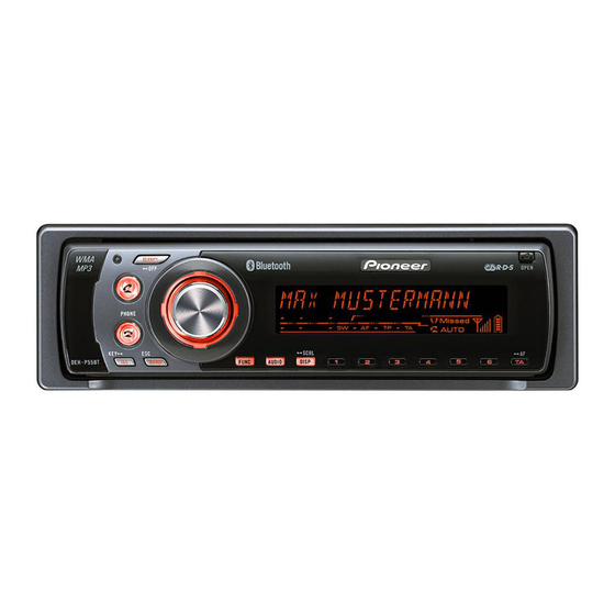
DEH-P55BT
This service manual should be used together with the following manual(s):
Model No.
Order No.
CX-3164
CRT3583
For details, refer to "Important Check Points for Good Servicing".
PIONEER CORPORATION
PIONEER ELECTRONICS (USA) INC. P.O. Box 1760, Long Beach, CA 90801-1760, U.S.A.
PIONEER EUROPE NV Haven 1087, Keetberglaan 1, 9120 Melsele, Belgium
PIONEER ELECTRONICS ASIACENTRE PTE. LTD. 253 Alexandra Road, #04-01, Singapore 159936
PIONEER CORPORATION 2006
Mech.Module
S10.5COMP1
CD Mech. Module : Circuit Descriptions, Mech. Descriptions, Disassembly
4-1, Meguro 1-chome, Meguro-ku, Tokyo 153-8654, Japan
DEH-P55BT/XN/EW
Remarks
ORDER NO.
CRT3598
/XN/EW5
K-ZZW. JAN. 2006 Printed in Japan
Advertisement
Table of Contents

Related Manuals for Pioneer DEH-P55BT/XN/EW5


Summary of Contents for Pioneer DEH-P55BT/XN/EW5
- Page 1 PIONEER CORPORATION 4-1, Meguro 1-chome, Meguro-ku, Tokyo 153-8654, Japan PIONEER ELECTRONICS (USA) INC. P.O. Box 1760, Long Beach, CA 90801-1760, U.S.A. PIONEER EUROPE NV Haven 1087, Keetberglaan 1, 9120 Melsele, Belgium PIONEER ELECTRONICS ASIACENTRE PTE. LTD. 253 Alexandra Road, #04-01, Singapore 159936 PIONEER CORPORATION 2006 K-ZZW.
-
Page 2: Safety Information
ICs inside the unit. 3. To protect the pickup unit from electrostatic discharge during servicing, take an appropriate treatment (shorting-solder) by referring to "the DISASSEMBLY". 4. After replacing the pickup unit, be sure to check the grating. DEH-P55BT/XN/EW5... - Page 3 To protect products from damages or failures during transit, the shipping mode should be set or the shipping screws should be installed before shipment. Please be sure to follow this method especially if it is specified in this manual. DEH-P55BT/XN/EW5...
-
Page 4: Table Of Contents
7. GENERAL INFORMATION ..........................66 7.1 DIAGNOSIS ............................. 66 7.1.1 DISASSEMBLY ............................. 66 7.1.2 CONNECTOR FUNCTION DESCRIPTION ..................71 7.2 PARTS..............................72 7.2.1 IC ................................72 7.2.2 DISPLAY ............................... 85 7.3 OPERATIONAL FLOW CHART ....................... 86 8. OPERATIONS ..............................87 DEH-P55BT/XN/EW5... -
Page 5: Specifications
1. SPECIFICATIONS DEH-P55BT/XN/EW5... - Page 6 DEH-P55BT/XN/EW5...
- Page 7 DEH-P55BT/XN/EW5...
-
Page 8: Exploded Views And Parts List
• Screw adjacent to mark on the product are used for disassembly. • For the applying amount of lubricants or glue, follow the instructions in this manual. (In the case of no amount instructions,apply as you think it appropriate.) 2.1 PACKING DEH-P55BT/XN/EW5... - Page 9 24-8 Polyethylene Bag E36-634 Polyethylene Bag CEG-162 Case Assy CXB3520 Sub Carton CHG5195 Carton CHG5879 Owner's Manual,Installation Manual Part No. Language CRD4062 English, Spanish CRD4063 German, French CRD4064 Italian, Dutch CRB2140 Russian CRD4065 English, Spanish, German, French, Italian, Dutch, Russian DEH-P55BT/XN/EW5...
-
Page 10: Exterior
2.2 EXTERIOR DEH-P55BT/XN/EW5... - Page 11 106 Spring CBL1512 IC(IC351) PAL007B 107 Pin CNV6486 108 Holder Unit CXC5760 IC(IC911) NJM2388F84 109 CD Mechanism Module(S10.5) CXK5752 Transistor(Q551,751) 2SD2396 110 Screw ISS26P055FTC Choke Coil(L981) CTH1280 Detach Grille Assy CXC5586 111 Insulator XNM7106 Screw BPZ20P100FTB Button(SRC) CAC9520 Button(ILL,BAND) CAC9521 DEH-P55BT/XN/EW5...
-
Page 12: Cd Mechanism Module
2.3 CD MECHANISM MODULE DEH-P55BT/XN/EW5... - Page 13 Bracket CND2583 CND2584 Lever CND2585 CND2586 Bracket CND2587 CND2588 Lever CND2589 Holder CNV7201 Gear CNV7207 Gear CNV7208 Gear CNV7209 Gear CNV7210 Gear CNV7211 Gear CNV7212 Rack CNV7214 CNV7216 Roller CNV7218 Gear CNV7219 Guide CNV7361 Gear CNV7595 Guide CNV7799 CNV7805 DEH-P55BT/XN/EW5...
-
Page 14: Block Diagram And Schematic Diagram
CD CONTROLLER MECHA VD Q751 B.UP ROT0 12EJ Q752 ROT1 X701 4.00MHz DSCSNS VDCONT VDCONT HOME VDCONT S904 S905 S901 12EJ HOME CD3VON SWVDD S802 S903 DSCSNS CSENS DSENS D SENSE SW DPDT/TSO IC203 V3R3D NJM2886DL3-33 KYDT/TSI +3.3V REGULATOR DEH-P55BT/XN/EW5... - Page 15 DISP ON HOOK ROT1 ROT1 ROT1 SWVDD KDT1-4,KST1 KDT1-4 SWVDD Q831 SWVDD REM.CON. SWVDD (ILLUMINATION) TSOP4840SB1 SWVDD Q832 CSENS CSENS KST1 KEY DATA POUT1 LED DRIVE DPDT DPDT DPDT/TSO LCD DRIVER/ 5.00MHz KYDT KYDT KEY CONTROLLER KYDT/TSI PD6538A LCD1 DEH-P55BT/XN/EW5...
-
Page 16: Overall Connection Diagram(Guide Page)
Note: When ordering service parts, be sure to refer to " EXPLODED VIEWS AND PARTS LIST" or "ELECTRICAL PARTS LIST". Large size SCH diagram WIRED REMOTE CONTROL Guide page Detailed page CD:+0.3dBs FM(30%):-20.0dBs AM(30%):-20.0dBs SYSTEM CONTROL CN10 8.1V EJECT IB-BUS:+2.2dBs PANEL UNIT DEH-P55BT/XN/EW5... - Page 17 No differentiation is made between chip capacitors and ← 0.022 R022 discrete capacitors. The > mark found on some component parts indicates the importance of the safety factor of the part. Therefore, when replacing, be sure to use parts of identical designation. DEH-P55BT/XN/EW5...
- Page 18 DEH-P55BT/XN/EW5...
- Page 19 DEH-P55BT/XN/EW5...
- Page 20 DEH-P55BT/XN/EW5...
- Page 21 DEH-P55BT/XN/EW5...
-
Page 22: Keyboard Unit
3.3 KEYBOARD UNIT CN1951 VOLUME LCD DRIVER DEH-P55BT/XN/EW5... - Page 23 KEYBOARD UNIT : The power supply is shown with the marked box. DEH-P55BT/XN/EW5...
-
Page 24: Cd Mechanism Module(Guide Page)
3.4 CD MECHANISM MODULE(GUIDE PAGE) PICKUP UNIT(P10.5)(SERVICE) SWITCHES: CD CORE UNIT(S10.5COMP1) S901:HOME SWITCH..ON-OFF S903:DSCSNS SWITCH..ON-OFF S904:12EJ SWITCH.....ON-OFF S905:8EJ SWITCH....ON-OFF The underlined indicates the switch position. CD DRIVER M1 CXC6742 SPINDLE MOTOR M2 CXC4026 LOADING/CARRIAGE MOTOR DEH-P55BT/XN/EW5... - Page 25 SIGNAL LINE FOCUS SERVO LINE TRACKING SERVO LINE CARRIAGE SERVO LINE SPINDLE SERVO LINE CD CORE UNIT(S10.5COMP1) + 3.3 V REGULATOR CD3VON(MCKRQ) SRAMLEVEL2 ADENA SRAMLEVEL1 SRAMLEVEL0 (S904) CD CONTROLLER (S905) CN701 DEH-P55BT/XN/EW5...
- Page 26 DEH-P55BT/XN/EW5...
- Page 27 DEH-P55BT/XN/EW5...
- Page 28 DEH-P55BT/XN/EW5...
- Page 29 DEH-P55BT/XN/EW5...
- Page 30 200 mV/div 500 mV/div ! TE 500 mV/div 8 TIN 500 mV/div CD-ROM play operation(Regular track Jump) Spindle waveform during play operation Spindle waveform during play operation (Wider) Ref.: Ref.: Ref.: REFO REFO REFO Mode: Mode: Mode: Normal Normal Normal DEH-P55BT/XN/EW5...
- Page 31 500 mV/div 4 LOEJ 3 12SNS 8 TIN 5 V/div 5 V/div 500 mV/div CD-DA → CD-ROM mode change(Band key) 12 cm CD Eject operation 8 cm CD Eject operation Ref.: Ref.: Ref.: REFO Mode: Mode: Mode: Normal Normal Normal DEH-P55BT/XN/EW5...
- Page 32 7 CIN 8 TIN 500 mV/div 1 V/div 8 TIN ! TE 500 mV/div 1 V/div 9 FIN 1 V/div CD-ROM → CD-DA mode change(Band key) Black dot(800 µm) during play Ref.: Ref.: REFO REFO Mode: Mode: Normal Normal DEH-P55BT/XN/EW5...
- Page 33 DEH-P55BT/XN/EW5...
-
Page 34: Bluetooth Unit
3.5 BLUETOOTH UNIT BLUETOOTH PCB ANTENNA PCB DEH-P55BT/XN/EW5... - Page 35 BLUETOOTH UNIT Consists of BLUETOOTH PCB ANTENNA PCB DEH-P55BT/XN/EW5...
-
Page 36: Pcb Connection Diagram
For further information for respective destinations, be sure to check with the schematic dia- CORD ASSY gram. 2.Viewpoint of PCB diagrams IP-BUS Capacitor Connector SIDE A SIDE B P.C.Board Chip Part TUNER AMP UNIT CORD ASSY CN1051 DSENSE RESE DEH-P55BT/XN/EW5... - Page 37 SIDE A SUB WOOFER OR FRONT OUTOUT REAR OUTPUT FM/AM ANTENNA RESET CN901 CN1950 FRONT DEH-P55BT/XN/EW5...
- Page 38 TUNER AMP UNIT DEH-P55BT/XN/EW5...
- Page 39 SIDE B DEH-P55BT/XN/EW5...
-
Page 40: Keyboard Unit
4.2 KEYBOARD UNIT KEYBOARD UNIT SIDE A DEH-P55BT/XN/EW5... - Page 41 KEYBOARD UNIT SIDE B CN1951 DEH-P55BT/XN/EW5...
-
Page 42: Cd Core Unit(S10.5Comp1)
4.3 CD CORE UNIT(S10.5COMP1) SIDE A CD CORE UNIT(S10.5COMP1) PICKUP UNIT(P10.5)(SERVICE) CN701 REFO1 HOME CN901 LOADING /CARRIAGE MOTOR SPINDLE MOTOR IC203 IC301 DEH-P55BT/XN/EW5... - Page 43 SIDE B CD CORE UNIT(S10.5COMP1) 12EJ DSCSNS DEH-P55BT/XN/EW5...
-
Page 44: Bluetooth Pcb
4.4 BLUETOOTH PCB BLUETOOTH PCB SIDE A DEH-P55BT/XN/EW5... - Page 45 BLUETOOTH PCB SIDE B BT MODULE ANT1102 DEH-P55BT/XN/EW5...
-
Page 46: Panel Unit
4.5 PANEL UNIT PANEL UNIT SIDE A CN10 EJECT SIDE B PANEL UNIT CN801 DEH-P55BT/XN/EW5... -
Page 47: Antenna Pcb
4.6 ANTENNA PCB SIDE B ANTENNA PCB SIDE A ANTENNA PCB ANT1001 BT ANTENNA DEH-P55BT/XN/EW5... -
Page 48: Electrical Parts List
Q 301 (A,141,127) Transistor IMH3A D 805 (B,111,29) Diode DAP202U D 806 (B,110,23) Diode DAN202U Q 303 (A,157,127) Transistor IMH3A D 807 (B,96,19) Diode UMZ6R8EN Q 304 (A,155,119) Transistor UMD2N D 821 (A,18,27) Diode HZS9L(B1) Q 351 (B,119,136) Transistor DTC114EU DEH-P55BT/XN/EW5... - Page 49 R 211 (A,105,106) RAB4C102J R 552 (B,20,82) RS1/16S223J R 212 (B,68,89) RS1/16S103J R 553 (A,14,85) RD1/4PU332J R 213 (B,67,81) RS1/16S103J R 556 (A,14,93) RD1/4PU0R0J R 214 (B,70,89) RS1/16S103J R 581 (A,40,69) RS1/16S105J R 215 (B,68,81) RS1/16S103J R 582 (B,36,71) RS1/16S332J DEH-P55BT/XN/EW5...
- Page 50 C 233 (A,65,81) CKSRYB104K16 R 820 (B,111,35) RS1/16S222J C 234 (A,67,81) CKSRYB104K16 R 821 (A,17,32) RD1/4PU182J C 241 (B,74,89) CCSRCH470J50 R 824 (B,44,14) RS1/16S222J C 242 (B,72,81) CCSRCH470J50 R 831 (B,69,25) RS1/16S472J C 243 (A,64,85) CKSRYB104K16 R 832 (B,64,25) RS1/16S102J DEH-P55BT/XN/EW5...
- Page 51 S 10 (A,151,7) Push Switch CSG1155 C 803 (B,105,21) CCSRCH220J50 S 11 (A,66,7) Push Switch CSG1155 C 820 (A,43,12) CEJQ1R0M50 S 12 (A,56,7) Push Switch CSG1155 C 821 (A,18,24) CKSRYB104K16 S 13 (A,18,26) Push Switch CSG1155 C 822 (B,51,11) CKSRYB224K16 DEH-P55BT/XN/EW5...
- Page 52 R 56 (B,145,5) RS1/16S222J C 28 (B,116,37) CKSQYB225K10 R 57 (B,144,13) RS1/16S101J C 29 (A,24,12) CKSRYB104K16 R 58 (B,151,9) RS1/16S820J C 30 (A,24,10) CKSRYB104K16 R 59 (B,151,6) RS1/16S121J C 82 (A,14,38) CKSRYF104Z50 R 60 (B,136,4) RS1/16S102J C 83 (B,126,13) CKSRYB103K50 DEH-P55BT/XN/EW5...
- Page 53 R 1010 (A,28,26) RS1/16S334J S 903 (B,23,78) Switch(DSCSNS) CSN1067 R 1021 (B,25,42) RS1/16S203J S 904 (B,42,87) Switch(12EJ) CSN1068 R 1022 (B,25,40) RS1/16S203J S 905 (B,28,88) Switch(8EJ) CSN1068 R 1023 (B,29,41) RS1/16S103J R 1024 (B,29,40) RS1/16S103J RESISTORS R 1031 (B,11,39) RS1/16S393J DEH-P55BT/XN/EW5...
- Page 54 (B,20,32) RS1/16SS0R0J CAPACITORS C 103 (B,57,83) CEVW101M16 C 108 (A,47,66) CKSSYB104K10 C 201 (B,46,56) CKSSYB102K50 C 202 (B,47,58) CKSSYB104K10 C 204 (B,35,48) CEVW220M6R3 C 205 (A,34,63) CKSSYB104K10 C 208 (B,34,54) CKSSYB104K10 C 209 (B,31,57) CKSSYB104K10 C 210 (A,31,66) CKSRYB105K10 DEH-P55BT/XN/EW5...
-
Page 55: Adjustment
1k ohms in series. • The load and eject operation is not guarantied with the mechanism upside down. If the mechanism is blocked due to mistaken eject operation, reset the product or turn off and on the ACC to restore it. DEH-P55BT/XN/EW5... - Page 56 • When the power is turned on/off the jump mode is reset to the Single TR (91) while the gain of the RFAMP is reset to 0 dB. At the same time all the self-adjusting values shall return to the default setting. DEH-P55BT/XN/EW5...
-
Page 57: Checking The Grating After Changing The Pickup Unit
Because of eccentricity in the disc and a slight misalignment of the clamping center the grating waveform may be seen to "wobble" ( the phase difference changes as the disc rotates). The angle specified above indicates the average angle. • Hint Reloading the disc changes the clamp position and may decrease the "wobble". DEH-P55BT/XN/EW5... - Page 58 Ech → Xch 20mV/div, AC Grating waveform Fch → Ych 20mV/div, AC 0° 30° 45° 60° 75° 90° DEH-P55BT/XN/EW5...
-
Page 59: Error Mode
Remarks: Mechanical errors are not displayed (because a CD is turned off in these errors). Unreadable TOC does not constitute an error. An intended operation continues in this case. Upper digits of an error code are subdivided as shown below: 1x: Setup relevant errors, 3x: Search relevant errors, Ax: Other errors. DEH-P55BT/XN/EW5... -
Page 60: Bluetooth Test Mode
This enables user to avoid the task of registering phones and transfering phone directory again even after resetting system at the time of battery exchange, etc. • Registration of phone • Phone directory • History of sending/arrival • Dial preset DEH-P55BT/XN/EW5... - Page 61 You can use a BT-supporting mobile phone to check BT operation in a simple method. The following three points shall be checked in the test mode: • Bluetooth Connection (authentication connection and voice connection) Check • BT Antenna Sensitivity (Connection) Check • FLASH Memory Operation Check 3. Configuration Scheme DEH-P55BT Bluetooth DEH-P55BT/XN/EW5...
- Page 62 The numeric value serves only as a guide. If you place a mobile phone in front of the product, the display shows about 30 – 60. If you get a different value or no display at all, BT antenna connection is not good. DEH-P55BT/XN/EW5...
- Page 63 Module and connect to ANT connector inside Bluetooth unit A: U.FL-SMA conversion adapter (Hirose Electric Co., Ltd CL311-0301-5) B: Coaxial cable for SMA microwave (Stack Electronics Co., Ltd. P-100-STF358) • C: SMA conversion connector (Stack Electronics Co., Ltd. BA057) DEH-P55BT/XN/EW5...
- Page 64 “BT-TEST” is shown for 3 seconds. *2 : After display of “BT-TEST”, the screen changes automatically. HSP is abbreviation of HEAD_SET_ PROFILE. *3 : In measurement, each of 02, 41, and 80 is measured. Go back to SEL Screen using the BAND key. DEH-P55BT/XN/EW5...
-
Page 65: System Microcomputer Test Program
The frequency of the clock signal is 468.75kHz that is one 32th of the fundamental frequency. The clock signal should be 468.75kHz ± 19Hz. If the clock signal is out of the range, the X'tal (X601) should be replaced with new one. DEH-P55BT/XN/EW5... -
Page 66: General Information
Remove the four screws. Disconnect the connector and then remove the CD Mechanism Module. Fig.1 Removing the Grille Assy (Fig.2) Disconnect the Cord Assy by Jig GGF1539. Remove the two screws and then remove the Grille Assy. Grille Assy Cord Assy Fig.2 DEH-P55BT/XN/EW5... - Page 67 Do not insert the cord assy in extreme slant, as the connector might suffer damage. Removing the Tuner Amp Unit (Fig.4) Remove the screw. Remove the three screws. Straighten the tabs at three locations indicated. Remove the screw and then remove the Tuner Amp Unit. Tuner Amp Unit Fig.4 DEH-P55BT/XN/EW5...
- Page 68 Removing the Bluetooth Unit (Fig.5) Remove the solder. Remove the solder. Straighten the three tabs, and then remove the Bluetooth Unit. Bluetooth Unit Fig.5 DEH-P55BT/XN/EW5...
- Page 69 Upper Frame. 3. While lifting the Carriage Mechanism, remove it from the three Dampers. Caution: When assembling, be sure to apply some alcohol to the Dampers and assemble the mechanism in a clamped state. Damper Damper Carriage Mechanism Lower Frame DEH-P55BT/XN/EW5...
- Page 70 Assemble the sub unit side of the Pickup, taking the plate (Chassis) in-between. When treating the leads of the Load Carriage Motor Assy, do not make them loose over the Feed Screw. Poly Washer Change Arm Pickup Lock Arm Inner Holder Feed Screw Planet Gear Pickup Rack Chassis Pickup DEH-P55BT/XN/EW5...
-
Page 71: Connector Function Description
4. RR- 12. NC 6. GND 5. FL+ 13. NC 7. BUS L+ INPUT 6. RL+ 14. ACC 8. ASENB 7. FL- 15. GND 9. BUS R+ INPUT 8. RL- 16. BACKUP 10. BUS R- INPUT 11. BUS L- INPUT DEH-P55BT/XN/EW5... -
Page 72: Parts
12 4A 2A 4 11 4Y 2B 5 10 3B 2Y 6 9 3A GND 7 8 3Y NJM2388F84 Bandgap Reference 1 2 3 4 ON/OFF Cont control Over Voltage Thermal Over Current Protection Protection Protection 3.GND 4.ON/OFF CONTROL DEH-P55BT/XN/EW5... - Page 73 Stand-by P-GND2 Circuit OUT2- Offset Protector; STBY Detection Thermal OUT2+ OUT1- Offset P-GND1 Detection OUT1+ Protector; S-GND Short circuit AC-GND OUT3+ Offset P-GND3 Detection OUT3- OUT4+ Offset MUTE Detection OUT4- P-GND4 SWITCH Protector; Over current limit Mute circuit DEH-P55BT/XN/EW5...
- Page 74 PML015A - Block Diagram - Pin Layout IN1_R IN1_L IN2_R IN2_L IN3_R IN3_L IN4+_R IN4+_L IN4-_R IN4-_L Front_R Front_L Rear_R Rear_L Vref DATA FIE_R FIE_L Pre/SW_R Pre/SW_L LMout PGND Pref DEH-P55BT/XN/EW5...
- Page 75 S99-50084 AN6123MS INPUT GND OUTPUT :Serial clock input :Serial data input HOLD# :Serial data output :Chip select input HOLD :Hold input :Supply voltage input :Ground HA12241FP -BUS +BUS BIAS DRIVER OUTPUT (current) RECEIVER OUTPUT R out DEH-P55BT/XN/EW5...
- Page 76 MEMWP External memory : Write protect output RGBCK RGB DAC IC : Clock input RGBST RGB DAC IC : Strobe output RGBDT RGB DAC IC : Data output RECIVE Not used CSENSOUT CSENS output TUNPDI TUNER : PLL communication DEH-P55BT/XN/EW5...
- Page 77 AD translation power supply input terminal TUNER : Signal level input VREF AD translation reference voltage AVCC AD translation power supply input terminal MEMDI External memory : Data input MEMDO External memory : Data output MEMCK External memory : Clock output * PEG238A DEH-P55BT/XN/EW5...
- Page 78 19 18 17 16 15 14 13 9 10 11 12 -Block Diagram VFTN VFTP AMPT BCLK PCM I/F AMPR CODEC Core Internal Main Clock PLLC TAGND MUTEN VREF BGREF RSTN AMP1 AMP2 TEST1 TEST2 TEST3 AMP1O AMP1I AMP2O AMP2I DEH-P55BT/XN/EW5...
- Page 79 Connect to GND RESET Reset input Crystal oscillator connection pin Crystal oscillator connection pin Remote control reception input 58,59 ROUT2,3 Not used 60-63 KDT4-1 Key data input 64-69 KST6-1 Key strobe output 70-100 SEG69-39 LCD segment output * PD6538A BU2507FV DEH-P55BT/XN/EW5...
- Page 80 VDCONT VD power supply control output CD LSI serial data input CD LSI serial data output CD LSI serial clock output xwait CD LSI wait control signal input CD LSI address strobe output XASTB Address/data Bus 0 Not used DEH-P55BT/XN/EW5...
- Page 81 Not used Not used 91-93 csens Not used Not used TYPE_A/D Not used 96,97 TEMP Not used VD power supply short sense input VDSENS DSCSNS Not used * PE5505A Format meaning C MOS NJM2886DL3-33 Thermal Protection Bandgap Reference CONTROL DEH-P55BT/XN/EW5...
- Page 82 Ground for 1.6 V digital circuits D1.GND Output of 33.8688 MHz(CLK for SDRAM) C33M DRAM cs (rcs) Output of DRAM address 11 RA11 (CKE) Output of DRAM CKE Output of DRAM ras Output of DRAM lower cas(LDQM) cas)(LDQM) Output of DRAM upper cas(UDQM) cas!(UDQM) DEH-P55BT/XN/EW5...
- Page 83 Connected to the capacitor for output of REFOUT Reversal input of FE Output of FE Input of FE, TE A/D converter ADIN Reversal input of TE Output of TE Output of LD Input of PD Ground for digital circuits D.GND * UPD63763CGJ DEH-P55BT/XN/EW5...
- Page 84 22 AUDIOGND audio ground Ground of audio block 23 L ch O L channel output FM stereo “L-ch” signal output or AM audio output 24 R ch O R channel output FM stereo “R-ch” signal output or AM audio output DEH-P55BT/XN/EW5...
-
Page 85: Display
7.2.2 DISPLAY - LCD (CAW1926) DEH-P55BT/XN/EW5... -
Page 86: Operational Flow Chart
In case of the above signal, the communication with Grille microcomputer may fail. Source keys If the time interval is not 300msec, the oscillator operative may be defective. Source ON SYSPW←H Pin 1 Completes power-on operation. (After that, proceed to each source operation) DEH-P55BT/XN/EW5... -
Page 87: Operations
8. OPERATIONS DEH-P55BT/XN/EW5... - Page 88 DEH-P55BT/XN/EW5...
- Page 89 DEH-P55BT/XN/EW5...
- Page 90 DEH-P55BT/XN/EW5...
- Page 91 1. Attach the holders to both sides of the front panel. Holder Holder CND2699 CND1250 2. Replace the front panel to the unit. 3. Flip the holders into upright positions. 4. Fix the front panel to the unit using fixing screws. Fixing Screw BPZ20P060FTB DEH-P55BT/XN/EW5...
- Page 92 - CONNECTION DIAGRAM DEH-P55BT/XN/EW5...
- Page 93 DEH-P55BT/XN/EW5...
- Page 94 CD Mechanism Module Before shipping out the product, be sure to clean the following portions by using the prescribed cleaning tools: Portions to be cleaned Cleaning tools CD pickup lenses Cleaning liquid : GEM1004 Cleaning paper : GED-008 g p p DEH-P55BT/XN/EW5...