JVC KS-AX3300 Schematic Diagrams
Hide thumbs
Also See for KS-AX3300:
- User manual ,
- Service manual (27 pages) ,
- Instructions manual (6 pages)
Advertisement
Quick Links
SCHEMATIC DIAGRAMS
Contents
Block diagram
Standard schematic diagram
POWER AMPLIFIER
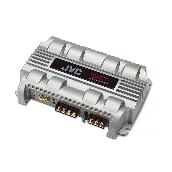
KS-AX3300
CD-ROM No.SML200503
COPYRIGHT
2005 Victor Company of Japan, Limited.
Area suffix
J ---------- Northern America
E ---------- Southern Europe
U ----------------- Other Areas
2-1
2-3
2-5
No.MA171SCH
2005/3
Advertisement

Related Manuals for JVC KS-AX3300


Summary of Contents for JVC KS-AX3300
-
Page 1: Power Amplifier
SCHEMATIC DIAGRAMS POWER AMPLIFIER KS-AX3300 CD-ROM No.SML200503 Area suffix J ---------- Northern America E ---------- Southern Europe U ----------------- Other Areas Contents Block diagram Standard schematic diagram Printed circuit board No.MA171SCH COPYRIGHT 2005 Victor Company of Japan, Limited. 2005/3... - Page 2 Safety precaution Burrs formed during molding may be left over on some parts of the chassis. Therefore, pay attention to such burrs in the case of preforming repair of this system.
- Page 3 < M E M O >...
- Page 4 Block diagram L+,L- SW301 HIGH R+,R- CN901 LPF ON/OFF INPUT IC301 IC302 CN902 INPUT L+,L- R+,R- F901 T901 BATT CN903 LED901 REMOTE IC901...
- Page 5 LEVEL SPEAKER CN904 IC302 IC303 OUTPUT...
- Page 6 Standard schematic diagram...
-
Page 8: Printed Circuit Board
Printed circuit board Main board... - Page 9 < M E M O >...
- Page 10 Victor Company of Japan, Limited AV & MULTIMEDIA COMPANY CAR ELECTRONICS CATEGORY 10-1,1chome,Ohwatari-machi,Maebashi-city,371-8543,Japan Printed in Japan (No.MA171SCH)