Table of Contents
Advertisement
• SERVICING PRECAUTIONS ..................................................................................................................... 1-2
• ESD PRECAUTIONS .................................................................................................................................. 1-4
• SPECIFICATIONS ...................................................................................................................................... 1-5
• ADJUSTMENTS .......................................................................................................................................... 2-1
• TROUBLESHOOTING ................................................................................................................................ 2-3
• WAVEFORMS OF MAJOR CHECK POINT ............................................................................................... 2-8
• BLOCK DIAGRAM ...................................................................................................................................... 2-9
• SCHEMATIC DIAGRAMS ......................................................................................................................... 2-11
• WIRING DIAGRAM ..................................................................................................................................... 2-19
• PRINTED CIRCUIT DIAGRAMS ............................................................................................................... 2-21
• INTERNAL BLOCK DIAGRAM OF ICs ..................................................................................................... 2-30
• CABINET AND MAIN FRAME SECTION .................................................................................................. 3-1
• TAPE DECK MECHANISM: AUTO STOP DECK(OPTIONAL) ................................................................... 3-3
• TAPE DECK MECHANISM: AUTO REVERSE DECK ................................................................................. 3-5
• CD MECHANISM ......................................................................................................................................... 3-7
SECTION 4. SPEAKER .................................................................................................................. 4-1
SECTION 5. REPLACEMENT PARTS LIST .................................................................................. 5-1
CONTENTS
- 1-1 -
Advertisement
Table of Contents

Related Manuals for LG FFH-185A


Summary of Contents for LG FFH-185A
-
Page 1: Table Of Contents
CONTENTS SECTION 1. GENERAL • SERVICING PRECAUTIONS ........................1-2 • ESD PRECAUTIONS ..........................1-4 • SPECIFICATIONS ............................1-5 SECTION 2. ELECTRICAL • ADJUSTMENTS ............................2-1 • TROUBLESHOOTING ..........................2-3 • WAVEFORMS OF MAJOR CHECK POINT ....................2-8 • BLOCK DIAGRAM ............................2-9 •... -
Page 2: Section 1. General
SECTION 1. GENERAL SERVICING PRECAUTIONS NOTES REGARDING HANDLING OF THE PICK-UP 1. Notes for transport and storage 1) The pick-up should always be left in its conductive bag until immediately prior to use. 2) The pick-up should never be subjected to external pressure or impact. Storage in conductive bag Drop impact 2. - Page 3 NOTES REGARDING COMPACT DISC PLAYER REPAIRS 1. Preparations 1) Compact disc players incorporate a great many ICs as well as the pick-up (laser diode). These components are sensitive to, and easily affected by, static electricity. If such static electricity is high voltage, components can be damaged, and for that reason components should be handled with care.
-
Page 4: Esd Precautions
ESD PRECAUTIONS Electrostatically Sensitive Devices (ESD) Some semiconductor (solid state) devices can be damaged easily by static electricity. Such components commonly are called Electrostatically Sensitive Devices (ESD). Examples of typical ESD devices are integrated circuits and some field-effect transistors and semiconductor chip components. The following techniques should be used to help reduce the incidence of component damage caused by static electricity. -
Page 5: Specifications
SPECIFICATIONS 1. AMP SECTION 1) Power Output (6 Ω, 2 channel, T.H.D. 10%) ................20W+20W 2) T.H.D ............................0.15% 3) Frequency Response (-3dB down) ..................42Hz~25kHz 4) Signal-to-noise Ratio ........................80dB 5) Input Sensitivity AUX ......................400±50mV 6) Channel Difference 1kHz ......................... 2dB 2. - Page 6 3. TAPE DECK SECTION 1) Tape Speed (MTT-111) / Normal Speed ................. 4.75cm/sec 2) Wow Flutter (MTT-111) ......................... 0.25% 3) Fast Forward and Rewind Time (C-60) ..................120sec 4) Frequency Response (6dB range) ..................250Hz~8kHz 5) Signal-to-noise Ratio (Playback/Record) ................43dB/43dB 6) Distortion (Playback/Record) ......................
-
Page 7: Section 2. Electrical
SECTION 2. ELECTRICAL ADJUSTMENTS This set has been aligned at the factory and normally will not require further adjustment. As a result, it is not recommended that any attempt is made to modificate any circuit. If any parts are replaced or if anyone tampers with the adjustment, realignment may be necessary. - Page 8 3. TUNER ADJUSTMENT (FM) Item Test Point Adjustment Adjust for DC Voltage Check Point TP1, TP2 L101 0V±50mV Electronic FM Antenna OSCILLOSCOPE Terminal Speaker Signal Generator Unit Figure 3. Tuner(S curve) Adjustment Connection Diagram - 2-2 -...
-
Page 9: Troubleshooting
TROUBLESHOOTING Turn power on. Check power supply circuit. Is power on? (Check PN 501) Does initial read work? Check laser circuit. Check focus circuit. Check disc. Does it play? Check tracking servo circuit. Does it output audio? Check audio circuit. - 2-3 -... - Page 10 Fails to initial read Does laser light? Disc motor turns. Does tracking Does signal Does TE2 signal Does RF servo work? appear at Test appear at pin waveform Defective IC Lower envelope Pin(TEO)? of IC501? appear? 801, pick up of Test Pin(RF) Test Pin(RF) and/or open waveform is flat.
- Page 11 Laser does not light. Is “3.5V” applied to pin of IC 501? Did pickup return to Is data transferred from Defective MICOM. innermost circular? MICOM IC ? Does voltage appear at IC 502 pin Defective IC 501, 502 Defective slide motor and/or connector.
- Page 12 Laser lights. Does IC 501 out focus search signal? Does lens move up/down? Defective IC501 IC 501 pin (FEO) Is focus search signal applied to pin Defective IC502 PN502? Open activator and/or connector. Confirm Does Test Pin RF signal appear even in initial low level? read with...
- Page 13 Does FE1 signal appear? IC 501 Defective IC 501. Open pick diode Does FZC signal (focus zero cross signal) appear at pin of IC 501, ISTAT (SENSE) (Focus servo turns terminal? ON by FZC signal Defective IC 501. of FOK mod.) ISTAT(SENSE) Does SMON signal appear at pin...
-
Page 14: Waveforms Of Major Check Point
WAVEFORMS OF MAJOR CHECK POINT 1. HF signal (RF signal ) waveform 2. EFM signal (pin IC 501)waveform (Test Point) during normal play during Normal Play 0.5V/Div. 2V/Div. 500nS/Div. 500nS/Div. 3. Focus coil drive waveform(Pin NO 1, 2 of IC 502) •... -
Page 15: Block Diagram
BLOCK DIAGRAM NOTE: NOTE: Warning Parts that are shaded are critical With respect 1. Shaded(I) parts are critical for safety.Replace only to risk of fire or electrical shock. with specified part number. 2. Voltages are DC-measured with a digital voltmefer during Play mode. -
Page 16: Schematic Diagrams
SCHEMATIC DIAGRAMS • MAIN SCHEMATIC DIAGRAM NOTE: Warning NOTE: Parts that are shaded are critical With respect 1. Shaded(I) parts are critical for safety.Replace only to risk of fire or electrical shock. with specified part number. 2. Voltages are DC-measured with a digital voltmefer during Play mode. - Page 17 • FRONT/POWER SCHEMATIC DIAGRAM 2-13 2-14...
- Page 18 • TUNER SCHEMATIC DIAGRAM 2-15 2-16...
- Page 19 • CDP SCHEMATIC DIAGRAM 2-17 2-18...
-
Page 20: Wiring Diagram
WIRING DIAGRAM NOTE: Warning Parts that are shaded are critical With respect to risk of fire or electrical shock. 2-19 2-20... -
Page 21: Printed Circuit Diagrams
PRINTED CIRCUIT DIAGRAMS • MAIN/TUNER P.C. BOARD(SOLDER SIDE) 2-21 2-22... - Page 22 • MAIN/TUNER P.C. BOARD(COMPONENT SIDE) 2-23 2-24...
- Page 23 • FRONT/POWER P.C. BOARD(SOLDER SIDE) NOTE: Warning Parts that are shaded are critical With respect to risk of fire or electrical shock. 2-25 2-26...
- Page 24 • FRONT/POWER P.C. BOARD(COMPONENT SIDE) NOTE: Warning Parts that are shaded are critical With respect to risk of fire or electrical shock. 2-27 2-28...
- Page 25 • CD MAIN P.C. BOARD • LED P.C. BOARD - 2-29 -...
-
Page 26: Internal Block Diagram Of Ics
INTERNAL BLOCK DIAGRAM OF ICs I LA1837 I BA3126N REC SW GND P/B SW CONT P/B SW REC SW I KIA6225P/S - 2-30 -... - Page 27 I KIA7805 P/PI ~ KIA7815 P/PI I BU1923(FOR RDS/RBDS) - 2-31 -...
- Page 28 I BU2090F Block diagram Control circuit DATA 12-bit shift register CLOCK Latch Output buffer (open drain) PIN DESCRIPTION Pin No. Pin name Function BU2090/F/FS BU2092/F BU2092/FV DATA Serial data input CLOCK Data shift clock input Data latch clock input parallel data output parallel data output parallel data output parallel data output...
- Page 29 I TDA7265 1000µF 1µF MUTE/ ST-BY IN (L) OUT (L) 1µF 4.7Ω RL (L) IN- (L) 100nF 560Ω µP 560Ω IN- (R) 1µF OUT (R) IN (R) 4.7Ω RL (R) 100nF 1000µF D94AU085 I BA3308 - 2-33 -...
- Page 30 I LC72131, 72131M REFERENCE PHASE DETECTOR DIVIDER CHARGE PUMP XOUT SWALLOW COUNTER UNLOCK FMIN AOUT 1/16. 1/17 4bits DETECTOR 12bits PROGRAMMABLE AMIN DIVIDER DATA SHIFT REGISTER UNIVERSAL IFIN LATCH COUNTER POWER RESET I TDA7440D MUXOUTL TREBLE(L) BIN(L) BOUT(L) L-IN1 100K L-IN2 100K SPKR ATT...
-
Page 31: Section 3. Exploded Views
SECTION 3. EXPLODED VIEWS NOTE) Refer to “SECTION 5 REPLACEMENT PARTS LIST” in order to look for the • CABINET AND MAIN FRAME SECTION part number of each part. -
Page 32: Tape Deck Mechanism: Auto Stop Deck(Optional)
• TAPE DECK MECHANISM: AUTO STOP DECK(OPTIONAL) LOCA. NO PART NO. SPECIFICATION 6730R-F001A CFL4410 PIGEON L-SINGLE A/STOP 6768R-UP01C 50-093-4527 PIGEON UNIT CFL441 6768R-BP01L 02-084-4201 PIGEON BELT/FELT C 6768R-AP01D 50-239-4027 PIGEON ARM CWL44 6768R-AP01E 50-239-4026 PIGEON ARM CWL44 6768R-SP01E 01-082-4654 PIGEON SPRING CWL4 6768R-QP01D 50-093-4328 PIGEON MOTOR(ASSY) 6768R-GP01A... -
Page 33: Tape Deck Mechanism: Auto Reverse Deck
• TAPE DECK MECHANISM: AUTO REVERSE DECK LOCA. NO PART NO. SPECIFICATION 6730R-F001B CRL4428 PIGEON L-SINGLE A/REVERSE 6768R-UP01B 50-093-4329 PIGEON UNIT CRL442 6768R-BP01K 02-084-4200 PIGEON BELT/FELT C 6768R-AP01D 50-239-4027 PIGEON ARM CWL44 6768R-AP01E 50-239-4026 PIGEON ARM CWL44 6768R-SP01E 01-082-4654 PIGEON SPRING CWL4 6768R-QP01D 50-093-4328 PIGEON MOTOR(ASSY) 6768R-GP01A... -
Page 34: Cd Mechanism
• CD MECHANISM LOCA. NO PART NO. SPECIFICATION 4405RCD001A CDM-X233 HZ SHIN HEUNG CDP 4980SC0001A CLAMP ASSY (CDM-X211) 318-317A DISC ASSY 3041RB0004A TOTAL PU (CDM-X209) 3041RB0003A PU(CDM-X209) 6717RCA001A KSM-213VSCM SONY FRONT LOADING 524-012AAAA CLAMP MAGNET (030X018X5T) 384-064B FELT 0.5T,BK 221-527AAAA MAGNET (SECC 0.8T) 327-013AAAA DISC (DURACON M90-44,BK) -
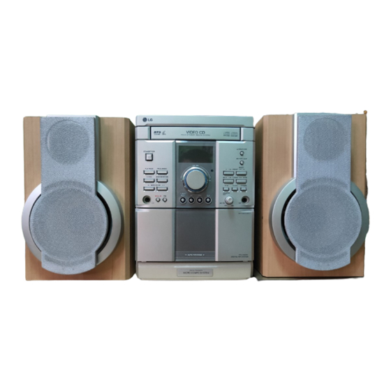
Page 35: Section 4. Speaker
SECTION 4. SPEAKER SECTION MODEL: FE-1850E RUN DATE : 10.MARCH.2003 LOCA.NO. PART NO DESCRIPTION SPECIFICATION REMARK 3701RM0010B NET ASSEMBLY JERSEY NET ASSY FE-185E/DV25VE 4930RM0006A HOLDER RUBBER HOLDER NET (FE-185E/DV2 3720RMF007A PANEL,FRONT FRONT (FE-185E) 6400RMBZ01B SPEAKER,TWEETER B13TP6B2 BALHAE 25VE HZ-LOCAL 6400RMTG01A SPEAKER,WOOFER FE-DV55VE TOPTONE F50C-D138A 6 4766RM0007A... - Page 36 MEMO - 4-2 -...