Table of Contents
Advertisement
Quick Links
TABLE OF CONTENTS
1 Safety Precaution ------------------------------------------------ 2
1.1. General guidelines ---------------------------------------- 2
1.2. Caution for fuse replacement--------------------------- 2
2 Warning -------------------------------------------------------------- 3
2.1. Prevention of Electrostatic Discharge (ESD)
to Electrostatic Sensitive (ES) Devices -------------- 3
2.2. Service caution based on legal restrictions --------- 4
3 Specifications ----------------------------------------------------- 5
4 Service Mode ------------------------------------------------------ 6
4.1. Self-Diagnosis and Special Mode Setting ----------- 6
5 Service Fixture & Tools----------------------------------------14
6 Measurements and Adjustments---------------------------15
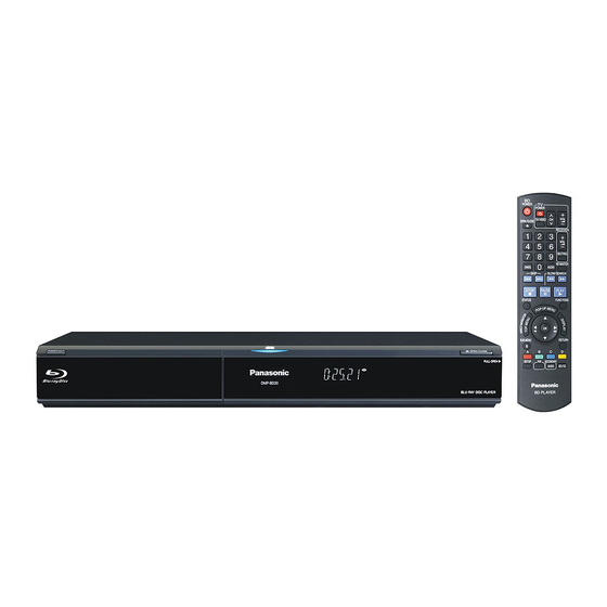
DMP-BD30PP
Model No.
DMP-BD30PL
Vol. 2
Colour
(K).......................Black Type
PAGE
6.1. Service Positions----------------------------------------- 15
© 2007 Matsushita Electric Industrial Co., Ltd. All
rights reserved. Unauthorized copying and distribu-
tion is a violation of law.
ORDER NO.DSD0711018CE
Blu-ray Disc Player
B35
PAGE
Advertisement
Table of Contents

Related Manuals for Panasonic DMP-BD30PP


Summary of Contents for Panasonic DMP-BD30PP
- Page 1 ORDER NO.DSD0711018CE Blu-ray Disc Player DMP-BD30PP Model No. DMP-BD30PL Vol. 2 Colour (K).......Black Type TABLE OF CONTENTS PAGE PAGE 1 Safety Precaution ------------------------------------------------ 2 6.1. Service Positions----------------------------------------- 15 1.1. General guidelines ---------------------------------------- 2 1.2. Caution for fuse replacement--------------------------- 2 2 Warning -------------------------------------------------------------- 3 2.1.
- Page 2 1 Safety Precaution 1.1. General guidelines 1. When servicing, observe the original lead dress. If a short circuit is found, replace all parts which have been overheated or damaged by the short circuit. 2. After servicing, see to it that all the protective devices such as insulation barriers, insulation papers shields are properly installed.
- Page 3 2 Warning 2.1. Prevention of Electrostatic Discharge (ESD) to Electrostatic Sensitive (ES) Devices Some semiconductor (solid state) devices can be damaged easily by static electricity. Such components commonly are called Elec- trostatic Sensitive (ES) Devices. Examples of typical ES devices are integrated circuits and some field-effect transistor-sand semi- conductor chip components.
- Page 4 2.2. Service caution based on legal restrictions 2.2.1. General description about Lead Free Solder (PbF) The lead free solder has been used in the mounting process of all electrical components on the printed circuit boards used for this equipment in considering the globally environmental conservation. The normal solder is the alloy of tin (Sn) and lead (Pb).
- Page 5 3 Specifications...
- Page 6 4 Service Mode 4.1. Self-Diagnosis and Special Mode Setting 4.1.1. Self-Diagnosis Functions Self-Diagnosis Function provides information for errors to service personnel by Self-Diagnosis Display when any error has occurred. U**, H** and F** are stored in memory and held. You can check latest error code by transmitting [0] [1] of Remote Controller in Service Mode. Automatic Display on FL will be cancelled when the power is turned off or AC input is turned off during self-diagnosis display is ON.
- Page 7 Error Code Diagnosis contents Description Monitor Display Automatic FL display UNSUP- Unsupported disc error *An unsupported format disc was played, This disc PORT although the drive starts normally. incompatible. *The data format is not supported, although the media type is supported. *Exceptionally in case of the disc is dirty.
- Page 8 Item FL display Key operation Mode name Description Front Key Forced power-off When the power button is not effective while Display in P-off mode. Press [POWER] key over than 10 power is ON, turn off the power forcibly. seconds. Aging Perform sequence of modes as * Aging Display following the then mode.
- Page 9 Item FL display Key operation Mode name Description Front Key Demonstration lock/ Ejection of the disc is prohibited. *When lock the tray. When the power is on (SS mode), unlock The lock setting is effective until unlocking the press [SKIP FWD] and [OPEN/ tray released Main...
- Page 10 4.1.3. Service Modes at a glance Service mode setting: While the power is off, press [SKIP FWD], [PAUSE] and [OPEN / CLOSE] simultaneously for five seconds. Item FL display Key operation Mode name Description (Remote controller key) Release Items Item of Service Mode executing is cancelled. Press [0] [0] or [Return] in service mode.
- Page 11 Item FL display Key operation Mode name Description (Remote controller key) BD/DVD drive last error BD/DVD drive error code display. 1. Error Number is displayed for 5 Press [4] [2] in service mode. seconds. 2. Time when the error has occurred is display for 5 seconds.
- Page 12 Item FL display Key operation Mode name Description (Remote controller key) In case that the maker cannot be 6. Disc maker ID is displayed for 5 identified, display is black out. seconds. 7. Factor of drive error (hexadeci- mal) occurring is left displayed.
- Page 13 Item FL display Key operation Mode name Description (Remote controller key) CEC (H) output Check of the CEC terminal high output of Press [5] [5] in service mode. HDMI. CEC (L) output Check of the CEC terminal low output of Press [5] [6] in service mode.
- Page 14 5 Service Fixture & Tools Part Number Description Compatibility RFKZ0216 Extension Cable (AV Out P.C.B. - Digital P.C.B./ 23 Pin) Same as EH55 Series Extension Cable (Power P.C.B. - Digital P.C.B. / 23 Pin) RFKZ0366 Extension FFC (BD/DVD Drive - Digital P.C.B. / 40 Pin) Same as EH55 Series RFKZ0169 Extension Cable (Power P.C.B.
- Page 15 6 Measurements and Adjustments 6.1. Service Positions Note: For description of the disassembling procedure, see the section 9 (vol.1). 6.1.1. Checking and Repairing of Digital P.C.B.
-
Page 16: Table Of Contents
"Standard-Playback" mode when there is no specify mode is mentioned. Model No. DMP-BD30PP 4.Although the voltage and waveform available on here is measured with standard frame, it may be differ from actual measurement due to modification of circuit and so on. -
Page 17: S2. Voltage And Waveform Chart
S2. Voltage and Waveform Chart Note) Indicated voltage values are the standard values for the unit measured by the DC electronic circuit tester (high-impedance) with the chassis taken as standard. Therefore, there may exist some errors in the voltage values, depending on the internal impedance of the DC circuit tester. S2.1. -
Page 18: S3. Block Diagram
(DC/DC CONVERTER) IC51001 OUT1 (D+1.2V) OUT2 15 EXT-U P1102 P58007 X SW+5.8V X SW+5.8V P58002 P3001 AV OUT P.C.B. IC58301 (REG.HDMI+5V) JK56001 V IN VOUT (HDMI+5V) DMP-BD30PP/PL Digital P.C.B. Regulator Block Diagram P1102 P58007 X SW+12V P58003 P4001 AV OUT P.C.B. -
Page 19: S3.2. Digital Block Diagram
VOUT8 ED0-15_B HOST I/F Boot IC51303 (8Mbit EEPROM) DDR I/F DDR I/F DDR SDRAM DDR SDRAM DDR SDRAM DDR SDRAM DDR SDRAM DDR SDRAM 512Mbit 512Mbit 512Mbit 512Mbit 512Mbit 512Mbit DMP-BD30PP/PL Digital Block Diagram IC52003 IC52010 IC52002 IC52001 IC52272 IC52271... -
Page 20: S3.3. Ic Pin Terminal Chart
A5(3N) C0A10 AM14 C0A10 A10(2H) C1A6 C1A6 A6(7N) C0A11 AJ17 C0A11 A11(7K) C1A7 C1A7 A7(2P) C0A12 AN16 C0A12 A12(2L) C1A8 C1A8 A8(8P) C1A9 C1A9 A9(3P) C1A10 C1A10 A10(2M) DMP-BD30PP/PL C1A11 C1A11 A11(7P) IC Pin Terminal Chart (1/2) C1A12 C1A12 A12(2R) -
Page 21: S3.3.2. Ic Pin Terminal Chart (2
EA11 EA12_B AL32 EA12 EA13_B AJ31 EA13 EA14_B AG28 EA14 EA15_B AM34 EA15 AH30 EA16_B EA16 AL33 EA17_B EA17 EA18_B AG29 EA18 EA19_B AK32 EA19 EA20_B AH31 EA20 EA21_B AJ32 EA21 AG30 EA22_B EA22 DMP-BD30PP/PL IC Pin Terminal Chart (2/2) -
Page 23: S4. Schematic Diagram
S4. Schematic Diagram S4.1. Interconnection Diagram DMP-BD30PP/PL Interconnection Diagram... - Page 24 DMP-BD30PP/PL Interconnection Diagram...
- Page 25 DMP-BD30PP/PL Interconnection Diagram S-10...
- Page 26 DMP-BD30PP/PL Interconnection Diagram S-11...
-
Page 27: S4.2. Digital_Net (Dn) Schematic Diagram
S4.2. Digital_Net (DN) Schematic Diagram DMP-BD30PP/PL Digital_Net Section (Digital P.C.B. (1/9)) Schematic Diagram (DN) S-12 S-12... - Page 28 DMP-BD30PP/PL Digital_Net Section (Digital P.C.B. (1/9)) Schematic Diagram (DN) S-13 S-13...
- Page 29 DMP-BD30PP/PL Digital_Net Section (Digital P.C.B. (1/9)) Schematic Diagram (DN) S-14...
- Page 30 DMP-BD30PP/PL Digital_Net Section (Digital P.C.B. (1/9)) Schematic Diagram (DN) S-15...
-
Page 31: S4.3. Dac_Hdmi (Dh) Schematic Diagram
S4.3. DAC_HDMI (DH) Schematic Diagram DMP-BD30PP/PL DAC_HDMI Section (Digital P.C.B. (2/9)) Schematic Diagram (DH) S-16 S-16... - Page 32 DMP-BD30PP/PL DAC_HDMI Section (Digital P.C.B. (2/9)) Schematic Diagram (DH) S-17...
- Page 33 DMP-BD30PP/PL DAC_HDMI Section (Digital P.C.B. (2/9)) Schematic Diagram (DH) S-18...
- Page 34 DMP-BD30PP/PL DAC_HDMI Section (Digital P.C.B. (2/9)) Schematic Diagram (DH) S-19...
-
Page 35: S4.4. Audio_Io (Ai) Schematic Diagram
S4.4. Audio_IO (AI) Schematic Diagram DMP-BD30PP/PL Audio_IO Section (Digital P.C.B. (3/9)) Schematic Diagram (AI) S-20... - Page 36 DMP-BD30PP/PL Audio_IO Section (Digital P.C.B. (3/9)) Schematic Diagram (AI) S-21 S-21...
- Page 37 DMP-BD30PP/PL Audio_IO Section (Digital P.C.B. (3/9)) Schematic Diagram (AI) S-22...
- Page 38 DMP-BD30PP/PL Audio_IO Section (Digital P.C.B. (3/9)) Schematic Diagram (AI) S-23...
-
Page 39: S4.5. Peaks_Pro2 (Pk) Schematic Diagram
S4.5. PEAKS_PRO2 (PK) Schematic Diagram DMP-BD30PP/PL PEAKS_PRO2 Section (Digital P.C.B. (4/9)) Schematic Diagram (PK) S-24... - Page 40 DMP-BD30PP/PL PEAKS_PRO2 Section (Digital P.C.B. (4/9)) Schematic Diagram (PK) S-25...
- Page 41 DMP-BD30PP/PL PEAKS_PRO2 Section (Digital P.C.B. (4/9)) Schematic Diagram (PK) S-26...
- Page 42 DMP-BD30PP/PL PEAKS_PRO2 Section (Digital P.C.B. (4/9)) Schematic Diagram (PK) S-27...
-
Page 43: S4.6. Pro2_Peri (Pe) Schematic Diagram
S4.6. PRO2_PERI (PE) Schematic Diagram DMP-BD30PP/PL PRO2_PERI Section (Digital P.C.B. (5/9)) Schematic Diagram (PE) S-28 S-28... - Page 44 DMP-BD30PP/PL PRO2_PERI Section (Digital P.C.B. (5/9)) Schematic Diagram (PE) S-29 S-29...
- Page 45 DMP-BD30PP/PL PRO2_PERI Section (Digital P.C.B. (5/9)) Schematic Diagram (PE) S-30...
- Page 46 DMP-BD30PP/PL PRO2_PERI Section (Digital P.C.B. (5/9)) Schematic Diagram (PE) S-31...
-
Page 47: S4.7. Pro2_Exbus (Ex) Schematic Diagram
S4.7. PRO2_EXBUS (EX) Schematic Diagram DMP-BD30PP/PL PRO2_EXBUS Section (Digital P.C.B. (6/9)) Schematic Diagram (EX) S-32 S-32... - Page 48 DMP-BD30PP/PL PRO2_EXBUS Section (Digital P.C.B. (6/9)) Schematic Diagram (EX) S-33 S-33...
- Page 49 DMP-BD30PP/PL PRO2_EXBUS Section (Digital P.C.B. (6/9)) Schematic Diagram (EX) S-34...
- Page 50 DMP-BD30PP/PL PRO2_EXBUS Section (Digital P.C.B. (6/9)) Schematic Diagram (EX) S-35...
-
Page 51: S4.8. Ddr2_Ch0 (D0) Schematic Diagram
S4.8. DDR2_CH0 (D0) Schematic Diagram DMP-BD30PP/PL DDR2_CH0 Section (Digital P.C.B. (7/9)) Schematic Diagram (D0) S-36 S-36... - Page 52 DMP-BD30PP/PL DDR2_CH0 Section (Digital P.C.B. (7/9)) Schematic Diagram (D0) S-37...
- Page 53 DMP-BD30PP/PL DDR2_CH0 Section (Digital P.C.B. (7/9)) Schematic Diagram (D0) S-38...
- Page 54 DMP-BD30PP/PL DDR2_CH0 Section (Digital P.C.B. (7/9)) Schematic Diagram (D0) S-39...
-
Page 55: S4.9. Ddr2_Ch1_16 (D1) Schematic Diagram
S4.9. DDR2_CH1_16 (D1) Schematic Diagram DMP-BD30PP/PL DDR2_CH1_16 Section (Digital P.C.B. (8/9)) Schematic Diagram (D1) S-40 S-40... - Page 56 DMP-BD30PP/PL DDR2_CH1_16 Section (Digital P.C.B. (8/9)) Schematic Diagram (D1) S-41 S-41...
- Page 57 DMP-BD30PP/PL DDR2_CH1_16 Section (Digital P.C.B. (8/9)) Schematic Diagram (D1) S-42...
- Page 58 DMP-BD30PP/PL DDR2_CH1_16 Section (Digital P.C.B. (8/9)) Schematic Diagram (D1) S-43...
-
Page 59: S4.10. Pro2_Ether2 (Et) Schematic Diagram
S4.10. PRO2_ETHER2 (ET) Schematic Diagram DMP-BD30PP/PL PRO2_ETHER2 Section (Digital P.C.B. (9/9)) Schematic Diagram (ET) S-44 S-44... - Page 60 DMP-BD30PP/PL PRO2_ETHER2 Section (Digital P.C.B. (9/9)) Schematic Diagram (ET) S-45 S-45...
- Page 61 DMP-BD30PP/PL PRO2_ETHER2 Section (Digital P.C.B. (9/9)) Schematic Diagram (ET) S-46...
- Page 62 DMP-BD30PP/PL PRO2_ETHER2 Section (Digital P.C.B. (9/9)) Schematic Diagram (ET) S-47...
-
Page 63: S5. Print Circuit Board
S5. Print Circuit Board S5.1. Digital P.C.B. S5.1.1. Digital P.C.B. (Component Side) DMP-BD30PP/PL Digital P.C.B. (Component Side) S-48 S-48... - Page 64 DMP-BD30PP/PL Digital P.C.B. (Component Side) S-49 S-49...
- Page 65 (Component Side) DMP-BD30PP/PL Digital P.C.B. (Component Side) S-50...
- Page 66 DMP-BD30PP/PL Digital P.C.B. (Component Side) S-51...
-
Page 67: S5.1.2. Digital P.c.b. (Foil Side
S5.1.2. Digital P.C.B. (Foil Side) DMP-BD30PP/PL Digital P.C.B. (Foil Side) S-52 S-52... - Page 68 DMP-BD30PP/PL Digital P.C.B. (Foil Side) S-53 S-53...
- Page 69 (Foil Side) DMP-BD30PP/PL Digital P.C.B. (Foil Side) S-54...
- Page 70 DMP-BD30PP/PL Digital P.C.B. (Foil Side) S-55...
-
Page 71: S5.1.3. Digital P.c.b. Address Information
S5.1.3. Digital P.C.B. Address Information Digital P.C.B. (1/3) Integrated Circuit Q58004 CKD7 CKG28 E-14 CKJ10 L-16 CL51622 K-10 RL52048 RL52210 H-12 RL52275 C-14 RL59025 LB51017 H-11 LB59002 I-16 C51007 IC51001 G-11 Q58005 CKD8 CKG29 E-14 CKJ11 L-16 CL51623 K-10 RL52049 F-11 RL52211 H-14... - Page 72 Digital P.C.B. (2/3) C51121 G-11 C52100 D-10 C52224 F-14 C54042 K-18 C56012 C-15 C58306 J-15 R51038 K-12 R51674 J-12 R54013 I-13 R54079 H-17 R55073 R56008 R58039 E-16 C51122 G-11 C52101 C-12 C52225 C54043 I-18 C56013 C-15 C58307 R51039 K-12 R51675 H-10 R54014 I-13...
- Page 73 Digital P.C.B. (3/3) RX51004 RX51652 RX59028 G-14 RX51005 RX51653 RX59029 G-15 RX51006 I-12 RX51654 H-13 RX59030 H-15 RX51007 I-12 RX51660 J-12 RX59031 H-15 RX51008 I-12 RX51661 J-10 RX59032 G-14 RX51009 I-12 RX51662 J-10 RX59033 G-14 RX51301 RX51663 H-11 RX59034 H-13 RX51302 RX52027 E-11...
-
Page 74: S6. Abbreviation
S6. Abbreviation INITIAL/LOGO ABBREVIATIONS A0~UP ADDRESS ACLK AUDIO CLOCK AD0~UP ADDRESS BUS ADATA AUDIO PES PACKET DATA ADDRESS LATCH ENABLE AMUTE AUDIO MUTE AREQ AUDIO PES PACKET REQUEST AUDIO RF SERVO AMP INVERTED INPUT SERVO AMP OUTPUT ASYNC AUDIO WORD DISTINCTION SYNC BIT CLOCK (PCM) BCKIN BIT CLOCK INPUT... - Page 75 INITIAL/LOGO ABBREVIATIONS DROP OUT DOUT0~UP DATA OUTPUT DATA SLICE RF (BIAS) DRPOUT DROP OUT SIGNAL DREQ DATA REQUEST DRESP DATA RESPONSE DIGITAL SERVO CONTROLLER DSLF DATA SLICE LOOP FILTER DIGITAL VIDEO DISC ERROR TORQUE CONTROL ERROR TORQUE CONTROL REFERENCE ENCSEL ENCODER SELECT ETMCLK EXTERNAL M CLOCK (81MHz/40.5MHz)
- Page 76 INITIAL/LOGO ABBREVIATIONS ON SCREEN DISPLAY P1~UP PORT CD TRACKING PHASE DIFFERENCE PLL CLOCK PDVD DVD TRACKING PHASE DIFFERENCE PEAK CAP. FOR PEAK HOLD PLLCLK CHANNEL PLL CLOCK PLLOK PLL LOCK PWMCTL PWM OUTPUT CONTROL PWMDA PULSE WAVE MOTOR DRIVE A PWMOA, B PULSE WAVE MOTOR OUT A, B READ ENABLE RFENV...
- Page 77 INITIAL/LOGO ABBREVIATIONS STVALID STREAM DATA VALIDITY SUBC SUB CODE SERIAL SBCK SUB CODE CLOCK SUBQ SUB CODE Q DATA SYSCLK SYSTEM CLOCK TRACKING ERROR TIBAL BALANCE CONTROL BALANCE OUTPUT 1 BALANCE INPUT BALANCE INPUT BALANCE OUTPUT 2 TPSN OP AMP INPUT TPSO OP AMP OUTPUT TPSP...
-
Page 78: S7. Replacement Parts List
S7. Replacement Parts List Note: 1.* Be sure to make your orders of replacement parts according to this list. 2. IMPORTANT SAFETY NOTICE Components identified with the mark have the special characteristics for safety. When replacing any of these components, use only the same type. 3. - Page 79 DMP-BD30PP-K Ref.No. Part No. Part Name & Description Remarks Ref.No. Part No. Part Name & Description Remarks C51123 F1L1A104A009 10V 0.1U RFKB76160A DIGITAL P.C.B. (RTL) C51124 ECJ0EB0J105K 6.3V 1U C51125 F1L1A104A009 10V 0.1U C51001 ECJ0EB1C103K 16V 0.01U C51126 ECJ2FB0J106K 6.3V 10U C51002 F1G1A104A012 10V 0.1U...
- Page 80 DMP-BD30PP-K Ref.No. Part No. Part Name & Description Remarks Ref.No. Part No. Part Name & Description Remarks C54033 F1G1A104A012 10V 0.1U C58038 ECJ2FB1E105K 25V 1U C54034 F2G0J101A083 6.3V 100U C58041 ECJ0EB1C153K 16V 0.015U C54035 F1G1A104A012 10V 0.1U C58043 ECJ1VB1A105K 10V 1U C54036 F1G1A104A012 10V 0.1U...
- Page 81 DMP-BD30PP-K Ref.No. Part No. Part Name & Description Remarks Ref.No. Part No. Part Name & Description Remarks FL56002 ECJ1VB0J474K 6.3V 0.47U LB52018 ERJ3GEY0R00 1/10W 0 FL56003 ECJ1VB0J474K 6.3V 0.47U LB52201 J0JGC0000020 COIL FL56004 ECJ1VB0J474K 6.3V 0.47U LB52202 ERJ3GEY0R00 1/10W 0...
- Page 82 DMP-BD30PP-K Ref.No. Part No. Part Name & Description Remarks Ref.No. Part No. Part Name & Description Remarks R51003 ERJ2GEJ181 1/16W 180 R52008 ERJ2GEJ103 1/16W 10K R51006 D0YAR0000007 1/16W 0 R52009 ERJ2GEJ103 1/16W 10K R51008 ERJ2GEJ152 1/16W 1.5K R52011 ERJ2GEJ201 1/16W 200...
- Page 83 DMP-BD30PP-K Ref.No. Part No. Part Name & Description Remarks Ref.No. Part No. Part Name & Description Remarks R54093 ERJ3RBD103 1/16W 10K R58006 ERJ3GEY0R00 1/10W 0 R54099 ERJ3GEY0R00 1/10W 0 R58008 ERJ2GEJ224 1/16W 220K R54100 ERJ3GEY0R00 1/10W 0 R58009 ERJ2GED273X 1/16W 56K...
- Page 84 DMP-BD30PP-K Ref.No. Part No. Part Name & Description Remarks Ref.No. Part No. Part Name & Description Remarks RX51315 D1H85604A024 RESISTOR-RESISTOR RX59027 EXB28V103JX RESISTOR-RESISTOR RX51316 D1H85604A024 RESISTOR-RESISTOR RX59028 EXB28V103JX RESISTOR-RESISTOR RX51317 EXB28V103JX RESISTOR-RESISTOR RX59029 EXB28V103JX RESISTOR-RESISTOR RX51318 EXB28V103JX RESISTOR-RESISTOR RX59030 EXB28V103JX...