LG LAS551H Service Manual
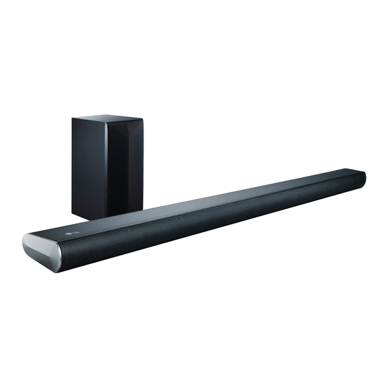
Wireless sound bar
Hide thumbs
Also See for LAS551H:
- Owner's manual (40 pages) ,
- Simple manual (8 pages) ,
- Simple manual (4 pages)
Chapters
Table of Contents

Related Manuals for LG LAS551H


Summary of Contents for LG LAS551H
- Page 1 Internal Use Only Website http://biz.lgservice.com Wireless Sound Bar SERVICE MANUAL MODEL: LAS551H (LAS551H, S55A1-D) CAUTION BEFORE SERVICING THE UNIT, READ THE “SAFETY PRECAUTIONS” IN THIS MANUAL. P/NO : AFN76932738 JANUARY, 2015...
- Page 2 CONTENTS SECTION 1 ..GENERAL SECTION 2 ..CABINET & MAIN CHASSIS SECTION 3 ..ELECTRICAL SECTION 4 ..WIRELESS SUBWOOFER PART SECTION 5 ..REPLACEMENT PARTS LIST...
-
Page 3: Table Of Contents
SECTION 1 GENERAL CONTENTS ESD PRECAUTIONS ............................1-3 WIRELESS SUBWOOFER CONNECTION ....................... 1-4 HIDDEN KEY MODE ............................1-5 MCS / EQ HIDDEN KEY GUIDE ........................1-6 MCS / EQ PROGRAM UPDATE GUIDE ......................1-7 SPECIFICATIONS ............................. 1-8... -
Page 4: Esd Precautions
ESD PRECAUTIONS Electrostatically Sensitive Devices (ESD) Some semiconductor (solid state) devices can be damaged easily by static electricity. Such components commonly are called Electrostatically Sensitive Devices (ESD). Examples of typical ESD devices are integrated circuits and some field-effect transistors and semiconductor chip components. The following techniques should be used to help reduce the incidence of component damage caused by static electricity. -
Page 5: Wireless Subwoofer Connection
WIRELESS SUBWOOFER CONNECTION LED indicator of wireless subwoofer - The LED of the wireless subwoofer lights up alternately in red and yellow-green. 4. Disconnect the power cord of the main unit and the LED Color Status wireless subwoofer. Yellow-green 5. Connect them again after the LED of the main unit The connection is trying. -
Page 6: Hidden Key Mode
HIDDEN KEY MODE HIDDEN MODE KEYS EEPROM EDIT Main set ‘-’ (Volume) + Remote control ‘OPTICAL’ EEPROM CLEAR (Initialize) Main set ‘-’ (Volume) + Remote control ‘SOUND EFFECT’ VERSION CHECK Main set ‘-’ (Volume) + Remote control ‘Play’ CLIP OFF CLIP ON Main set ‘-’... -
Page 7: Mcs / Eq Hidden Key Guide
MCS / EQ HIDDEN KEY GUIDE 1. Version & Option Check 1) Power on. 2) Press main set "-" (volume -) key and remote control " " (Play/Pause) key during 3 seconds. 3) Check MCS version. P1411182 4) Press remote control (" ") key 1 time. Check Wireless Tx version. -
Page 8: Mcs / Eq Program Update Guide
MCS / EQ PROGRAM UPDATE GUIDE 1. Preparation - Remote control. - Do format USB Memory to FAT32 File system. - USB : Update fi le exist only in the USB Memory stick. Ex ) LAS550H : E:\PG540_FW_LAS550H_Ver.bin (if USB driver is E:\) ... -
Page 9: Specifications
SPECIFICATIONS • GENERAL (LAS551H) Power requirements 120 V ~ 60 Hz Power consumption 27 W Networked standby : 2.5 W (If all network ports are activated.) Dimensions (W x H x D) 890 mm x 51 mm x 85 mm (31.8 inch x 2.0 inch x 3.3 inch) Net Weight (Approx.) - Page 10 SECTION 2 CABINET & MAIN CHASSIS CONTENTS DISASSEMBLY INSTRUCTIONS ........................2-2 EXPLODED VIEWS ............................2-5 1. MAIN SET SECTION ..........................2-5 2. WIRELESS SUBWOOFER SECTION ...................... 2-7 3. PACKING ACCESSORY SECTION ......................2-9...
-
Page 11: Disassembly Instructions
DISASSEMBLY INSTRUCTIONS Before you begin, position the main set upside down. 1. Case Bottom Assembly 1) Remove the 18 screws on the main set. 2) Remove the Case Bottom Assembly. Case Bottom Assembly Fig. 1 2. Deco Side 1) Remove the 4 screws securing the Deco Side. 2) Remove the Deco Side (left/ right). - Page 12 3. Grille 1) Remove the Grille. Fig. 3 4. Bluetooth Module 1) Disconnect the FFC cable from the Bluetooth Module. 2) Remove the Bluetooth Module. 3) Check and Replace the Bluetooth Module. Bluetooth Module Fig. 4...
- Page 13 5. Tack Key Board 1) Remove the 2 screws securing the Cover Button Assembly. 2) Remove the Cover Button Assembly (Cover Button + Holder Button). 3) Remove the Tack Key Board. 4) Disconnect the Harness cable from the Tack Key Board. 5) Check and Replace the Tack Key Board.
-
Page 14: Exploded Views
EXPLODED VIEWS 1. MAIN SET SECTION NOTES) THE EXCLAMATION POINT WITHIN AN EQUILATERAL TRIANGLE IS INTENDED TO ALERT THE SERVICE PERSONNEL TO THE PRESENCE OF IMPORTANT SAFETY INFORMATION IN SERVICE LITERATURE. A44B SPK703 CABLE2 SMPS MAIN A44A SPK704 WIRELESS FRONT HDMI &... -
Page 15: Wireless Subwoofer Section
2. WIRELESS SUBWOOFER SECTION NOTES) THE EXCLAMATION POINT WITHIN AN EQUILATERAL TRIANGLE IS INTENDED TO ALERT THE SERVICE PERSONNEL TO THE PRESENCE OF IMPORTANT SAFETY INFORMATION IN SERVICE LITERATURE. A900 A900W CN901 A47W SMPS A49W A54W A45W WIRELESS 300W... -
Page 16: Packing Accessory Section
3. PACKING ACCESSORY SECTION 806 Optical cable 801 Owner’s manual 808 Batteries (2) 829 Cable tie 835 Wall bracket 836 Screws (2) 837 Cover foot (2) 900 Remote control 804 Bag 803 Packing, Main 802 Box... - Page 17 2-10...
- Page 18 SECTION 3 ELECTRICAL CONTENTS ONE POINT REPAIR GUIDE ..........................3-2 1. NO POWER PROBLEM (PVDD) ......................3-2 2. POWER ON ERROR ..........................3-3 3. NO SOUND (PORTABLE FUNCTION) ....................3-4 4. NO WIRELESS ............................3-5 5. NO BLUETOOTH ............................ 3-6 6.
-
Page 19: One Point Repair Guide
ONE POINT REPAIR GUIDE 1. NO POWER PROBLEM (PVDD) No power problem occurs when you power on the unit 1-1. Solution Replace SMPS board. 1-2. How to troubleshoot (Countermeasure) 1) Check the PVDD voltage 18.7 V at pin1, 2, 3. When you check the no power at this point, then replace SMPS board. -
Page 20: Power On Error
ONE POINT REPAIR GUIDE 2. POWER ON ERROR No display or Not working. 2-1. IC601 1) Check 3.3 VA at L602. 2) If 3.3 VA is not checked at the point, then find 18.7 V at pin7 of IC601. 3) 1), 2) is NG. Replace IC601. L602 L602 IC601 pin7... -
Page 21: Sound (Portable Function)
ONE POINT REPAIR GUIDE 3. NO SOUND (PORTABLE FUNCTION) 3-1. Solution Replace IC508 or portable jack (JK851). 3-2. How to troubleshoot (Countermeasure) 1) Please check the soldering status of JK851. 2) Please check L854, L855 (PORT_L, PORT_R signal) of portable jack (JK851). If you cannot find input signal, replace JK851. -
Page 22: Wireless
ONE POINT REPAIR GUIDE 4. NO WIRELESS 4-1. Solution Replace IC505 on MAIN board.(No 3.3 V) 4-2. How to troubleshoot (Countermeasure) 1) Please check externally status of Wireless board to board connection on your eyes. (at CN506 and Wireless module) 2) Please check 3.3 V of WL_3V3 (at L509). -
Page 23: Bluetooth
ONE POINT REPAIR GUIDE 5. NO BLUETOOTH 5-1. Solution Replace IC502 on MAIN board.(No 3.3 V) 5-2. How to troubleshoot (Countermeasure) 1) Please check externally status of Bluetooth cable connection on your eyes.(at CN508 and Bluetooth module) 2) Please check 3.3 V of 3.3VA (at L504). If 3.3 V is OK at L509, please check BT_SDA, BT_SCL, BT_RST (pin53, 51, 25) of IC502 and BT_RX, BT_TX (pin29, 27). -
Page 24: Sound (Usb)
ONE POINT REPAIR GUIDE 6. NO SOUND (USB) 6-1. Solution Replace IC502 on MAIN board. 6-2. How to troubleshoot (Countermeasure) 1) Please check USB voltage (5 V) of JK853 (pin1) and CA851 in HDMI & JACK board. 2) Please check USB data signal (D-, D+) of IC502. (to check TP588, TP589 at CN507) If you have not data signal, please replace IC502. -
Page 25: Sound (Optical)
ONE POINT REPAIR GUIDE 7. NO SOUND (OPTICAL) 7-1. Solution Replace IC507 on MAIN board. 7-2. How to troubleshoot (Countermeasure) 1) Please check 3.3 V of 3.3VA at L853 in HDMI & JACK board If you can check 3.3 V, please confirm OPT_DET signal (R5R8) in MAIN board when optical mode. 2) In spite of process 1), set has abnormal output, then replace IC507. -
Page 26: Hdmi Problem
ONE POINT REPAIR GUIDE 8. HDMI PROBLEM No display or No Sound. 8-1. HDMI jack connection 1) Check the HDMI jack connection correctly each port. (JK801 : HDMI IN, JK800 : HDMI OUT) JK800 JK800 JK801 JK801 < HDMI & JACK board top view > 8-2. -
Page 27: Waveforms Of Major Check Point
WAVEFORMS OF MAJOR CHECK POINT 1. CRYSTAL FIG 1-1. X501 (24 MHz) FIG 1-2. X502, X701 (24.576 MHz) FIG 1-3. X801 (27 MHz) 3-10... -
Page 28: Flash Memory
2. FLASH MEMORY FIG 2. VCC, CS#, CLK, DO 3-11... -
Page 29: Tact Key
3. TACT KEY 1 ~ 1.13 V 0.72 ~ 0.82 V FIG 3-1. Press Power Key FIG 3-2. Press FUNC Key 0.424 ~ 0.485 V FIG 3-3. Press VOL - Key FIG 3-4. Press VOL + Key 3-12... -
Page 30: Usb
4. USB FIG 4-1. USB_5V FIG 4-2. USB D+ FIG 4-3. USB D- 3-13... -
Page 31: Remote Control
5. REMOTE CONTROL 16 17 FIG 5-1. Input Voltage FIG 5-2. Low Timing Item Measured Spec. IR Receiver Spec: Input Level 3.3 V 2.7 ~ 5.5 V “ Low” Timing 4.4 ms 3.6 ms ~ 5.04 ms “ High” Timing 4.48 ms 4.08 ms ~ 5.04 ms FIG 5-3. -
Page 32: Optical
6. OPTICAL FIG 6-1. OPT_IN FIG 6-2. OPT_DET 3-15... -
Page 33: Portable
7. PORTABLE FIG 7-1. ADC IC 5 V FIG 7-2. ADC IC 3.3 V FIG 7-3. Analog Input Voltage 3-16... -
Page 34: Audio Pwm
8. AUDIO PWM(1/2) FIG 8-1. PWM IC 3.3 V FIG 8-2. PWM IC 1.2 V FIG 8-3. BCK FIG 8-4. LRCK 3-17... - Page 35 AUDIO PWM(2/2) TWL+ TWL- FL+ FL- 384.14 kHz 384.14 kHz FIG 8-5. Tweeter L FIG 8-6. Front L TWR+ TWR- 384.17 kHz FIG 8-7. Tweeter R FR+ FR- 384.17 kHz FIG 8-8. Front R 3-18...
-
Page 36: Audio Amp
9. AUDIO AMP PVDD: 18.7 V FIG 9-1. AMP IC PVDD PVDD GVDD AMP_PDN FIG 9-2. 3-19... - Page 37 3-20...
-
Page 38: Wiring Diagram
WIRING DIAGRAM CN301, SMD, 4P (Harness) TACK KEY <-> MAIN TACK KEY PCB CN200, SMD, 10P (FPC), MAIN <-> LCD Module LCD Module FRONT PCB SMD, 12P, B to B CN703, CN501 (MAIN) <-> CN201(FRONT) SMD, 4P SMD, 26P, B to B (Audio L) CN507 (MAIN) <->... -
Page 39: Block Diagram
LRCK/BCK/TX_ADATA2 Offset Gain POWER/FUNC/VOL+/- PWM SDA/SCL FL/FR Controller PWM RST TAS5612 TX_LRCK TX_BCK Audio Delay TX_ADATA0 PS9860 TX_ADATA1 USER EQ LG Post PP TX_ADATA2 AFRICA LCD_CLK 24bit Max/Min LCD_STB Trunc. LCD_BL_CTRL Scaling AMP_FAULT/CLIP0/AMP_PROTECT LCD_DO [+36dB]] CLIP1 LGPP_DOW Tweeter L/R NMIX_221... -
Page 40: Circuit Diagrams
DIFFER FROM THE ACTUAL CIRCUIT USED. THIS 2. Voltages are DC-measured with a digital voltmeter 1. SMPS CIRCUIT DIAGRAM PERMISSION FROM THE LG CORPORATION. ALL WAY, IMPLEMENTATION OF THE LATEST SAFETY during Play mode. COMPONENTS SHOULD BE REPLACED ONLY WITH... -
Page 41: Main - Dsp Circuit Diagram
2. MAIN - DSP CIRCUIT DIAGRAM : WAVEFORM NUMBER EAX66222601 Rev1.7(24) MAIN(#2) 2014.11.26 3-27 3-28... -
Page 42: Main - Pwm & Amp Circuit Diagram
3. MAIN - PWM & AMP CIRCUIT DIAGRAM PWM & AMP : WAVEFORM NUMBER EAX66222601 Rev1.7(24) MAIN(#3) 2014.11.26 3-29 3-30... -
Page 43: Main - Power Circuit Diagram
4. MAIN - POWER CIRCUIT DIAGRAM POWER EAX66222601 Rev1.7(19) MAIN(#4) 2014.11.26 3-31 3-32... -
Page 44: Hdmi & Jack Circuit Diagram
5. HDMI & JACK CIRCUIT DIAGRAM HDMI & JACK : WAVEFORM NUMBER EAX66225501 Rev1.7(24) 2014.11.26 3-33 3-34... -
Page 45: Front Circuit Diagram
6. FRONT CIRCUIT DIAGRAM 16 17 FRONT : WAVEFORM NUMBER EAX66226401 Rev1.7(19) 2014.11.26 3-35 3-36... -
Page 46: Tact Key Circuit Diagram
7. TACT KEY CIRCUIT DIAGRAM TACK KEY EAX66226501 Rev1.7(24) 2014.11.26 3-37 3-38... -
Page 47: Circuit Voltage Chart
CIRCUIT VOLTAGE CHART Designator Description Voltage Spec Measured Voltage Designator Description Voltage Spec Measured Voltage CONNECTORS IC501 IC,Serial Flash Memory 3.3 VA 3.4 V 5.17 V 1, 20, 43, 90, 132, 158 3.3 VA (IO) 3.34 V CN501 Connector, B to B 12 V 12.03 V 57, 60, 164... -
Page 48: Printed Circuit Board Diagrams
PRINTED CIRCUIT BOARD DIAGRAMS 1. SMPS P. C. BOARD DIAGRAM (TOP VIEW) NOTE) Warning Parts that are critical with respect to risk of fire or electrical shock. (BOTTOM VIEW) 3-41 3-42... -
Page 49: Main P. C. Board Diagram
2. MAIN P. C. BOARD DIAGRAM (TOP VIEW) (BOTTOM VIEW) 3-43 3-44... -
Page 50: Hdmi & Jack P. C. Board Diagram
3. HDMI & JACK P. C. BOARD DIAGRAM (TOP VIEW) (BOTTOM VIEW) 4. FRONT P. C. BOARD DIAGRAM (TOP VIEW) (BOTTOM VIEW) 5. TACT KEY P. C. BOARD DIAGRAM (TOP VIEW) (BOTTOM VIEW) 3-45 3-46... - Page 51 3-47 3-48...
- Page 52 SECTION 4 WIRELESS SUBWOOFER PART CONTENTS ONE POINT REPAIR GUIDE ..........................4-2 1. NO POWER PROBLEM (PVDD) ......................4-2 2. POWER ON ERROR ..........................4-3 3. POWER ON ERROR ..........................4-4 4. WIRELESS CONNECTION ........................4-5 WAVEFORMS OF MAJOR CHECK POINT ...................... 4-6 1.
-
Page 53: One Point Repair Guide
ONE POINT REPAIR GUIDE 1. NO POWER PROBLEM (PVDD) No power problem occurs when you power on the unit 1-1. Solution If you check these points and find PVDD voltage is not checked, replace woofer SMPS board. 1-2. Service hint (Any picture / Remark) PVDD PVDD pin3, 4, 5, 6 at WCN601... -
Page 54: Power On Error
ONE POINT REPAIR GUIDE 2. POWER ON ERROR Fundamental power check points 2-1. 12 V 1) Check 12 V at WL604 nearby WL603 coil. 2) If 12 V is not checked at the point, then find PVDD at pin7 of WIC606. 3) 1), 2) is NG ... - Page 55 ONE POINT REPAIR GUIDE 3. POWER ON ERROR MAIN SoC IC supply voltage check points 3-1. 3.3 VA 1) Check 3.3 VA at WCA603 and WL627. 2) Check 3.3V_PWM at pin5 of WIC605. 3) Check 3.3 VA at pin7, 8 of WIC603. 4) Check 3.3V_PWM at WL615 nearby WIC601.
-
Page 56: Wireless Connection
ONE POINT REPAIR GUIDE 4. WIRELESS CONNECTION Wireless connection malfunction 4-1. 3.3 VA 1) Check 3.3 VA at WL616. 4-2. Connection 1) Wireless module connection closely. 2) Implement Wireless Factory Reset. MAIN SET : Soundbar vol MIN and push Mute key (sustain 3 ~ 5 sec). ... -
Page 57: Waveforms Of Major Check Point
WAVEFORMS OF MAJOR CHECK POINT 1. VOLTAGE FIG 1-1. WIC607 3.7 VA FIG 1-2. PWM 3.3 V FIG 1-3. Wireless 3.3 VA... -
Page 58: Amp Voltage
2. AMP VOLTAGE PVDD: 34.5 V FIG 2-1. Woofer PVDD FIG 2-2. Woofer 12 V... -
Page 59: Pwm
3. PWM FIG 3-1. Woofer PWM SW+ SIgnal FIG 3-2. Woofer PWM SW- SIgnal... -
Page 60: Led
4. LED FIG 4-1. Pairing Off Status Red LED FIG 4-2. Pairing On Status Yellow LED... - Page 61 4-10...
-
Page 62: Wiring Diagram
WIRING DIAGRAM WOOFER AMP Wireless module PN901, DIP, 2P WOOFER (Power Cord) WCN602, SMD, 24P, B to B CN901, Harness Cable, (Wireless module) WCN601, DIP, 10P PAIRING KEY WCN604, DIP, 2P JK401, Harness Cable, WCN603, DIP, 2P WOOFER SMPS PCB (SWF) WCN605, DIP, 3P (LED CNT) -
Page 63: Block Diagram
BLOCK DIAGRAM PVDD PWM_SW+ WOOFER PWM_SW- WOOFER PWM 3.3 3.7 V PVDD DC-DC 12 V Wireless 3.3 Flash PVDD DC-DC 4-13 4-14... -
Page 64: Circuit Diagrams
DIFFER FROM THE ACTUAL CIRCUIT USED. THIS 2. Voltages are DC-measured with a digital voltmeter 1. WOOFER SMPS CIRCUIT DIAGRAM PERMISSION FROM THE LG CORPORATION. ALL WAY, IMPLEMENTATION OF THE LATEST SAFETY during Play mode. COMPONENTS SHOULD BE REPLACED ONLY WITH... -
Page 65: Woofer Amp Circuit Diagram
2. WOOFER AMP CIRCUIT DIAGRAM WF-AMP : WAVEFORM NUMBER EAX66304701 Rev1.2(7) 2014.11.26 4-17 4-18... -
Page 66: Woofer Key Circuit Diagram
3. WOOFER KEY CIRCUIT DIAGRAM WF-KEY EAX66305401 Rev1.2(6) 2014.11.26 4-19 4-20... -
Page 67: Printed Circuit Board Diagrams
PRINTED CIRCUIT BOARD DIAGRAMS 1. WOOFER SMPS P. C. BOARD (TOP VIEW) (BOTTOM VIEW) NOTE) Warning Parts that are critical with respect to risk of fire or electrical shock. 4-21 4-22... -
Page 68: Woofer Amp P. C. Board
2. WOOFER AMP P. C. BOARD (TOP VIEW) (BOTTOM VIEW) 3. WOOFER KEY P. C. BOARD (TOP VIEW) (BOTTOM VIEW) 4-23 4-24... - Page 69 4-25 4-26...