Table of Contents
Advertisement
Note: Please refer to the original service manual for:
DVD Mechanism Unit (BRS11D), Order No. PSG1201015AE
Speaker system SB-XH170PC-K (For SA-XH170EB/EG-K), Order No. PSG1201002CE
Speaker system SB-XH175EP-K (For SA-XH175EP-K), Order No. PSG1202026CE
TABLE OF CONTENTS
1 Safety Precautions----------------------------------------------- 3
1.1. General Guidelines---------------------------------------- 3
1.2. Before Repair and Adjustment ------------------------- 4
1.3. Protection Circuitry ---------------------------------------- 4
1.4. Caution For AC Cord (For EB only)------------------- 5
1.5. Caution For Fuse Replacement------------------------ 6
1.6. Safety Part Information----------------------------------- 7
2 Warning -------------------------------------------------------------- 8
to Electrostatic Sensitive (ES) Devices -------------- 8
2.2. Precaution of Laser Diode------------------------------- 9
2.4. Handling Precautions for Traverse Unit------------- 11
3 Service Navigation ----------------------------------------------13
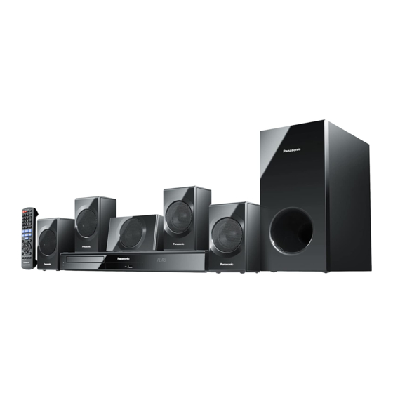
DVD Home Theater Sound System
Model No.
Product Color: (K)...Black Type
PAGE
3.1. Service Information -------------------------------------- 13
4 Specifications ---------------------------------------------------- 14
4.1. Others (Licences) ---------------------------------------- 15
5 General/Introduction------------------------------------------- 16
5.1. Power-Saving Features -------------------------------- 16
5.3. Disc Information ------------------------------------------ 18
5.4. DivX Information------------------------------------------ 19
6 Location of Controls and Components------------------ 20
6.1. Remote Control Key Button Operations------------ 20
6.2. Main Unit Key Button Operations -------------------- 21
7 Installation Instructions -------------------------------------- 22
7.1. Speaker Connections ---------------------------------- 22
© Panasonic Corporation 2012. All rights reserved.
Unauthorized copying and distribution is a violation
of law.
SA-XH170EB
SA-XH170EG
SA-XH175EP
PSG1202014CE
PAGE
Advertisement
Table of Contents
Troubleshooting

Related Manuals for Panasonic SA-XH170EB


Summary of Contents for Panasonic SA-XH170EB
-
Page 1: Table Of Contents
Product Color: (K)...Black Type Note: Please refer to the original service manual for: DVD Mechanism Unit (BRS11D), Order No. PSG1201015AE Speaker system SB-XH170PC-K (For SA-XH170EB/EG-K), Order No. PSG1201002CE Speaker system SB-XH175EP-K (For SA-XH175EP-K), Order No. PSG1202026CE TABLE OF CONTENTS PAGE... - Page 2 7.2. Radio Antenna Connection ---------------------------- 22 17.1. Schematic Diagram Notes ---------------------------- 91 7.3. Connection with an ARC compatible TV ----------- 23 17.2. Main(HDMI/Micon) Circuit ----------------------------- 93 8 Operating Instructions ---------------------------------------- 24 17.3. Panel Circuit --------------------------------------------- 104 8.1. Removing of disc during abnormality --------------- 24 17.4.
-
Page 3: Safety Precautions
1 Safety Precautions 1.1. General Guidelines 1. When servicing, observe the original lead dress. If a short circuit is found, replace all parts which have been overheated or damaged by the short circuit. 2. After servicing, see to it that all the protective devices such as insulation barriers, insulation papers shields are properly installed. -
Page 4: Before Repair And Adjustment
1.2. Before Repair and Adjustment Disconnect AC power to discharge unit AC Capacitors as such (C5700, C5701, C5702, C5704, C5705, C5706) through a 10 Ω, 10 W resistor to ground. Caution: DO NOT SHORT-CIRCUIT DIRECTLY (with a screwdriver blade, for instance), as this may destroy solid state devices. After repairs are completed, restore power gradually using a variac, to avoid overcurrent. -
Page 5: Caution For Ac Cord (For Eb Only)
1.4. Caution For AC Cord (For EB only) -
Page 6: Caution For Fuse Replacement
1.5. Caution For Fuse Replacement... -
Page 7: Safety Part Information
1.6. Safety Part Information Safety Parts List: There are special components used in this equipment which are important for safety. These parts are marked by in the Schematic Diagrams, Exploded View & Replacement Parts List. It is essential that these critical parts should be replaced with manufacturer’s specified parts to prevent shock, fire or other hazards. -
Page 8: Warning
2 Warning 2.1. Prevention of Electrostatic Discharge (ESD) to Electrostatic Sensitive (ES) Devices Some semiconductor (solid state) devices can be damaged easily by static electricity. Such components commonly are called Elec- trostatically Sensitive (ES) Devices. Examples of typical ES devices are integrated circuits and some field-effect transistors and semiconductor “chip”... -
Page 9: Precaution Of Laser Diode
2.2. Precaution of Laser Diode Caution: This product utilizes a laser diode with the unit turned “on”, invisible laser radiation is emitted from the pickup lens. Wavelength: 655 nm (DVD)/790 nm (CD) Maximum output radiation power from pickup: 100 µW/VDE Laser radiation from the pickup unit is safety level, but be sure the followings: 1. -
Page 10: Service Caution Based On Legal Restrictions
2.3. Service caution based on Legal restrictions 2.3.1. General description about Lead Free Solder (PbF) The lead free solder has been used in the mounting process of all electrical components on the printed circuit boards used for this equipment in considering the globally environmental conservation. The normal solder is the alloy of tin (Sn) and lead (Pb). -
Page 11: Handling Precautions For Traverse Unit
2.4. Handling Precautions for Traverse Unit The laser diode in the optical pickup unit may break down due to static electricity of clothes or human body. Special care must be taken avoid caution to electrostatic breakdown when servicing and handling the laser diode in the traverse unit. Cautions to Be Taken in Handling the Optical Pickup Unit 2.4.1. - Page 12 Grounding for electrostatic breakdown prevention 2.4.2. Some devices such as the DVD player use the optical pickup (laser diode) and the optical pickup will be damaged by static electric- ity in the working environment. Proceed servicing works under the working environment where grounding works is completed. 2.4.2.1.
-
Page 13: Service Navigation
3 Service Navigation 3.1. Service Information This service manual contains technical information which will allow service personnel’s to understand and service this model. Please place orders using the parts list and not the drawing reference numbers. If the circuit is changed or modified, this information will be followed by supplement service manual to be filed with original service manual. -
Page 14: Specifications
4 Specifications 1 Vp-p (75 Ω) Y output level PAL; 0.3 Vp-p (75 Ω) C output level Main unit NTSC; 0.286 Vp-p (75 Ω) AMPLIFIER SECTION Terminal SCART (1 system) RMS Output Power: Dolby Digital Mode RGB video output Front Ch 0.7 Vp-p (75 Ω) R output level 160 W per channel (3 Ω), 1 kHz, 10% THD... -
Page 15: Others (Licences)
4.1. Others (Licences) -
Page 16: General/Introduction
5 General/Introduction 5.1. Power-Saving Features... -
Page 17: Linked Operations With The Tv (Viera Link™ "Hdavi Control™")
5.2. Linked Operations with the TV (VIERA Link™ “HDAVI Control™”) -
Page 18: Disc Information
5.3. Disc Information 5.3.1. Discs that can be played... -
Page 19: Divx Information
5.3.2. File Extension Type Support (MP3/JPEG/DivX) 5.4. DivX Information... -
Page 20: Location Of Controls And Components
6 Location of Controls and Components 6.1. Remote Control Key Button Operations... -
Page 21: Main Unit Key Button Operations
6.2. Main Unit Key Button Operations... -
Page 22: Installation Instructions
7 Installation Instructions Turn off all equipment before connection and read the appropriate operating instructions. Do not connect the AC mains lead until all other connections are completed. 7.1. Speaker Connections 7.2. Radio Antenna Connection... -
Page 23: Connection With An Arc Compatible Tv
7.3. Connection with an ARC compatible TV... -
Page 24: Operating Instructions
8 Operating Instructions 8.1. Removing of disc during abnormality 8.1.1. Using main unit key buttons. 8.1.1.1. When the power can be turned off. 1. Turn off the power and press & hold [OPEN/CLOSE] button on main unit and [SKIP FWD] button on remote for 5 seconds 8.1.1.2. - Page 25 3. Gently pull out the tray. 4. Remove disc...
-
Page 26: Playing From An Usb Device
8.2. Playing From an USB Device... -
Page 27: Service Mode
9 Service Mode 9.1. Cold-Start Here is the procedure to carry out cold-start for initialize to shipping mode. 1. Unplug AC power cord 2. Press & hold [ ] button 3. Plug AC power cord while [ ] button being pressed FL Display will show “_ _ _ _ _ _ _ _”... - Page 28 Product Series Country Region Broadcasting Selected Region Display Code OSD Menu Language Code System TV System (Default) Default USA, Canada, English (NA), Spanish (NA), P, PC, PX, NTSC AUTO2 (*A) English US Military Canadian French (blank) Japan NTSC AUTO2 (*A) Japanese Japanese, English English (EU), French, German,...
- Page 29 9.2.2. Setting of Panel Code Step1 : Press [OPEN/CLOSE] button on main unit, follow by [4] and [7] on remote control (To enter Doctor Mode). Step2 : Press [CANCEL] button on remote control, then press [2], [2], [8] and [0] on remote control. Step3 : Key in new panel code using remote control (refer to Figure 9.2.2).
-
Page 30: Self Diagnostic
9.3. Self Diagnostic By pressing various button combinations on the main unit and remote control unit, you can activate the various service modes for checking. Special Note: • Due to the limitations of the no. characters that can be shown on the FL Display, the “FL Display” button on the remote control unit can be used to show the two display pages. - Page 31 9.3.2. Self Diagnostic Table 2 (For DVD) Item Key Operation FL Display Mode Name Description Front Key DVD laser DVD laser drive current measurement. In STOP (no disc) mode, drive current For DVD laser drive current, refer to press [OPEN/CLOSE] measurement Troubleshooting Guide (Section 10.2) button on the main unit,...
- Page 32 9.3.3. Self Diagnostic Table 3 (For DVD) Item Key Operation FL Display Mode Name Description Front Key Micro-processor Micro-processor firmware version In STOP (no disc) (Display 1) firmware version display & EEPROM checksum display. mode, press display & EEPROM checksum is only available [OPEN/CLOSE] button on EEPROM due to existence of EEPROM IC.
- Page 33 9.3.4. Self Diagnostic Table 4 (For DVD) Item Key Operation FL Display Mode Name Description Front Key Region and DVD firmware version is displayed on In STOP (no disc) Firmware the FL Display. mode, press version display [OPEN/CLOSE] button on the main unit, and [8] button on the remote control unit.
- Page 34 9.3.5. Self Diagnostic Table 5 Item Key Operation FL Display Mode Name Description Front Key Press & hold Self-Diagnostic To enter into self-diagnostic checking [OPEN/CLOSE] on main Mode unit, follow by [4] then [9] on remote control. (When no disc in tray) Error code will display Error code System will perform a check on...
-
Page 35: Error Code
9.4. Error Code 9.4.1. Error Code Table 1 Error Diagnosis Description of error Automatic FL Display Remarks Code Contents The abnormalities In normal operation, when DCDET2 goes to Press [OPEN/CLOSE] in the Power Amp L, immediately PCNT is set to L (not normal on main unit for next output or power POWER OFF sequence), and Error Code... - Page 36 9.4.2. Error Code Table 2 Error Diagnosis Description of error Automatic FL Display Remarks Code Contents The tray opening and closing is abnormal. Press [OPEN/CLOSE] on Tray loading error CLOSE and OPEN of the tray cannot be main unit for next error. carried out properly.
-
Page 37: Sales Demonstration Lock Function
9.5. Sales Demonstration Lock Function This function prevents discs from being lost when the unit is used for sales demonstrations by disabling the disc eject function. “LOCKED” is displayed on the unit, and ordinary operation is disabled. 9.5.1. Setting • Prohibiting removal of disc 1. -
Page 38: Firmware Version-Up Information
9.6. Firmware Version-Up Information 9.6.1. Process Flow (1/2) Item FL/ GUI Display Remarks Process Description Collect ROM Step 1 Display 1: User can put both files Files Unzip the firmware update file. into the same root (Copy files into Step 2 directory. - Page 39 9.6.2. Process Flow (2/2) Item FL/ GUI Display Remarks Process Description GUI Display 1.3: To initialize, press and hold Update Completed main unit [OPEN/CLOSE] If firmware software update then press remote control completes successfully: key [ 10]. GUI Display 1.3: "Firmware update is completed, please open the tray and remove the disc."...
-
Page 40: Troubleshooting Guide
10 Troubleshooting Guide 10.1. Troubleshooting Guide for F61 and/or F76 This section illustrates the checking procedures when upon detecting the error of “F61” and/or “F76” after power up of the unit. It is for purpose of troubleshooting and checking in SMPS P.C.B.. Symptom(s) Checking items Possible Fault(s) - Page 41 10.1.1. SMPS P.C.B. Transformer: T5701 Photocoupler: PC5720 Switching IC: IC5701 Thermal Diode: D5802 Photocoupler: Switching IC: IC5799 PC5702, PC5799 Fig. 1. SMPS P.C.B.
- Page 42 10.1.2. Main P.C.B (Side A of Main P.C.B.) Q2902 Q2903, L2908 IC2901, L2902, (Side B of Main P.C.B.) R2399 LB2761 L2904, Q2904 Fig. 2. Main P.C.B.
-
Page 43: Dvd/Cd Laser Diode Current Measurement
10.2. DVD/CD Laser Diode current measurement This section will illustrate proceddures of measuring & deriving DVD/CD Laser Diode Current. Item Description Checking Item/Formula Remarks 1. Measurement the voltage (V ) on the testpoints CL8530(+) & CL8531(-). Refer to 10.1.2. CD Laser Diode Current Measurement Main P.C.B. -
Page 44: Basic Troubleshooting Guide For Traverse Unit (Main P.c.b.)
10.3. Basic Troubleshooting Guide for Traverse Unit (Main P.C.B.) Problems Checking Points Checking components 1) Distorted picture or a) Check SDRAM address, data IC8051 abnormal sound is head bus, CLK and other control signals during the initialization waveform b) Check video signals (CVBS) LB8317, R8325, IC8011 (Pin 63) c) Check audio DAC circuitry LB8422 till LB8428... -
Page 45: Basic Troubleshooting Guide For Hdmi Av Output
10.4. Basic Troubleshooting Guide for HDMI AV output Problems Checking Points Checking components 1) TV does not have any 1) Check setting of the set in * This year HDMI always ON. display. Set FL display shows Setup Menu whether the HDMI No need to check Setup Menu. -
Page 46: Service Fixture & Tools
11 Service Fixture & Tools Prepare service tools before process service position. Ref. No Service Tools Remarks SFT1 Main P.C.B. (CN2006) - D-Amp P.C.B. (CN5402) RFKZBTT270K3 (18P FFC) -
Page 47: Disassembly And Assembly Instructions
12 Disassembly and Assembly Instructions Caution Note: • This section describes the disassembly and/or assembly procedures for all major printed circuit boards & main compo- nents for the unit. (You may refer to the section of “Main components and P.C.B Locations” as described in the service manual) •... -
Page 48: Disassembly Flow Chart
12.2. Disassembly Flow Chart Main Unit 12.4. Top Cabinet 12.5. Tray Ornament 12.22. DVD Mechanism 12.6. Front Panel Block 12.10. Rear Panel Unit (BRS11D) Assembly 12.7. Operation Button 12.11. Fan 12.23. Traverse Unit P.C.B. 12.8. Power Button 12.12. Main P.C.B. P.C.B. -
Page 49: Main Components And P.c.b. Locations
12.3. Main Components and P.C.B. Locations... -
Page 50: Disassembly Of Top Cabinet
12.4. Disassembly of Top Cabinet Step 4 Slightly lift both sides of Top Cabinet in an outward direction about 30°. Step 1 Remove 2 screws. Caution: Ensure that the angle from Top Cabinet to bottom chassis is not greater than 30°. Step 2 Remove 3 screws. -
Page 51: Replacement Of Tray Ornament
Step 5 Press the catches and remove the Top Cabinet as arrow 12.5. Replacement of Tray Ornament shown in sequence. Step 1 Use a Paper Clip and insert into the hole on the bottom Caution: Avoid touching electrical components when hand of the unit. - Page 52 Step 4 Release 2 catches. Caution: During assembling, ensure that the Tray Orna- ment's guide rib is fully catched onto the Tray. Caution: During assembling, ensure that the Tray Orna- ment is inserted & fully catched onto Tray. Step 5 Remove Tray Ornament in the direction of arrow. Step 6 Slide the Tray in fully.
-
Page 53: Disassembly Of Front Panel Block Assembly
12.6. Disassembly of Front Panel Step 3 Release the 3 tabs at the Bottom Chassis. Caution: Do not exert strong force when releasing the tabs. Block Assembly • Refer to “Disassembly of Top Cabinet”. • Refer to "Replacement of Tray Ornament". Step 1 Detach 4P Cable at the connector (CN6001) on Panel P.C.B.. -
Page 54: Disassembly Of Operation Button P.c.b
Step 4 Remove the Front Panel Block Assembly. Step 2 Release 3P Cable from ribs of Front Panel. Caution: During assembling, dressed the 3P Cable in the ribs of Front Panel Block Assembly. 12.7. Disassembly of Operation But- ton P.C.B. •... -
Page 55: Disassembly Of Power Button P.c.b
Step 4 Desolder 3P Cable at the cable holder (H6003) on Step 2 Release 3P Cable from ribs of Front Panel. Operation Button P.C.B.. Caution: During assembling, dressed the 3P Cable in the ribs of Front Panel Block Assembly. Step 5 Remove the Operation Button P.C.B.. Step 3 Lift up the Power Button P.C.B.. -
Page 56: Disassembly Of Panel P.c.b
Step 4 Release 2 catches. 12.9. Disassembly of Panel P.C.B. Step 5 Remove the Led Holder. • Refer to “Disassembly of Top Cabinet”. • Refer to "Replacement of Tray Ornament". • Refer to “Disassembly of Front Panel Block Assembly”. Step 1 Detach 21P FFC at the connector (P6001) on Panel P.C.B.. -
Page 57: Disassembly Of Rear Panel
Caution: During assembling, ensure that Panel P.C.B. is Step 3 Remove the Rear Panel. properly located & fully seated onto Bottom Chassis. 12.10. Disassembly of Rear Panel 12.11. Disassembly of Fan Unit • Refer to “Disassembly of Top Cabinet” • Refer to “Disassembly of Top Cabinet” Step 1 Remove 11 screws. -
Page 58: Disassembly Of Main P.c.b
Step 3 Remove 2 screws. Step 2 Release 2 tabs at each side of the Rear Panel in the Step 4 Lift up to remove the Fan Unit. direction of arrow. Step 3 Detach 18P FFC at the connector (CN2006) on Main P.C.B.. -
Page 59: Disassembly Of D-Amp P.c.b
Step 6 Detach 5P FFC at the connector (FP8252) on Main Caution: During assembling, ensure that Main P.C.B. is properly located & fully seated onto Bottom Chassis. P.C.B.. Step 7 Detach 6P FFC at the connector (FP8251) on Main P.C.B.. Step 8 Detach 24P FFC at the connector (FP8531) on Main P.C.B.. -
Page 60: Replacement Of Digital Amplifier Ic (Ic5100/ Ic5200/Ic5300)
Step 3 Lift up the Wire Clamper. Caution: During assembling, ensure that D-Amp P.C.B. is properly located & fully seated onto Bottom Chassis. Step 4 Detach 3P Fan Wire at the connector (CN5401) on D- Amp P.C.B.. Step 5 Detach 18P FFC at the connector (CN5402) on D-Amp P.C.B.. - Page 61 Step 3 Lift up D-Amp P.C.B. as arrow shown. 12.14.2. Assembly of Digital Amplifier IC Caution: Keep the Heatsink Spacers in safe place. Avoid (IC5100/IC5200/IC5300) denting it, place it back during assembling. Step 1 Fix the Digital Amplifier IC (IC5100) onto the D-Amp P.C.B..
-
Page 62: Disassembly Of Ac Inlet P.c.b
Step 5 Upset the D-Amp P.C.B.. Step 2 Remove 2 screws. Step 6 Fix 4 screws. Step 3 Release Red Wire (TL30) and Black Wire (TL20) from Note: For assembling of Digital Amplifier IC (IC5200) & the Wire Holder. (IC5300), repeat the (Step 1) to (Step 6) of 12.14.2. Caution: During assembling, ensure that Red Wire (TL30) and Black Wire (TL20) are dressed into Wire Holder prop- erly. -
Page 63: Disassembly Of Smps P.c.b
Step 5 Flip the AC Inlet P.C.B.. Step 3 Remove 4 screws. Step 6 Desolder Red Wire (TL30) and Black Wire (TL20) on AC Step 4 Release Red Wire (TL31) and Black Wire (TL21) from Inlet P.C.B.. the Wire Holder. Step 7 Remove the AC Inlet P.C.B.. -
Page 64: Replacement Of Switching Regulator Ic (Ic5701)
Step 6 Upset the SMPS P.C.B.. 12.17. Replacement of Switching Reg- Step 7 Desolder Red Wire (TL31) and Black Wire (TL21) on ulator IC (IC5701) SMPS P.C.B.. Caution: During assembling, ensure the Red Wire (TL31) • Refer to “Disassembly of Top Cabinet”. and Black Wire (TL21) is inserted before soldering, check •... - Page 65 Step 5 Remove the Switching Regulator Unit in the direction of 12.17.2. Assembly of Switching Regulator arrow. IC (IC5701) Caution: Avoid touching the Heatsink A due to its high Step 1 Apply Grease to the back of Switching Regulator IC temperature after prolonged use.
-
Page 66: Replacement Of Diode (D5702)
Step 4 Solder pins of the Switching Regulator IC (IC5701) on 12.18. Replacement of Diode (D5702) the solder side of SMPS P.C.B.. • Refer to “Disassembly of Top Cabinet. Step 5 Solder pins of the Diode (D5702) on the solder side of •... - Page 67 Step 5 Remove the Switching Regulator Unit in the direction of 12.18.2. Assembly of Diode (D5702) arrow. Step 1 Apply Grease to the back of Diode (D5702). Caution: Avoid touching the Heatsink A due to its high Step 2 Fix and screw the Diode (D5702) to the Heatsink A. temperature after prolonged use.
-
Page 68: Replacement Of Diode (D5802)
Step 4 Solder pins of the Switching Regulator IC (IC5701) on 12.19. Replacement of Diode (D5802) the solder side of SMPS P.C.B.. • Refer to “Disassembly of Top Cabinet. Step 5 Solder pins of the Diode (D5702) on the solder side of •... -
Page 69: Replacement Of Diode (D5803)
12.19.2. Assembly of Diode (D5802) 12.20. Replacement of Diode (D5803) Step 1 Apply Grease to the back of Diode (D5802). • Refer to “Disassembly of Top Cabinet. Step 2 Fix and screw the Diode (D5802) to the Heatsink B. • Refer to “Disassembly of SMPS P.C.B.”. Caution: Ensure that Diode (D5802) is properly fixed and fully screwed onto Heatsink B. -
Page 70: Disassembly Of Scart P.c.b
12.20.2. Assembly of Diode (D5803) 12.21. Disassembly of Scart P.C.B. Step 1 Apply Grease to the back of Diode (D5803). • Refer to “Disassembly of Top Cabinet”. Step 2 Fix and screw the Diode (D5803) to the Heatsink B. Caution: Ensure that Diode (D5803) is properly fixed and Step 1 Detach 11P FFC at the connector (CN4002) on Scart fully screwed onto Heatsink B. -
Page 71: Disassembly Of Dvd Mechanism Unit (Brs11D)
Caution: During assembling, ensure that Scart P.C.B. is Step 4 Remove 4 screws. properly inserted & fully catched onto the rear panel. 12.22. Disassembly of DVD Mecha- nism Unit (BRS11D) • Refer to “Disassembly of Top Cabinet” • Refer to “Replacement of Tray Ornament” Step 1 Detach 5P FFC at the connector (FP8252) on Main P.C.B.. -
Page 72: Replacement Of Traverse Unit
Step 6 Attach a short pin to the 24P FFC of the DVD Mecha- 12.23. Replacement of Traverse unit nism. • Refer to “Disassembly of DVD Mechanism Unit (BRS11D)”. Caution: Refer to 2.4 “Handling Precaution for Traverse Unit” to prevent static damage to the Optical Pickup unit. Note: 1. - Page 73 Step 2 Slide the tray out fully. Step 4 Release the guide as shown & slide the Traverse Slide Plate to the end. Step 3 Release the catches & remove the tray. Step 5 Release the 24P FFC from the slot.
- Page 74 Step 6 Lift the Traverse Unit by approximately 45°. 12.23.2. Assembly of Traverse Unit Step 7 Slide out the traverse unit as arrow shown. Step 1 Release the guides as shown & slide the Traverse Slide Plate to the end. Caution: Avoid touching the surface of the traverse unit.
- Page 75 Step 2 Insert the Traverse unit at approximately 45° into the Step 3 Ensure the Traverse Unit seated properly onto the mecha chassis as arrow shown. Groove. Step 4 Slide Traverse Slide Plate to lock the Traverse Unit as shown.
- Page 76 Step 5 Insert the FFC onto the slot. Step 7 Insert the Tray into the Guides as picture shown. Caution: Ensure that the FFC are properly inserted into the slots as shown. Step 8 Align the Guides are align with the groove when sliding Step 6 Slide the Traverse Slide Plate until it stop at the Guide.
- Page 77 Step 9 Slide the tray in fully.
-
Page 78: Service Position
13 Service Position Step 7 Flip the Panel P.C.B. and position it onto the insulated material. Note: For description of the disassembly procedures, see Step 8 Proceed to check and repair Panel P.C.B.. the Section 12. 13.1. Checking & Repairing of Panel P.C.B. -
Page 79: Checking And Repairing D-Amp P.c.b
13.2.2. Checking Repairing Main Step 6 Flip the Main P.C.B. and position it onto the insulated material. P.C.B. (Side A) Step 7 Proceed to check and repair Side A of Main P.C.B.. Step 1 Remove Top Cabinet. Step 2 Remove Rear Panel. Step 3 Detach 18P FFC at the connector (CN2006) on Main P.C.B.. - Page 80 Step 5 Lift up D-Amp P.C.B. as arrow shown. 13.3.2. Checking and Repairing D-Amp P.C.B. (Side A) Step 1 Remove Top Cabinet. Step 2 Remove Rear Panel. Step 3 Remove 2 screws. Step 4 Flip the D-Amp P.C.B. and position it onto the insulated material.
-
Page 81: Checking & Repairing Of Smps P.c.b
13.4. Checking & Repairing of SMPS P.C.B. Step 1 Remove Top Cabinet. Step 2 Lift up the Wire Clamper. Step 3 Remove 4 screws. Step 4 Flip the SMPS P.C.B. and position it onto the insulated material. Step 5 Proceed to check and repair SMPS P.C.B.. -
Page 83: Overall Simplified Block Diagram
14 Overall Simplified Block Diagram MAIN BLOCK MICON TUNER D-AMP BLOCK HDMI HDMI D-IN Composite FRONT L FRONT R MCLK,BCLK,SRCK MCLK,BCLK,SRCK SURR L CP IC HDMI Video Buffer SURR R MCLK,BCLK,SRCK FLASH Zoran CENTER SELECTOR SDRAM Motor SUBWOOFER Driver UART +5.3V MICROPROCESSOR PCONT,ECO CTL... -
Page 84: Block Diagram
MICRO-P TX DUPRDI FP8251 INNER SW FROM/TO SFDO SYSTEM CONTROL LOADING P.C.B. FP8252 10 VOTR+ FWD 6 FP8252 9 VOTR- REV 7 FP8252 CLOSE SW CLOSE SW CLOSE SW FP8252 OPEN SW OPEN SW OPEN SW SA-XH170EB/EG,SA-XH175EP BACKEND BLOCK DIAGRAM... -
Page 85: Ic Terminal Chart
MDQ 4 MDQ 5 MDQ 6 MDQ 7 MDQ 8 MDQ 9 DQ10 MDQ 10 DQ10 DQ11 MDQ 11 DQ11 DQ12 MDQ 12 DQ12 DQ13 MDQ 13 DQ13 DQ14 MDQ 14 DQ14 DQ15 MDQ 15 DQ15 SA-XH170EB/EG,SA-XH175EP IC TERMINAL CHART... -
Page 86: System Control
6 SCL D2554 SWITCH Q2555 Q2557 FUNCTION SW VIDEO VMUTE2 FUNCTION SW SWITCH +12V 50 VMUTE2 MUTING XIN(32K) 13 X2300 XOUT(32K) 11 QR2002 RGB H SWITCH RGB H 3.3V QR2001 RGB H SWITCH 49 RGB H SA-XH170EB/EG,SA-XH175EP SYSTEM CONTROL BLOCK DIAGRAM... -
Page 87: Audio & Video
D5403 C0ABBA000168 FAN UNIT DUAL OP-AMP FROM/TO Q5400,Q5403 SYSTEM CONTROL FROM DCDET DCDET POWER SUPPLY CN5401 CONTROL FAN DC OUT CIRCUIT FAN DA FAN DA CN2006 CN5402 FAN DA FAN LOCK CN5401 FAN DA SA-XH170EB/EG,SA-XH175EP AUDIO & VIDEO BLOCK DIAGRAM... -
Page 88: Power Supply
DCDET DCDET FB 6 AUDIO & VIDEO D5407 H5700 CN5400 +35V +35V +35V PC5704 FEEDBACK D5703 D5707 FEEDBACK CIRCUIT IC5802 C0DBZYY00490 SHUNT REGULATOR PRIMARY SECONDARY NOTE: “ * ” REF IS FOR INDICATION ONLY SA-XH170EB/EG,SA-XH175EP POWER SUPPLY (1/2) BLOCK DIAGRAM... - Page 89 PW D+5V 1 CE PW +9V PW -9V PW A+5V,PW D+5V PW +12V PW +12V D2747 D2746 D2744 D2749 D2743 D2750 D2716 DC DET1 DC DET1 SYSTEM CONTROL Q2719 Q2709 DC DETECT DC DETECT SA-XH170EB/EG,SA-XH175EP POWER SUPPLY (2/2) BLOCK DIAGRAM...
-
Page 90: Wiring Connection Diagram
(MAIN TRANSFORMER) D-AMP P.C.B. TL21* (SIDE B) JK5001 TL31* 18 17 16 15 14 13 12 11 SURROUND T5751 (SUB TRANSFORMER) FRONT SPEAKERS CENTER CN5700 H5700 SUBWOOFER NOTE: " * " REF IS FOR INDICATION ONLY. SA-XH170EB/EG,SA-XH175EP WIRING CONNECTION DIAGRAM... -
Page 91: Schematic Diagram
17 Schematic Diagram • Voltage and signal line : +B signal line : -B signal line 17.1. Schematic Diagram Notes : Audio output signal line • This schematic diagram may be modified at any time : Video output signal line with the development of new technology. -
Page 93: Main(Hdmi/Micon) Circuit
JK8001 C8030 DIGITAL AUDIO IN 6.3V33 TO MAIN(HDMI) OPT-IN (OPTICAL) CIRCUIT (2/6) R8025 OPT_IN L8001 HD: MAIN(HDMI): SCHEMATIC DIAGRAM - 1 ~ 6 G1C100M00049 MI: MAIN(MICON): SCHEMATIC DIAGRAM - 7 ~ 11 PW_D+3R3V TO MAIN(HDMI) CIRCUIT (4/6) SA-XH170EB/EG,SA-XH175EP MAIN(HDMI) CIRCUIT... - Page 94 SELECT R3956 GPIO34 R3900 100K IC3953 C3970 C3967 C3958 R3908 C0JBAB000986 TO MAIN(HDMI) DUAL INVERTER CIRCUIT (1/6) HD: MAIN(HDMI): SCHEMATIC DIAGRAM - 1 ~ 6 MI: MAIN(MICON): SCHEMATIC DIAGRAM - 7 ~ 11 TO MAIN(HDMI) CIRCUIT (5/6) SA-XH170EB/EG,SA-XH175EP MAIN(HDMI) CIRCUIT...
- Page 95 R3910 L8552 R8621 X8621 G1C100M00049 R8622 150K H0J270500131 K8301 R8311 L8302 C8621 G1C100M00049 C8006 100P C8029 1000P LB3902 J0JHC0000045 C8028 0.01 VDDP_HDMI LB3901 J0JHC0000045 VDDDAC LB8301 J0JHC0000045 C3902 C3901 C8301 6.3V100 6.3V100 6.3V100 TO MAIN(HDMI) CIRCUIT (6/6) SA-XH170EB/EG,SA-XH175EP MAIN(HDMI) CIRCUIT...
- Page 96 +3.3V VOLTAGE REGULATOR DUPRDO DUPRDO +1.8V VOLTAGE SUPPLY REGULATOR DOWNLOAD DGND DGND 1.8V R8110 C8113 FP8002 C8101 VDD_3R3V DUPTDI R8111 DUPTDI R8101 FOR FIRMWARE CL8101 DUPRDI 270K DUPRDI DEBUG C8114 DGND DOWNLOAD DOWNLOAD C8112 C8111 R8102 130K SA-XH170EB/EG,SA-XH175EP MAIN(HDMI) CIRCUIT...
- Page 97 CD/DVD SW RFIN_P R8542 RF_A R8572 RF_B R8573 RF_F R8537 TO OPTICAL PICKUP UNIT PD GND VC(REF) (DVD MECHANISM UNIT BRS11D) LB8531 C8533 RF_E R8538 DVD_MD R8531 VR-CD LB8561 J0JDC0000102 VR-DVD CD-LD LB8551 J0JDC0000102 DVD-LD R8532 GND-LD CD_MD SA-XH170EB/EG,SA-XH175EP MAIN(HDMI) CIRCUIT...
- Page 98 R8051 AMUTE AMUTE I2S_IN I2S_IN TV_LIN TV_LIN C8051 ADGND ADGND TV_RIN TV_RIN FUNC_SW FUNC_SW RGB_H RGB_H IC8051 C8055 C3ABPG000163 64M SDRAM HD: MAIN(HDMI): SCHEMATIC DIAGRAM - 1 ~ 6 MI: MAIN(MICON): SCHEMATIC DIAGRAM - 7 ~ 11 SA-XH170EB/EG,SA-XH175EP MAIN(HDMI) CIRCUIT...
- Page 99 PW_SYS3R3V SYNC X2300 LB2301 H2D500400006 J0JBC0000015 R2322 R2330 R2326 R2325 100K R2358 HD: MAIN(HDMI): SCHEMATIC DIAGRAM - 1 ~ 6 MI: MAIN(MICON): SCHEMATIC DIAGRAM - 7 ~ 11 RX2300 D1H81014A024 K2713 DGND TO MAIN(MICON) SA-XH170EB/EG, CIRCUIT (4/5) SA-XH175EP MAIN(MICON) CIRCUIT...
- Page 100 DGND I2S_IN R2008 RESET I2S_IN RESET MICRO-P_TX CNVSS MICRO-P_TX CNVSS MICRO-P_RX MICRO-P_RX OPEN_SW OPEN_SW CLOSE_SW CLOSE_SW AMUTE AMUTE FUNC_SW FUNC_SW TV_LIN TV_LIN TV_RIN TV_RIN TO MAIN(MICON) CIRCUIT (5/5) NOTE: “ * ” REF IS FOR INDICATION ONLY SA-XH170EB/EG,SA-XH175EP MAIN(MICON) CIRCUIT...
- Page 101 K2705 C2908 10V120 C2905 D2910 K2700 DZ2J100M0L MGND PW_+9V ZJ2003* CHASSIS GROUND HD: MAIN(HDMI): SCHEMATIC DIAGRAM - 1 ~ 6 MI: MAIN(MICON): SCHEMATIC DIAGRAM - 7 ~ 11 NOTE: “ * ” REF IS FOR INDICATION ONLY SA-XH170EB/EG,SA-XH175EP MAIN(MICON) CIRCUIT...
- Page 102 JK51 19 18 C1AB00003569 LB52 AINL R2614 FM RADIO RECEIVER 1000P G1CR18JA0020 J0JYC0000118 2.2K LRCK FM ANT I2S_IN C2618 RFGND THERMAL DOUT 6.3V1000 0.022 VA51 LB51 LB2605 EZAEG2A50AX J0JBC0000032 C2615 PW_VBUS DGND 4.7K 4.7K TUN_SDIO TUN_SCLK TUN_REST SA-XH170EB/EG,SA-XH175EP MAIN(MICON) CIRCUIT...
- Page 103 ADGND FAN_DA FAN DA FAN_AD FAN AD PW_+3.3V C2870 C2871 C2874 R2872 C2875 R2873 +3.3V 220P 220P 220P 220P R2871 R2094 C2108 AUXR R2870 AUXL ZJ2001* CHASSIS GROUND NOTE: “ * ” REF IS FOR INDICATION ONLY SA-XH170EB/EG,SA-XH175EP MAIN(MICON) CIRCUIT...
-
Page 104: Panel Circuit
VBUS R6402 USB PORT R6404 VBUS R6401 VBUS VBUS DGND DGND DGND DGND R6200 LB6402 KEY2 KEY1 DGND C6401 C6403 C6404 RL6003* R6016 R6017 ZJ6501 K61*...EB/EG/EP CK60 CK61 NOTE: “ * ” REF IS FOR INDICATION ONLY SA-XH170EB/EG,SA-XH175EP PANEL CIRCUIT... -
Page 105: Operation Button, Power Button & Ac Inlet Circuit
ZA5701 AC IN 220V ~ 240V 50Hz TL20* (BLK) C5701 F0CAF224A105 DZ5701 ERZVA5Z471 0.22 C5704 C5705 F1BAF471A013 F1BAF471A013 470P 470P ZJ5701 NOTE: “ * ” REF IS FOR INDICATION ONLY SA-XH170EB/EG,SA-XH175EP OPERATION BUTTON / POWER BUTTON / AC INLET CIRCUIT... -
Page 106: D-Amp Circuit
SURROUND R - SURROUND R + C5363 R5353 FRONT L - FRONT L + TO SPEAKERS FRONT R - X5351 C5366 C5367 H0J135000003 FRONT R + CENTER - CENTER + SUBWOOFER - SUBWOOFER + R5475 TO D-AMP CIRCUIT (3/4) SA-XH170EB/EG,SA-XH175EP D-AMP CIRCUIT... - Page 107 G0C100M00007 C5323 READY PVDD_D 0.22 C5307 PVDD_D C5329 0.033 0.01 C5335 C5320 BST_D R5310 1000P 0.47 R5307 GVDD_CD IC5300 C5324 C1AB00003582 C5336 0.22 C5330 1000P DIGITAL AMPLIFIER 0.01 C5306 L5403 R5305 G1C4R7MA0172 PW_+12V TO D-AMP CIRCUIT (4/4) SA-XH170EB/EG,SA-XH175EP D-AMP CIRCUIT...
- Page 108 B1ABCF000231 C5437 R5422 Q5403 DC DETECT B1GBCFNN0038 R5437 FAN LOCK DETECT 4.7K D5405 C5423 DB2S31100L FAN_AD ZJ2* WIRE CLAMPER R5427 C5422 D5403 C5424 C5418 DB2S31100L 5600P 6.3V100 DGND NOTE: “ * ” REF IS FOR INDICATION ONLY SA-XH170EB/EG,SA-XH175EP D-AMP CIRCUIT...
- Page 109 G0C100M00007 SD(L) OUT_D C5224 C5214 0.22 OTW(L) OUT_D C5230 0.01 C5234 READY PVDD_D C5221 R5212 1000P 0.27 R5219 PVDD_D R5209 100K C5207 0.033 BST_D C5225 C5235 0.22 GVDD_CD C5231 1000P IC5200 0.01 C1AB00003582 C5206 DIGITAL AMPLIFIER R5207 SA-XH170EB/EG,SA-XH175EP D-AMP CIRCUIT...
-
Page 110: Smps Circuit
C2903 2.2K 1000P R5801 K572...EB/EG/EP D5707 DZ2J062M0L C5817 R5802 6800P R5806 C2904 C2902 1000P R5814 R5804 100K C5818 R5805 IC5802 6.8K C0DBZYY00490 SHUNT REGULATOR TO SMPS CIRCUIT (2/2) NOTE: “ * ” REF IS FOR INDICATION ONLY SA-XH170EB/EG,SA-XH175EP SMPS CIRCUIT... - Page 111 C5731 RL5001* D5713 C5724 HEATSINK* DZ2J360M0L 1000P C5730 C5712 400V150 C5700 F1BAF1020020 D5903 1000P DA2J10100L C5747 ZJ5702 820P Q5902 C5901 ZJ1* B1ABCF000176 1000P WIRE CLAMPER R5726 SWITCH 0.15 NOTE: “ * ” REF IS FOR INDICATION ONLY SA-XH170EB/EG,SA-XH175EP SMPS CIRCUIT...
-
Page 112: Scart Circuit
R4019 R_C_OUT R4022 VGND G_Y_VOUT MAIN(HDMI) B_C_VOUT CIRCUIT (FP8301) C4015 R4015 L4005 C4029 IN SCHEMATIC 10V100 J0JBC0000014 100P DIAGRAM - 1 TV_RIN R4024 R4012 R4011 AGND TV_LIN R4025 C4023 R4023 C4011 R4020 R4021 470P 470P K4002...XH170/175 K4000 SA-XH170EB/EG,SA-XH175EP SCART CIRCUIT... -
Page 113: Printed Circuit Board
R2352 R2349 R2307 C2304 R8601 C8016 C8022 R2335 R2337 C8263 C8034 R8010 D8303 Q8552 Q8562 LB2771 R2219 C8006 R2220 C8028 D8302 LB2770 R8556 R8566 IC8606 D8304 R8263 C2870 L8251 R8260 IC8251 C8303 LB51 3538A-2 3538A-2 (SIDE A) SA-XH170EB/EG,SA-XH175EP MAIN P.C.B. - Page 114 LB8532 UNIT BRS11D)) C2091 K8101 R8570 ZJ2004* JK51 C2801 C8533 R8572 C2800 R2091 LB8531 R2803 C2109 R2802 FP8301 VA51 FM ANT IC52 LB8303 ZJ2002* 3538A-2 3538A-2 (SIDE B) NOTE: " * " REF IS FOR INDICATION ONLY. SA-XH170EB/EG,SA-XH175EP MAIN P.C.B.
-
Page 115: Panel, Operation Button & Power Button P.c.b
DP6001 C6104 C6010 USB PORT/ FOR iPod/iPhone SENSOR DOCK CONNECTOR POWER BUTTON P.C.B. (REP4759AC) S6801 (POWER) L6805 L6806 D6800 H6001 3541AD 3541AD NOTE: " * " REF IS FOR INDICATION ONLY. SA-XH170EB/EG,SA-XH175EP PANEL / OPERATION BUTTON / POWER BUTTON P.C.B. -
Page 116: D-Amp P.c.b
C5321 C5330 5-FR+ R5310 R5221 R5315 C5322 R5218 CENTER 4-C- C5337 R5317 R5311 3-C+ C5320 R5316 SUBWOOFER 2-SW- R5319 1-SW+ 3467D 3467D 3467D 3467D (SIDE B) (SIDE A) NOTE: " * " REF IS FOR INDICATION ONLY. SA-XH170EB/EG,SA-XH175EP D-AMP P.C.B. -
Page 117: Smps, Ac Inlet & Scart P.c.b
R5890 C5897 (SUB TRANSFORMER) R5897 R5895 D5896 R5862 R5894 IC5900 C5806 C5898 Q5898 C5791 D5714 ZJ1* R5892 QR5862 R5891 CN5700 H5700 3545BA 3545BA NOTE: " * " REF IS FOR INDICATION ONLY. SA-XH170EB/EG,SA-XH175EP SMPS / AC INLET / SCART P.C.B. -
Page 119: Appendix Information Of Schematic Diagram
IC2300 REF NO. MODE POWER ON STANDBY IC2300 REF NO. MODE POWER ON STANDBY IC2301 REF NO. MODE CD PLAY STANDBY REF NO. IC2602 MODE POWER ON STANDBY IC2800 REF NO. MODE POWER ON -7.0 STANDBY -7.0 SA-XH170EB/EG,SA-XH175EP MAIN P.C.B. - Page 120 STANDBY IC8001 REF NO. MODE HDMI STANDBY REF NO. IC8001 MODE HDMI STANDBY IC8001 REF NO. MODE HDMI STANDBY IC8001 REF NO. MODE HDMI STANDBY IC8001 REF NO. MODE HDMI STANDBY IC8001 REF NO. MODE HDMI STANDBY SA-XH170EB/EG,SA-XH175EP MAIN P.C.B.
- Page 121 REF NO. MODE POWER ON STANDBY IC8112 REF NO. MODE POWER ON STANDBY IC8251 REF NO. MODE HDMI STANDBY IC8251 REF NO. MODE HDMI STANDBY REF NO. IC8606 MODE HDMI STANDBY IC8651 REF NO. MODE HDMI STANDBY SA-XH170EB/EG,SA-XH175EP MAIN P.C.B.
- Page 122 HDMI STANDBY Q8562 Q8565 QR2001 QR2002 REF NO. MODE HDMI STANDBY SA-XH170EB/EG,SA-XH175EP MAIN P.C.B. 19.1.5. Panel P.C.B. IC6001 REF NO. MODE POWER ON -20.6 -20.6 -20.6 -16.7 -11.0 -12.9 -10.9 STANDBY -20.6 -20.6 -20.6 -20.6 -12.9 -14.8 -9.0 IC6001 REF NO.
- Page 123 11.0 24.0 27.6 27.6 27.6 24.0 24.1 27.6 STANDBY 11.1 10.4 27.6 27.6 27.6 10.7 10.7 27.6 REF NO. IC5300 MODE CD PLAY 27.6 27.6 24.1 11.2 STANDBY 27.6 27.6 10.7 11.4 IC5301 REF NO. MODE CD PLAY STANDBY SA-XH170EB/EG,SA-XH175EP D-AMP P.C.B.
- Page 124 CD PLAY STANDBY IC5401 REF NO. MODE POWER ON 11.3 STANDBY 11.5 Q5400 Q5403 Q5408 Q5409 Q5412 REF NO. MODE POWER ON 11.4 STANDBY 11.5 REF NO. Q5413 QR5400 MODE POWER ON 35.0 11.5 STANDBY 35.0 11.5 SA-XH170EB/EG,SA-XH175EP D-AMP P.C.B.
- Page 125 11.0 164.2 IC5802 REF NO. MODE POWER ON 12.0 STANDBY 12.0 IC5900 REF NO. MODE POWER ON STANDBY Q5720 Q5898 Q5901 Q5902 QR5862 REF NO. MODE POWER ON 19.1 STANDBY 19.1 QR5901 REF NO. MODE POWER ON STANDBY SA-XH170EB/EG,SA-XH175EP SMPS P.C.B.
- Page 126 19.1.9. Waveform Table 3Vp-p(50nsec/div) 2Vp-p(50nsec/div) 0.4Vp-p(200usec/div) 4.8Vp-p(1usec/div) 68Vp-p(1usec/div) 4.8Vp-p(1usec/div) 68Vp-p(1usec/div) 4.8Vp-p(1usec/div) 76Vp-p(1usec/div) 2Vp-p(20nsec/div) 1Vp-p(20nsec/div) 3.2Vp-p(5usec/div) 6Vp-p(1usec/div) 1.25Vp-p(2usec/div) 4.8Vp-p(2usec/div) 1.25Vp-p(50usec/div) 5Vp-p(1usec/div) 2Vp-p(20nsec/div)
-
Page 127: Illustration Of Ics, Transistor And Diode
19.2. Illustration of ICs, Transistor and Diode C0ABBA000168 (8P) C0DBAYY00729 (20P) C0CBCDC00063 C0DBZYY00490 C0DBEYY00215 C0DBEYY00070 C0DBEYY00175 (8P) C0JBAR000367 (16P) C0DBZYY00417 (8P) C1AB00003582 (44P) C3ABPG000163 (54P) C3EBFC000042 (8P) No.1 RFKWFXH170EB (8P) C0DBFYY00166 C0EBE0000504 C0GBY0000117 C0HBB0000057 (44P) C0JBAB000986 C0JBAR000433 C1AB00003610 (64P) No.1 C1AB00003569 (20P) RFKWMXH170EB C5HACYY00008 (7P) -
Page 128: Terminal Function Of Ics
19.3. Terminal Function of ICs 19.3.1. IC2300 (RFKWMXH170EB): Pin No. Terminal Name I/O Function DSP_CLIP - DSP Clip MICROPROCESSOR DSP_IRQ - No Connection - No Connection - +3.3V System Supply Pin No. Terminal Name I/O Function ECO_CTRL O Control Voltage Supply of D-AMP for CLOSE_SW I Close Switch for Mechanism Eco Mode... - Page 129 19.3.2. IC901 (C0HBB0000057): IC FL Dis- play Driver Terminal Name Function LED1 No Connection LED2 No Connection LED3 No Connection LED4 No Connection Oscillator Input DOUT No Connection Data Input Clock Input Serial Interface Strobe Key Data Input 1 (No Connec- tion) Key Data Input 2 (No Connec- tion)
-
Page 131: Exploded View And Replacement Parts List
T5751 T6100 (POWER BUTTON P.C.B.) *HEATSINK B *ZJ1 H6003 H5700 H6001 H6002 CN5700 (SMPS P.C.B.) (OPERATION BUTTON P.C.B.) ZJ5703 ZJ5702 *TL21 *TL31 SA-XH170EB/EG-K SA-XH175EP NOTE: " * " PART IS NOT SUPPLIED / REF IS FOR INDICATION ONLY. CABINET DRAWINGS... - Page 132 20.1.2. Packaging (For SC-XH170EB/EG-K) A1-1 (FOR EB ONLY) ACCESSORIES BAG AC CORD (FOR EG ONLY) SA-XH170EB/EG OI BOOK FM INDOOR ANTENNA SB-XH170PC ANTENNA PLUG ADAPTOR (FOR EB ONLY) F R O N T POLYFOAM (LEFT) POLYFOAM (RIGHT) SC-XH170EB/EG-K PACKAGING DRAWINGS...
- Page 133 20.1.3. Packaging (For SC-XH175EP-K) ACCESSORIES BAG AC CORD A1-1 OI BOOK SA-XH175EP FM INDOOR ANTENNA SB-XH175EP F R O N T POLYFOAM (LEFT) POLYFOAM (RIGHT) SC-XH175EP-K PACKAGING DRAWINGS...
- Page 135 20.1.4. Mechanical Replacement Part List Safety Ref. Part No. Part Name & Qty Remarks Description Safety Ref. Part No. Part Name & Qty Remarks RKA0253-H LEG CUSHION Description RKM0668-K1 TOP CABINET CABINET RKWX1002 FL FILTER CHASSIS RMK0810 BOTTOM CHASSIS RMN0971 WIRE CLAMPER L6FAYYYG0005 FAN MOTOR...
- Page 136 Safety Ref. Part No. Part Name & Qty Remarks Description N2QAYB000694 REMOTE CONTROL A1-1 RKK-PM500EBK BATTERY COVER K2CQ2CA00007 AC CORD XH170EG XH175EP K2CZ3YY00024 AC CORD XH170EB RQT9586-D O/I BOOK (Ge/It/ XH170EG RQT9587-H O/I BOOK (Du/Da/ XH170EG Sw/Sp) RQT9588-B O/I BOOK (En) XH170EB RQT9597-R O/I BOOK (En/Cz/...
-
Page 137: Electrical Replacement Parts List
20.2. Electrical Replacement Parts List Safety Ref. Part No. Part Name & Qty Remarks Description IC6001 C0HBB0000057 Safety Ref. Part No. Part Name & Qty Remarks IC8001 C1AB00003477 Description IC8051 C3ABPG000163 PRINTED CIR- IC8111 C0DBEYY00215 CUITS BOARDS IC8112 C0DBEYY00175 IC8251 C0GBY0000117 PCB1 REP4758BT... - Page 138 Safety Ref. Part No. Part Name & Qty Remarks Safety Ref. Part No. Part Name & Qty Remarks Description Description Q8565 B1ABDF000026 TRANSISTOR CONNECTORS QR2001 B1GBCFLL0043 TRANSISTOR QR2002 B1GDCFEJ0008 TRANSISTOR CN2002 K1MY21AA0124 21P CONNECTOR QR5400 B1GBCFNN0038 TRANSISTOR CN2003 K1MN10AA0076 10P CONNECTOR QR5862 B1GBCFGG0030 TRANSISTOR...
- Page 139 Safety Ref. Part No. Part Name & Qty Remarks Safety Ref. Part No. Part Name & Qty Remarks Description Description LB3910 J0JHC0000045 INDUCTOR TH5702 D4CAA5R10001 THERMISTOR LB8001 J0JHC0000045 INDUCTOR LB8011 J0JHC0000045 INDUCTOR JACKS LB8051 J0JHC0000045 INDUCTOR LB8121 J0JHC0000045 INDUCTOR JK51 K4ZZ01000276 JK FM ANT LB8301...
- Page 140 Safety Ref. Part No. Part Name & Qty Remarks Safety Ref. Part No. Part Name & Qty Remarks Description Description LB8316 D0GBR00JA008 1/10W R2344 D0GB221JA008 1/10W LB8317 D0GBR00JA008 1/10W R2345 D0GB473JA008 1/10W LB8318 D0GBR00JA008 1/10W R2346 D0GB103JA008 1/10W D0GBR00JA008 1/10W R2349 D0GB221JA008 1/10W...
- Page 141 Safety Ref. Part No. Part Name & Qty Remarks Safety Ref. Part No. Part Name & Qty Remarks Description Description R3905 D0GA202JA023 1/16W R5311 D0GD103JA017 1/8W R3906 D0GA472JA023 4.7K 1/16W R5314 D0GB104JA008 100K 1/10W R3907 D0GA202JA023 1/16W R5315 D0GB104JA008 100K 1/10W R3908 D0GA103JA023...
- Page 142 Safety Ref. Part No. Part Name & Qty Remarks Safety Ref. Part No. Part Name & Qty Remarks Description Description R5895 D0GB153JA008 1/10W R8324 D1BB75R0A012 1/10W R5897 D0GB101JA008 1/10W R8401 D0GAR00J0008 1/16W R5898 D0GD824JA017 820K 1/8W R8402 D0GA101JA023 1/16W R5901 D0GB102JA008 1/10W R8404...
- Page 143 Safety Ref. Part No. Part Name & Qty Remarks Safety Ref. Part No. Part Name & Qty Remarks Description Description C2108 D0GBR00JA008 1/10W C3971 F1H1H104B055 0.1uF C2109 F1H1H104B055 0.1uF C3972 F1H1H104B055 0.1uF C2150 F1J1A106A043 10uF C4011 F1H1H471A219 470pF C2151 F1J1A106A043 10uF C4012 F2A1A1010024...
- Page 144 Safety Ref. Part No. Part Name & Qty Remarks Safety Ref. Part No. Part Name & Qty Remarks Description Description C5237 F1H2A102A009 1000pF 100V C5706 F1BAF471A013 470pF C5250 F1H1H104B055 0.1uF C5712 F2A2G1510005 150uF 400V C5251 F1H1H104B055 0.1uF C5713 F0C2J1030007 0.01uF 630V C5300 F1J1C106A059...
- Page 145 Safety Ref. Part No. Part Name & Qty Remarks Description C8028 F1H1E103A029 0.01uF C8029 F1H1H102A885 1000pF C8030 F2G0J330A231 33uF 6.3V C8032 F1H1C104A179 0.1uF C8033 F1H1C104A179 0.1uF C8034 F1H1C104A179 0.1uF C8051 F1H1A1050002 C8052 F1H1C104A179 0.1uF C8053 F1H1C104A179 0.1uF C8054 F1H1H221B052 220pF C8055 F1H1A1050002 C8056...