Table of Contents
Advertisement
Quick Links
Specification
n Amplifier Section
RMS Output Power Stereo mode (Both channel driven)
10% total harmonic distortion
1 kHz, (Low channel)
8 kHz, (High channel)
Total RMS Stereo mode power
DIN Output Power Stereo mode (Both channel driven)
10% total harmonic distortion
1 kHz, (Low channel)
8 kHz, (High channel)
Total RMS Stereo mode power
Phone jack terminal
n Disc Section
Disc played [8cm or 12 cm]
1. DVD-RAM (DVD-VR compatible, JPEG formatted disc)
2. DVD-Audio
3. DVD-Video
4. DVD-R (DVD-Video compatible)
5. DVD-RW, +R, +RW
6. CD-Audio (CD-DA)
7. Video CD
8. SVCD (Conforming to IEC62107)
9. CD-R/CD-RW
(CD-DA, Video-CD, SVCD, MP3, WMA, JPEG formatted discs)
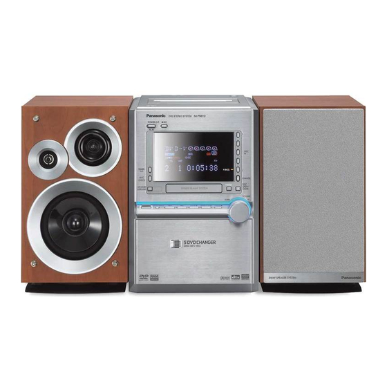
SA-PM91DEE
Colour
(S) ... Silver Type
10. MP3/WMA*
40 W per channel (6Ω)
40 W per channel (6Ω)
11. JPEG*
160 W
35 W per channel (6Ω)
35 W per channel (6Ω)
12. HighMAT Level 2 (Audio and Image)
140 W per channel
13. HDCD
Stereo, 3.5 mm jack
* The total combined maximum number of recognizable audio and
picture contents and groups: 4000 audio and picture contents and
400 groups.
Audio output
Number of channels
Digital audio output
Optical digital output
Pick up
Wavelength
DVD
CD
Laser power
n Video Section
Video system
DVD Stereo System
· Compatible compression rates:
MP3: between 32 kbps and 320 kbps
WMA: between 48 kbps and 320 kbps
· Exif Ver 2.1 JPEG Baseline files
· Picture resolution:
between 320 x 240 and 6144 x 4096 pixels
(Sub sampling is 4:2:2 or 4:2:0)
© 2005 Matsushita Electric Industrial Co. Ltd.. All
rights
reserved.
distribution is a violation of law.
ORDER NO. MD0504152C3
Optical terminal
662 nm
785 nm
CLASS 2/CLASS 3a
PAL625/50, PAL525/60, NTSC
Unauthorized
copying
and
2
Advertisement
Table of Contents

Related Manuals for Panasonic SA-PM91DEE


Summary of Contents for Panasonic SA-PM91DEE
- Page 1 ORDER NO. MD0504152C3 DVD Stereo System SA-PM91DEE Colour (S) ... Silver Type Specification n Amplifier Section 10. MP3/WMA* · Compatible compression rates: RMS Output Power Stereo mode (Both channel driven) 10% total harmonic distortion MP3: between 32 kbps and 320 kbps 1 kHz, (Low channel) 40 W per channel (6Ω)
-
Page 2: Table Of Contents
4.8 cm/sec Overall frequency response (+3, -6 dB) at Deck Out n System Normal 35 Hz - 14 kHz n System: SC-PM91DEE-S Music Center: SA-PM91DEE-S S/N ratio 50 dB (A weighted) Speaker: SB-PM91P-MJ Wow and flutter 0.18% (WRMS) Notes : Fast forward and rewind time Approx. - Page 3 SA-PM91DEE 12.6. Disassembly of Panel P.C.B 15.4. Using Recovery Disc 12.7. Disassembly of Switch P.C.B 15.5. Total Usage Time Display 12.8. Disassembly of Rear Cabinet 16 Procedure for Checking Operation of Individual Parts for 12.9. Disassembly of Tuner Pack Deck Mechanism Unit 12.10.
-
Page 4: Safety Precautions
SA-PM91DEE 1 Safety Precautions 1.1. GENERAL GUIDELINES 1. When servicing, observe the original lead dress. If a short circuit is found, replace all parts which have been overheated or damaged by the short circuit. 2. After servicing, ensure that all the protective devices such as insulation barriers, insulation papers shields are properly installed. -
Page 5: Before Repair And Adjustment
SA-PM91DEE 2 Before Repair and Adjustment Disconnect AC power, discharge Power Supply Capacitors C5802, C5803, C5804, C5912, C5902, C5901, C5916, C5915, C5905, C5904, C2843 and C2824 through a 10 Ω, 1 W resistor to ground. DO NOT SHORT-CIRCUIT DIRECTLY (with a screwdriver blade, for instance), as this may destroy solid state devices. -
Page 6: Handling The Lead-Free Solder
SA-PM91DEE 5 Handling the Lead-free Solder 5.1. About lead free solder (PbF) Distinction of PbF P.C.B.: P.C.B.s (manufactured) using lead free solder will have a PbF stamp on the P.C.B. Caution: · Pb free solder has a higher melting point than standard solder; Typically the melting point is 50 - 70°F (30 - 40°C) higher. Please use a high temperature soldering iron. -
Page 7: Precaution Of Laser Diode
SA-PM91DEE 6 Precaution of Laser Diode CAUTION: This unit utilizes a class 1 laser. Invisible laser radiation is emitted from the optical pickup lens. When the unit is turned on: 1. Do not look directly into the pick up lens. -
Page 8: Cautions To Be Taken When Handling Optical Pickup
SA-PM91DEE 7 Cautions to be taken when handling Optical Pickup The laser diode used inside optical pickup could be destroyed due to static electricity as a potential difference is caused by electrostatic load discharged from clothes or human body. Handling the parts carefully to avoid electrostatic destruction during repair. -
Page 9: Accessories
SA-PM91DEE 8 Accessories Note : Refer to Packaging Materials & Accessories Part List (Section 26.5) for part number. Remote Control AC Cord FM Antenna AM Loop Antenna Video Cable... -
Page 10: Operation Procedures
SA-PM91DEE 9 Operation Procedures... - Page 11 SA-PM91DEE...
-
Page 12: Disc Information
SA-PM91DEE 10 Disc Information... - Page 13 SA-PM91DEE...
-
Page 14: About Highmat
SA-PM91DEE 11 About HighMAT 11.1. What’s HighMAT? Consumers worldwide are using PCs to create their own collections of music, photos and even video by burning them onto CDs. But how these collections can be experienced across different devices can be confusing to navigate, time consuming to access for a DVD player, and be incomplete in terms of music information available to the customer. -
Page 15: Benefits Of Highmat
SA-PM91DEE A Solution Created: HighMAT delivers a better digital media access experience by creating a standard approach for PCs to structure digital media on various physical formats and for playback devices to read the data. 11.3. Benefits of HighMAT? Conventional... - Page 16 SA-PM91DEE...
- Page 17 SA-PM91DEE HighMAT is now available for CD Burning and in Leading DVD PlayersHighMAT is a new technology that is now available in leading software and consumer electronic devices to dramatically improve the digital media experience when you create homemade CDsHighMAT delivers a simple, standardized way for PC software and consumer electronics devices to talk to each other and work better together.
-
Page 18: Assembling And Disassembling
SA-PM91DEE 12 Assembling and Disassembling. “ATTENTION SERVICER” Some chassis components maybe have sharp edges. Be careful when disassembling and servicing. 1. This section describes procedures for checking the operation of the major printed circuit boards and replacing the main components. -
Page 19: Disassembly Flow Chart
SA-PM91DEE 12.1. Disassembly flow chart The following chart is the procedure for disassembling the casing and inside parts for internal inspection when carrying out the servicing. To assemble the unit, reverse the steps shown in the chart below. -
Page 20: Disassembly Of Side Panel (L) & (R)
SA-PM91DEE 12.2. Disassembly of Side Panel (L) & (R) Step 1 : Release catches at both ends. Step 2 : Lift up the top cabinet unit, push backward as arrow shown and flip top cabinet unit sideway. Step 1 : Remove 5 screws. -
Page 21: Disassembly Of Front Panel Assembly
SA-PM91DEE Step 1 : Detach the FFC CN2805. Step 1 : Remove 1 screw. Step 2 : Release the clutch. Step 2 : Detach the connector CN5901. Step 3 : Remove 4 screws. Step 4 : Push the lever as arrow shown to open the cassette lid and remove the deck mechanism unit. -
Page 22: Disassembly Of Switch P.c.b
SA-PM91DEE · Follow the (Step 1) - (Step 4) of Item 12.3. · Follow the (Step 1) - (Step 4) of Item 12.5. Step 4 : Detach the connector CN603. 12.7. Disassembly of Switch P.C.B Step 1 : Remove 6 screws. -
Page 23: Disassembly Of Rear Cabinet
SA-PM91DEE 12.8. Disassembly of Rear Cabinet · Follow the (Step 1) - (Step 6) of Item 12.2. · Follow the (Step 1) - (Step 4) of Item 12.3. Step 2 : Release 6 catches. Step 1 : Remove 14 screws. -
Page 24: Disassembly Of Harmonic Bass P.c.b
SA-PM91DEE · Follow the (Step 1) - (Step 4) of Item 12.3. 12.10. Disassembly of Harmonic · Follow the (Step 1) - (Step 4) of Item 12.8. Bass P.C.B · Follow the (Step 1) - (Step 6) of Item 12.2. -
Page 25: Disassembly Of Transformer P.c.b
SA-PM91DEE Step 1 : Detach the FFC CN2806. Step 1 : Detach the connector CN5801, CN5901. Step 2 : Detach the FFC CN2805 and connection CN2801, CN2802. Step 2 : Remove 4 screws. 12.15. Disassembly of Power P.C.B · Follow the (Step 1) - (Step 6) of Item 12.2. -
Page 26: Disassembly Of Dvd Mechanism Unit
SA-PM91DEE Step 3 : Remove the Power P.C.B as arrow shown. 12.16. Disassembly of DVD Mechanism Unit · Follow the (Step 1) - (Step 6) of Item 12.2. · Follow the (Step 1) - (Step 4) of Item 12.3. · Follow the (Step 1) - (Step 4) of Item 12.5. -
Page 27: Procedure For Replacing Deck Holder
SA-PM91DEE Step 1 : Remove 1 screw and lift up damper gear. Step 2 : Remove the cassette open spring. Step 1 Remove 2 screws. Step 2 Unsolder the terminals of Power Amp IC (IC500) and replace the component. 12.18. Procedure for Replacing Deck Step 3 : Pull out the ribs of the cassette holder to the arrow direction. -
Page 28: Procedure For Replacing Pinch Roller And Head Block (Deck Mechanism Unit)
SA-PM91DEE Step 2 : Push the spring as arrow shown. Step 3 : Remove the CD lid as arrow shown. 12.20. Procedure for Replacing Pinch Roller and Head Block (Deck Mechanism Unit) · Follow the (Step 1) - (Step 6) of Item 12.2. -
Page 29: Procedure For Replacing Motor, Capstan Belt A, Capstan Belt B, And Winding Belt (Deck Mechanism Unit)
SA-PM91DEE 12.21. Procedure for Replacing Motor, Capstan Belt A, Capstan Belt B, and Winding Belt (Deck Mechanism Unit) · Follow the (Step 1) - (Step 6) of Item 12.2. · Follow the (Step 1) - (Step 4) of Item 12.3. -
Page 30: Procedure For Replacing Parts On Deck Mechanism Pcb
SA-PM91DEE 12.22. Procedure for Replacing Parts on Deck Mechanism PCB · Follow the (Step 1) - (Step 6) of Item 12.2. · Follow the (Step 1) - (Step 4) of Item 12.3. · Follow the (Step 1) - (Step 4) of Item 12.4. -
Page 31: Cr16 Mechanism Disassembly Procedure
SA-PM91DEE 2. Unplug AC power cord after the indication of [BYE], then disassemble the body. 3. Disassemble the body, and take out CD loading mechanism. 4. Perform disassembly according to the following procedure for disassembly. 12.24. CR16 mechanism disassembly procedure 12.24.1. - Page 32 SA-PM91DEE...
- Page 33 SA-PM91DEE...
- Page 34 SA-PM91DEE 12.24.4. Disassembly of Traverse Motor (Unit) and Spindle Motor (Unit) · Follow the (Step 1) - (Step 6) of Item 12.2. · Follow the (Step 1) - (Step 4) of Item 12.3. · Follow the (Step 1) - (Step 4) of Item 12.5.
- Page 35 SA-PM91DEE 12.24.5. Replacement for the disc tray · Follow the (Step 1) - (Step 6) of Item 12.2. · Follow the (Step 1) - (Step 4) of Item 12.3. · Follow the (Step 1) - (Step 4) of Item 12.5.
- Page 36 SA-PM91DEE...
- Page 37 SA-PM91DEE 12.24.6. Replacement for the traverse deck · Follow the (Step 1) - (Step 6) of Item 12.2. · Follow the (Step 1) - (Step 4) of Item 12.3. · Follow the (Step 1) - (Step 4) of Item 12.5.
- Page 38 SA-PM91DEE 12.24.7. Disassembly for loading unit · Follow the (Step 1) - (Step 6) of Item 12.2. · Follow the (Step 1) - (Step 4) of Item 12.3. · Follow the (Step 1) - (Step 4) of Item 12.5. · Follow the (Step 1) - (Step 4) of Item 12.8.
- Page 39 SA-PM91DEE...
- Page 40 SA-PM91DEE...
-
Page 41: Cr16 Mechanism Assembly Procedure
SA-PM91DEE 12.25. CR16 MECHANISM ASSEMBLY PROCEDURE The following specified greases and/or oil must be applied when some specific parts are changed. 1. Floil grease (VFK1298) : The floil grease must be applied to tray, tray (L) and tray (R). 2. Hanarl oil (VFK1700) : The hanarl oil must be applied to any parts with grease other than the said parts. - Page 42 SA-PM91DEE...
- Page 43 SA-PM91DEE...
- Page 44 SA-PM91DEE...
- Page 45 SA-PM91DEE...
- Page 46 SA-PM91DEE...
- Page 47 SA-PM91DEE...
- Page 48 SA-PM91DEE...
- Page 49 SA-PM91DEE...
- Page 50 SA-PM91DEE...
- Page 51 SA-PM91DEE...
- Page 52 SA-PM91DEE...
-
Page 53: Disassembly Of Traverse Mechanism
SA-PM91DEE 12.26. Disassembly of traverse mechanism · Follow the (Step 1) - (Step 6) of Item 12.2. · Follow the (Step 1) - (Step 4) of Item 12.3. · Follow the (Step 1) - (Step 4) of Item 12.5. · Follow the (Step 1) - (Step 4) of Item 12.8. -
Page 54: Handling Of Cassette Tape Jam
SA-PM91DEE 12.27. Handling of cassette tape jam · Follow the (Step 1) - (Step 6) of Item 12.2. -
Page 55: Service Positions
SA-PM91DEE 13 Service Positions 13.1. Checking procedure Note: For the disassembling procedure, see the section 12. 13.2. Checking the major P.C.B. 1. Disassembly of Side Panel L & R 9. Disassembly of Harmonic Bass P.C.B. 2. Disassembly of Top Cabinet 10. -
Page 56: Self-Diagnosis Function
SA-PM91DEE 14 Self-Diagnosis Function This unit is equipped with the self-diagnosis function, which displays an error when it occurs, for use during servicing. 14.1. Automatic Displayed Error Codes 14.1.1. Automatic Display Function For a power unit error, the code is automatically displayed. -
Page 57: Opecon Version And Eeprom Checksum Display
SA-PM91DEE Fig. 14-2 14.2.2. Re-Display · Press the power button to turn off the power, and then turn on the power. · The details of self diagnosis are stored in the unit memory. To retrieve them, follow the procedure described the above, “Activating Self-Diagnosis Function and Displaying Method”. -
Page 58: Self-Diagnosis Error Code Description
SA-PM91DEE 14.5. Self-Diagnosis Error Code Description Code Display Abnormal Item Detection Method Abnormal output or power supply When DCDET becomes L while operating, PCONT is set to L without usual POWER OFF processing, and F61 is displayed after GOOD-BYE display. -
Page 59: Service Mode Table
SA-PM91DEE Abnormal display The error is detailed F506 Media cannot distinguish. (It is invalid media.) F600 Administrative information cannot be acquired by the recovery error. F601 Irregular sector ID demand F602 LEAD-IN information cannot be acquired by the recovery error. - Page 60 SA-PM91DEE Item Operational Condition Details Display To Exit Mode and Key Function Measurement of CD While the player is Measurement of CD laser current [xxx_yyy_DC] Automatically exits laser current stopped and no disc is electricity the mode after five electricity...
-
Page 61: Tray Lock Function
SA-PM91DEE Item Operational Condition Details Display To Exit Mode and Key Function Laser use time While the player is Laser usage time [_1234_5678] Automatically exits stopped and no disc is Measures each for DVD and CD the mode after five... -
Page 62: Things To Do After Repair (Precaution)
SA-PM91DEE [OPEN/CLOSE] · Operation Lock Function 1. With the SELECTOR on DVD/CD and POWER ON, hold down the [DVD/CD] KEY on the main unit, and then press the [POWER] KEY on the remote control for 3 seconds to enter Lock mode B. -
Page 63: Error Detection Code For Cassette Mechanism Block
SA-PM91DEE Error Code Abnormal Items Possible Cause CD power abnormal under normal operation (self-diagnostic mode inclusive), check if CDRST is H for SELECTOR at CD. If it is not H after 1 sec, it shall be memorised as an error. -
Page 64: Changer Reliability Test 3
SA-PM91DEE Ageing process: Operation Tray 1 CLOSE READ OPEN CLOSE CHANGE Tray 2 CLOSE READ OPEN CLOSE CHANGE Tray 3 CLOSE READ OPEN CLOSE CHANGE Tray 4 CLOSE READ OPEN CLOSE CHANGE Tray 5 CLOSE READ OPEN CLOSE CHANGE (Back to tray 1 and repeat) Note: To exit ageing mode, press [POWER] button. - Page 65 SA-PM91DEE Display Example: [1OP000000] ...TRAY OPEN [1CL000000] ...TRAY CLOSE [1CH000000] ...TRAY CHANGING...
-
Page 66: Cautions To Be Taken During Servicing
SA-PM91DEE 15 Cautions To Be Taken During Servicing 15.1. Recovery after the dvd player is repaired · When Flash ROM or DVD Module P.C.B. is replaced, carry out the recovery processing to optimize the drive. Playback the recovery disc to process the recovery automatically. -
Page 67: Using Recovery Disc
SA-PM91DEE 15.4. Using Recovery Disc 15.4.1. Recovery Process 1. Insert the recovery disc (RFKZD03R005) to the player to replay. 2. The recovery process automatically starts, and a message of completion prompts on the screen. 3. Remove the disc. 4. Turn off the power. -
Page 68: Procedure For Checking Operation Of Individual Parts For Deck Mechanism Unit
SA-PM91DEE 16 Procedure for Checking Operation of Individual Parts for Deck Mechanism Unit 16.1. Operation Check with Cassette Tape 1. Pull up the EJECT lever using a rubber band. (Fig. 6) 2. Supply DC5V to MOTOR. (→ MOTOR rotates.) (Fig. 5) 3. - Page 69 SA-PM91DEE...
-
Page 70: Measurement And Adjustments
SA-PM91DEE 17 Measurement And Adjustments 17.1. Cassette Deck Section 17.1.1. Requirements · Test tape (QZZCFM) (QZZCWAT) · Normal blank cassette tape (QZZCRA) · Digital frequency counter · Oscilloscope · Electrical voltmeter · Headphone jack output jig (Fig. 8) 17.1.2. Setting of Unit ·... - Page 71 SA-PM91DEE Fig. 10 Fig. 11 17.1.5. Bias Voltage Check 1. Connect an electrical voltmeter. (Fig. 12) 2. Set the function to “TAPE” position. 3. Insert a normal blank cassette tape (QZZCRA). 4. While pressing and holding down [ REC] button, press [TAPE ] button to pause the recording mode.
-
Page 72: Voltage Measurement And Waveform Chart
SA-PM91DEE 18 Voltage Measurement and Waveform Chart Note: · Indicated voltage values are the standard values for the unit measured by the DC electronic circuit tester (high-impedance) with the chassis taken as standard. Therefore, there may exist some errors in the voltage values, depending on the internal impedance of the DC circuit tester. - Page 73 SA-PM91DEE Ref No. IC8051 MODE CD PLAY STANDBY IC8051 Ref No. MODE CD PLAY STANDBY IC8051 Ref No. MODE CD PLAY STANDBY IC8111 Ref No. MODE CD PLAY STANDBY Ref No. IC8251 MODE CD PLAY STANDBY IC8251 Ref No. MODE...
- Page 74 SA-PM91DEE 18.1.3. Main P.C.B. MAIN P.C.B. IC2801 Ref No. MODE CD PLAY STANDBY IC2801 Ref No. MODE CD PLAY STANDBY IC2801 Ref No. MODE CD PLAY STANDBY IC2801 Ref No. MODE CD PLAY STANDBY IC2801 Ref No. MODE CD PLAY...
- Page 75 SA-PM91DEE IC2808 Ref No. MODE CD PLAY STANDBY IC2808 Ref No. MODE CD PLAY STANDBY Ref No. IC2809 MODE CD PLAY STANDBY -0.1 IC2810 Ref No. MODE CD PLAY STANDBY IC2811 Ref No. MODE CD PLAY STANDBY IC2812 Ref No.
- Page 76 SA-PM91DEE 18.1.5. Panel P.C.B. PANEL P.C.B. Ref No. IC601 MODE CD PLAY -29.5 -29.4 -29.4 -29.5 -27.5 -31.4 -23.4 -25.4 -23.4 -31.6 STANDBY IC601 Ref No. MODE -29.5 -27.5 CD PLAY -25.4 -29.5 -27.5 -31.7 -25.5 -23.3 -23.4 -29.6 -25.4 -29.5...
- Page 77 SA-PM91DEE 18.1.9. Power P.C.B. POWER P.C.B. IC500 Ref No. MODE CD PLAY -34.5 34.2 34.2 -34.5 -15.1 34.2 -34.5 STANDBY -0.4 -0.4 -0.4 -0.4 Ref No. Q5101 Q5102 Q5201 Q5202 Q5801 MODE CD PLAY -0.8 -0.1 -0.9 -0.2 -0.8 -0.1 -0.9...
-
Page 78: Waveform
SA-PM91DEE 18.2. Waveform CN2801 PIN 1 CN2801 PIN 8 CN2803 PIN 1 CN2803 PIN 2 CD PLAY CD PLAY CD PLAY CD PLAY 1.18Vp-p (10msec.div) 5.28Vp-p (10msec.div) 5.24Vp-p (10msec.div) 4.20Vp-p (10msec.div) CN2803 PIN 3 CN2803 PIN 21 CN2805 PIN 10... -
Page 79: Block Diagram
SA-PM91DEE 19 Block Diagram 19.1. DVD Module Block OPTICAL PICKUP LD(DVD) SPINDLE MOTOR UNIT LD(CD) Q8552 Q8562 SWITCH SWITCH BIAS1 IC8251 C0GBG0000048 OPIN+ MOTOR DRIVE LDIN BIAS2 Q8551 Q8561 TRIN SWITCH SWITCH QR8571 SUPPLY SWITCH CONTROL 130 134 129 133 127 110 111 132 131 136 115 135 114 137 116 138 117 DV2.1... - Page 80 SA-PM91DEE Q8550 SWITCH Q8560 SWITCH IC8601 C0EBE0000384 D8550 RESET IC IC8051 IC8651 C3ABPG000133 XRESET RFKWMH82H160 64 SDRAM 16M FLASH ROM Q8607 SWITCH 2,4,5,7,8,10,11, 22-26, 9,10,16,17,48 1-8,18-25 39-36, 38-45 13,42,44,45,47, 29-35 Q8606 48,50,51,53 SWITCH IC8606 C0EBA0000031 RESET IC IC8611 C3EBGC000044 16M EEPROM IC...
- Page 81 SA-PM91DEE TO MAIN BLOCK QR8111 SWITCH QR8112 SWITCH 15(14) 10(9) IC8111 C0CBCBD00018 3.3V REGULATOR IC8420 C0FBBK000049 AUDIO DAC IC8695 IC8691 C0JBAA000346 C0JBAA000346 LOGIC IC LOGIC IC QR8420 MUTING SWITCH TO MAIN BLOCK 169 171 170 163 149 151 152 156 158 DV2.1...
-
Page 82: Main Block
SA-PM91DEE 19.2. Main Block (DECK 2) FILTER R/P HEAD IC1001 AN7326K P/B REC AMP 22(1) 21(2) 20(3) 19(4) 16(7) 15(8) RIPPLE REJECTION LOGIC SWITCH REC AMP (L) MUTE Q1101 IC1000 (Q1201) C1AA00000612 ANALOG SWITCH MUTING SWITCH Q1302 Q1317 DECK BEAT PROOF... - Page 83 SA-PM91DEE JK2805 SCART TERMINAL C_OUT BLUEIN CBOUT MIX_L(R) CBSAG Y_OUT GREENIN CYOUT CYSAG Y/PY/G COUT CYIN IC2809 IC2808 REDIN_CIN C1AB00001731 C9ZB00000431 VIDEO BUFFER IC CROUT VIDEO IC CB/PB/B CRSAG CBIN JK2802 VIDEO OUT VOUT VSAG MUTE2 IC2810 VOUT_YIN C1AB00001731 VIDEO BUFFER IC...
- Page 84 SA-PM91DEE FL601 FROM POWER 51,54 1G, 4G FL DISPLAY TRANSFORMER 50~84 55~66 Q601, Q602 DRIVER 16~23, 25~51 53~64 DIG00,DOG03 IC601 C0HBB0000039 Q2827 FL DRIVER 11,52 REGULATOR VCC1,2 IC2805,IC2806,IC2807 C0DBEFG00003 C0DBZHG00016 C0DBZHE00019 REGULATOR RM11 RM21 UP/DOWN MOTOR LOADING MOTOR IC2803,IC2804 IC2811...
- Page 85 SA-PM91DEE 4(3) 1(2) 12(13) 6(7) MIXL(R) IC2812 C1BB00000822 ASP IC FILTER IC2814 10(11) 8(9) 24(23) KIA4558FEL IC2817 DUAL OP-AMP C0ABBB000067 DUAL OP-AMP JK2801 FILTER IC2813 IC2818 C0AABB000085 C0ABBB000067 DUAL OP-AMP DUAL OP-AMP 2(6) 2(6) 1(7) 1(7) 3(5) 3(5) FILTER Q2101...
- Page 86 SA-PM91DEE Q2810 LEVEL SWITCH Q2811 LEVEL SWITCH JK2800 SUBWOOFER Q2816 MUTE SWITCH Q2205 (Q2204) Q2102 LEVEL MOTOR (Q2202) SWITCH SWITCH DRIVER JK2804 SUPPLY HEADPHONE Q2806~ Q2809 Q2103(Q2203) Q2812 SWITCH SWITCH Q611 S1901 DC DETECT TAPE EJECT SWITCH Q5809,Q5808 SWITCH IC2801...
- Page 87 SA-PM91DEE IC500 RSN315H41-P POWER HIC 16(15) 13(12) 5(7) 1(4) D5818 Q5101 (Q5201) FILTER AMPLIFIER HI_L(R) JK1000, JK1001 Q5102 (Q5202) FILTER AMPLIFIER LO_L(R) Q5810 D5819 SWITCH Q5903 SWITCH Q5806 Q5904 D5909~D5912 SWITCH D5917 SWITCH T5901 Q5801 D5801 SUB+B REGULATOR FP5801 Q5807...
-
Page 88: Notes Of Schematic Diagram
SA-PM91DEE 20 Notes of Schematic Diagram (All schematic diagrams may be modified at any time with the development of new technology) Note : Stock switch Play switch Bottom switch Open switch Change switch S601 Bass/Treble switch S602 REW switch S603... -
Page 89: Schematic Diagram
SA-PM91DEE 21 Schematic Diagram 21.1. Optical Pickup Unit Circuit SCHEMATIC DIAGRAM - 1 OPTICAL PICKUP UNIT CIRCUIT : +B SIGNAL LINE : CD-DA SIGNAL LINE J0JBC0000105 J0JBC0000105 TO ACT GND (IM) MODULE VREF2(RF-) CIRCUIT PIN (DVD) (FP8501) ON LD (CD) -
Page 90: Dvd Module Circuit
SA-PM91DEE 21.2. DVD Module Circuit SCHEMATIC DIAGRAM - 2 DVD MODULE CIRCUIT : +B SIGNAL LINE : CD-DA SIGNAL LINE TRV-I-SW D+5V FODRV TRDRV C8251 6.3V220 R8265 TL8201 VHALF C8262 R8201 C8261 2.2K PNRST LDCNT BIAS1 MUTE3 VIN1 MUTE3 R8241... - Page 91 SA-PM91DEE SCHEMATIC DIAGRAM - 3 DVD MODULE CIRCUIT : +B SIGNAL LINE D+3.3V IC8111 C0CBCBD00018 3.3 REGULATOR IC TL8111 D+5V C8111 C8112 R8112 R8111 IC8111 C8113 QR8112 470P QR8111 Cont UNR521400L UNR521400L SWITCH SWITCH D+1.2V QR8571 B1GDCFEC0001 CL8571 SUPPLY CONTROL SWITCH...
- Page 92 SA-PM91DEE SCHEMATIC DIAGRAM - 4 : MAIN SIGNAL LINE : DVD VIDEO SIGNAL LINE DVD MODULE CIRCUIT : +B SIGNAL LINE FP8101 CKC1 VGND Y/PY/G Y/PY/G LB8303 J0JCC0000119 CKC2 VGND CB/PB/B CB/PB/B LB8304 J0JCC0000119 CKC4 VGND CR/PR/R CR/PR/R LB8305 J0JCC0000119...
- Page 93 SA-PM91DEE SCHEMATIC DIAGRAM - 5 DVD MODULE CIRCUIT : +B SIGNAL LINE IC8651 RFKWMH82H160 16M FLASH ROM IC EXADT15 EXADR16 EXADT14 XBYTE EXADT13 EXADT12 FDT15 DQ15/A-1 EXADT11 FDT7 EXADT10 FDT14 DQ14 EXADT9 FDT6 EXADT8 FDT13 DQ13 EXADR19 FDT5 EXADR20 FDT12...
- Page 94 SA-PM91DEE SCHEMATIC DIAGRAM - 6 DVD MODULE CIRCUIT : +B SIGNAL LINE C8028 C8027 C8026 C8024 C8023 C8051 2200P MDQ0 MDQ15 DQ15 C8052 VDDQ VSSQ MDQ1 MDQ14 DQ14 C8025 C8022 MDQ2 MDQ13 DQ13 C8057 2200P RX8013 VSSQ VDDQ (82 x 4)
- Page 95 SA-PM91DEE SCHEMATIC DIAGRAM - 7 DVD MODULE CIRCUIT : +B SIGNAL LINE RX8018 (82 x 4) RX8017 RX8014 (82 x 4) C8021 (82 x 4) RX8015 (22 x 2) MDQ9 MDQ24 MDQ5 VDD33 MDQ10 TRCST MDQ4 TRCDATA3 VDD33 TRCDATA2 MDQ11...
- Page 96 SA-PM91DEE SCHEMATIC DIAGRAM - 8 : CD-DA SIGNAL LINE : DVD VIDEO SIGNAL LINE DVD MODULE CIRCUIT : +B SIGNAL LINE : DVD AUDIO SIGNAL LINE LB8001 CKB9 J0JHC0000045 D+3.3V D+1.2V C8002 C8001 LB8002 4V330 6.3V100 J0JHC0000045 CKA2 C8017 RX8031 CKA7 (4.7K x 2)
-
Page 97: Main Circuit
SA-PM91DEE 21.3. Main Circuit SCHEMATIC DIAGRAM-9 : DVD (VIDEO) SIGNAL LINE : AUX SIGNAL LINE MAIN CIRCUIT : FM/AM SIGNAL LINE : +B SIGNAL LINE R2050 R2203 VREF+ R2861 AUXR R2860 C2204 R2204 R2859 1000P C2811 100P TAPE_EJECT C2813 470P... - Page 98 SA-PM91DEE SCHEMATIC DIAGRAM-10 MAIN CIRCUIT : DVD (VIDEO) SIGNAL LINE : +B SIGNAL LINE IC2807 C2810 C0DBZHE00019 100P REGULATOR IC R2015 R2843 100K R2016 100K R2858 D+1.2V C2998 D+5V A+5V C2861 C2864 C2862 C2863 16V47 16V470 DVDPCONT R2842 SC_WIDE ASP_CLK...
- Page 99 SA-PM91DEE SCHEMATIC DIAGRAM-11 : DVD (VIDEO) SIGNAL LINE : - B SIGNAL LINE : MAIN SIGNAL LINE MAIN CIRCUIT : +B SIGNAL LINE MUTE_H IC2805 IC2806 C0DBEFG00003 OP_LEV C0DBZHG00016 REGULATOR IC DCDET REGULATOR IC PCONT L2807 L2806 G0A200D00002 G0A101ZA0028 SYNC...
- Page 100 SA-PM91DEE : TAPE PLAYBACK SIGNAL LINE SCHEMATIC DIAGRAM-12 : MAIN SIGNAL LINE : TAPE RECORD SIGNAL LINE : - B SIGNAL LINE : FM/AM SIGNAL LINE : AUX SIGNAL LINE MAIN CIRCUIT : +B SIGNAL LINE L2101, L2201 J0JBC0000019 HP_SW...
- Page 101 SA-PM91DEE : TAPE PLAYBACK SIGNAL LINE SCHEMATIC DIAGRAM-13 : TAPE RECORD SIGNAL LINE : MAIN SIGNAL LINE : - B SIGNAL LINE : DVD (AUDIO) SIGNAL LINE MAIN CIRCUIT : +B SIGNAL LINE : DVD (VIDEO) SIGNAL LINE C2932 0.082...
-
Page 102: Panel Circuit, Harmonic Bass Circuit & Switch Circuit
SA-PM91DEE 21.4. Panel Circuit, Harmonic Bass Circuit & Switch Circuit SCHEMATIC DIAGRAM - 14 : -B SIGNAL LINE PANEL CIRCUIT : +B SIGNAL LINE 86 85 84 83 82 81 80 79 78 77 76 75 74 73 72 71 70 69 68 67 66 65 64 63 62 61 60 59 58 57 56 55 54 53 52 51 50 49 48 47... - Page 103 SA-PM91DEE SCHEMATIC DIAGRAM - 15 : MAIN SIGNAL LINE : +B SIGNAL LINE : -B SIGNAL LINE PANEL CIRCUIT HARMONIC BASS CIRCUIT R3129 R3124 C3000 C3002 R3139 C3010 220P 50V1 C3007 R3126 4.7K R3117 50V2.2 220P R3102 R3125 L_IN SGND...
-
Page 104: Scart Terminal Circuit & Speaker Circuit
SA-PM91DEE 21.5. Scart Terminal Circuit & Speaker Circuit SCHEMATIC DIAGRAM-16 : MAIN SIGNAL LINE : +B SIGNAL LINE : DVD (VIDEO) SIGNAL LINE SCART TERMINAL CIRCUIT Q2821 Q2822 KTC3199GRTA KTC3205YTA SWITCH SWITCH R2984 AUDIOOUT(B) Q2819 AUDIOIN(B) R2990 L2826, L2827 UNR211500L... -
Page 105: Transformer Circuit
SA-PM91DEE 21.6. Transformer Circuit SCHEMATIC DIAGRAM-17 : -B SIGNAL LINE : +B SIGNAL LINE TRANSFORMER CIRCUIT D5917 R5914 R5913 R5912 B0EAKM000117 Q5904 2SD21370PA R5908 REGULATOR C5909 C5914 0.01 0.01 R5911 C5915 50V47 Q5903 C5907 R5906 50V4.7 C5906 D5908 B0AACK000004 RL5901... -
Page 106: Power Circuit
SA-PM91DEE 21.7. Power Circuit SCHEMATIC DIAGRAM-18 : -B SIGNAL LINE POWER CIRCUIT : +B SIGNAL LINE : MAIN SIGNAL LINE IC500 IC500 RSN315H41-P POWER AMP HIC R5153 Q5101,Q5201 4.7K KTC3199GRTA SWITCH C5817 C5153 R5151 0.01 3.9K 50V0.22 C5151 R5209 C5205... - Page 107 SA-PM91DEE SCHEMATIC DIAGRAM-19 : -B SIGNAL LINE POWER CIRCUIT : +B SIGNAL LINE : MAIN SIGNAL LINE LO_R LO_L LO_R_GND SPEAKER LO_L_GND CIRCUIT HI_R_GND (CN5805) ON HI_L_GND SCHEMATIC HI_R DIAGRAM-16 HI_L H5804 R5210 100K R5258 R5834 R5830 R5158 R5110 R5259...
-
Page 108: Deck Circuit, Tape Eject Circuit & Deck Mechanism Circuit
SA-PM91DEE 21.8. Deck Circuit, Tape Eject Circuit & Deck Mechanism Circuit SCHEMATIC DIAGRAM-20 : TAPE PLAYBACK SIGNAL LINE DECK CIRCUIT : +B SIGNAL LINE : TAPE RECORD SIGNAL LINE C1105 470P R1103 C1122 0.01 R1101 C1104 0.027 C1102 C1101 1000P... - Page 109 SA-PM91DEE SCHEMATIC DIAGRAM-21 : TAPE PLAYBACK SIGNAL LINE DECK CIRCUIT : +B SIGNAL LINE : TAPE RECORD SIGNAL LINE R1105 R1109 2.2K R1107 Q1101 C1110 R1106 0.0068 100K Q1101,Q1201 2SD2114K1V R1205 MUTING SWITCH R1209 2.2K R1207 Q1201 R1206 C1210 100K 0.0068...
-
Page 110: Cd Loading Circuit
SA-PM91DEE 21.9. CD Loading Circuit SCHEMATIC DIAGRAM-22 CD LOADING CIRCUIT : +B SIGNAL LINE IC11 C0GAG0000007 UP/DOWN MOTOR DRIVE 0.01 16V100P RM11 UP/DOWN MOTOR CHANGE BOTTOM OPEN B3NAA0000098 +7.5V SENSOR STOCK PGND CR16 SWITCH DGND UP/DOWN F PLAY UP/DOWN R... -
Page 111: Printed Circuit Board
SA-PM91DEE 22 Printed Circuit Board 22.1. DVD Module P.C.B. (Side: A & B) DVD MODULE P.C.B (REPV0057B) FP8501 TO OPTICAL PICKUP UNIT R8263 23 21 C8262 C8255 R8261 C8257 C8252 C8251 Q8552 Q8562 R8554 C8554 R8558 IC8606 R8553 R8565 R8564... - Page 112 SA-PM91DEE DVD MODULE P.C.B (REPV0057B) CKE24 C8503 LB8502 CKE6 CKE11 CKE12 CKE25 CKE19 CKE14 IC8251 CKE2 CKE22 CKE9 CKE3 C8502 CKE13 CKE23 RX8502 RX8504 CKE7 CKE5 RX8501 RX8503 C8506 LB8514 D8550 R8569 C8261 C8254 Q8560 LB8507 TL8513 R8262 R8264 CKE4...
-
Page 113: Main P.c.b
SA-PM91DEE 22.2. Main P.C.B. MAIN P.C.B (REPV0054E) CN2808 Q2808 Q2807 TO FAN W2144 C2806 R2841 C2810 W2145 R2840 R2838 Q2806 C2927 R2837 R2015 C2888 R2853 R2831 R2847 R2856 C2890 C2894 D2811 R2007 W2035 R2828 R2900 R2929 R2920 C2813 R2821 Q2809... - Page 114 SA-PM91DEE PHONE 6-SW CN2808 JK2804 Q2808 Q2807 TO FAN Q2806 C2888 C2101 C2894 C2890 D2811 C2201 R2900 R2920 R2929 Q2809 CN2804 TUNER PACK (ENG07808QF) C2104 W2093 JK2801 C2900 R2931 R2105 C2903 C2902 W2226 C2858 R2205 R2907 C2857 C2895 W2162 C2852...
-
Page 115: Panel P.c.b
SA-PM91DEE 22.3. Panel P.C.B. PANEL P.C.B (REPV0053A) R643 C633 C622 C621 D616 S616 R612 S617 POWER C630 S618 DISC 1 R613 E601 FL601 46 47 52 53 54 55 56 57 58 59 60 61 62 63 64 65 80 81... -
Page 116: Transformer P.c.b
SA-PM91DEE 22.4. Transformer P.C.B. TRANSFORMER P.C.B (REPV0052A) 250V 800mA T5902 SUB-TRANSFORMER RL5901 W1001 W1002 T5901 TRANSFORMER L5901 JK5901 W1003 W1004 AC IN 230V 50Hz W1005 W1006 CAUTION RISK OF ELECTRIC SHOCK AC VOLTAGE LINE. PLEASE DO NOT TOUCH THIS P.C.B... - Page 117 SA-PM91DEE 250V 800mA W5922 D5912 W1001 W5901 R5908 D5910 W1002 C5916 W5903 W5910 R5911 Q5904 C5909 C5907 C5914 Q5903 W5905 CN5901 R5907 R5906 R5912 FP5901 C5908 Q5902 R5914 R5913 C5906 D5905 C5901 C5902 D5903 FP5902 D5907 W5915 Q5901 W5918 C5904...
-
Page 118: Power P.c.b
SA-PM91DEE 22.5. Power P.C.B. POWER P.C.B (REPV0052A) E5802 H5804 W5861 IC500 W5813 W5804 W5824 C5205 W5828 C5254 R5111 W5827 C5105 C5817 W5809 C5154 W5844 R5210 W5850 W5843 W5829 R5826 W5846 W5819 C5820 W5851 R5825 W5842 W5845 W5841 R5827 W5807 W5855... -
Page 119: Deck P.c.b. & Tape Eject P.c.b
SA-PM91DEE 22.6. Deck P.C.B. & Tape Eject P.C.B. DECK P.C.B (REPX0411D) WR1308B W1930 Q1309 CN1305 Q1310 R1380 W1935 W1909 C1317 R1331 W1977 C1311 Q1304 W1947 L1301 Q1312 Q1303 R1327 W1946 C1314 D1301 L1302 R1335 R1337 Q1302 W1942 C1310 C1324 R1313... -
Page 120: Deck Mechanism P.c.b. & Cd Loading P.c.b
SA-PM91DEE 22.7. Deck Mechanism P.C.B. & CD Loading P.C.B. DECK MECHANISM P.C.B (REPX0321C) S974 RECINH_R Z971 S972 S971 CS971 HALF MODE S973 S975 R973 CR02 RECINH_F IC971 R972 SOLENOID CD LOADING P.C.B (REP3569A) CHANGESW RM21 LOADING_MOTOR STOCKSW PLAYSW RM11 UPDOWN... -
Page 121: Scart Terminal P.c.b. & Harmonic Bass P.c.b
SA-PM91DEE 22.8. Scart Terminal P.C.B. & Harmonic Bass P.C.B. SCART TERMINAL P.C.B (REPV0054E) AV OUT R2990 CN2812 JK2805 R2999 L2825 R2998 R2986 Q2822 W2650 R2991 W2651 R2996 Q2821 R2995 Q2820 Q2819 R2993 Q2823 HARMONIC BASS P.C.B (REPV0053A) CN2816 R3129 C3006... -
Page 122: Switch P.c.b. & Speaker P.c.b
SA-PM91DEE 22.9. Switch P.C.B. & Speaker P.C.B. SWITCH P.C.B (REPV0064A) P611 S614 R665 R601 R602 R661 R662 R664 R663 S601 S603 BASS/TREBLE DVD/CD S606 S602 S604 S605 STOP S613 TAPE DOWN SPEAKER P.C.B (REPV0052A) HIGH CH LOW CH SPEAKER SPEAKER... -
Page 123: Wiring Connection Diagram
SA-PM91DEE 23 Wiring Connection Diagram WR1308A TAPE EJECT SOLDER SIDE P.C.B PANEL P.C.B 21....1 WR1308B 20.....2 CN1305 CN602 FL601 HW601 /WR601 DECK P.C.B CP1301 WR1903 SOLDER SIDE Z602 2+ 1- CP1902 VR601 CN603 1 . . 3 VOLUME SENSOR MOTOR SOLDER SIDE 3 . - Page 124 SA-PM91DEE 9....1 CN2816 SOLDER SIDE HARMONIC BASS P.C.B (ENG07808QF) Tuner Pack PHONE CN2808 JK2804 1 ..10 CN2804 CN2805 JK2801 MAIN P.C.B SOLDER SIDE JK2800 SUBWOOFER CN2807 9 ..1...
-
Page 125: Type Illustrations Of Ics, Transistors & Diodes
SA-PM91DEE 24 Type Illustrations of ICs, Transistors & Diodes KIA4558FEL (8P) C0AABB000085 C0HBB0000039 (64P) AN7326K (22P) C9ZB00000431 (34P) MN2DS0003APH (256P) C0FBBK000049 (16P) C2CBJG000573 (100P) C3ABPG000133 (54P) C1BB00000822 (40P) C1BB00000715 (16P) RFKWMH82H160 C0EBA0000031 C0DBEFG00003 C0GBG0000048 (28P) C0DBZHE00019 C0JBAA000346 C0DBZHG00016 C0DBAJG00002 C0GAG0000007... -
Page 126: Terminal Function Of Ic 痴
SA-PM91DEE 25 Terminal Function of IC’s 25.1. IC2801(C2CBJG000573) Pin No. Mark Function ASP_DA O DATA signal for 6ch VOL ASP Microprocessor ASP_CK O CLOCK signal for 6ch VOL ASP N.C. - No Connection Pin No. Mark Function N.C. - No Connection... -
Page 127: Parts Location And Replacement Parts List
SA-PM91DEE 26 Parts Location and Replacement Parts List Notes: · Important safety notice: Components identified by mark have special characteristics important for safety. Furthermore, special parts which have purposes of fire-retardant (resistors), high-quality sound (capacitors), low-noise (resistors), etc. are used. -
Page 128: Deck Mechanism (Raa4110-S)
SA-PM91DEE 26.1. Deck Mechanism (RAA4110-S) 26.1.1. Deck Mechanism Parts Location... - Page 129 SA-PM91DEE 26.1.2. Deck Mechanism Parts List Ref. No. Part No. Part Name & Description Remarks CASSETTE DECK RED0071 R/P HEAD BLOCK UNIT RDG0300 REEL BASE GEAR RDG0301 WINDING RELAY GEAR RDK0026 MAIN GEAR RDV0033-4 WINDING BELT RDV0034-1 CAPSTAN BELT A...
-
Page 130: Cd Loading Mechanism
SA-PM91DEE 26.2. CD Loading Mechanism 26.2.1. CD Loading Mechanism Parts Location... - Page 131 SA-PM91DEE...
- Page 132 SA-PM91DEE 26.2.2. CD Loading Mechanism Parts List Ref. No. Part No. Part Name & Description Remarks RHD26045-L SCREW RAE2012Z-S DU69U BLK AFTER ALIG Ref. No. Part No. Part Name & Description Remarks RMG0598-A FLOATING RUBBER TRAVERSE DECK RMG0617-H CUSHION RUBBER A...
-
Page 133: Cabinet
SA-PM91DEE 26.3. Cabinet 26.3.1. Cabinet Parts Location... - Page 134 SA-PM91DEE...
- Page 135 SA-PM91DEE...
- Page 136 SA-PM91DEE 26.3.2. Cabinet Parts List Ref. No. Part No. Part Name & Description Remarks CABINET AND CHASSIS REEV0078 17P FFC REEV0086 FFC WIRE REEX0325 21P FFC (DECK) REEX0327 FFC WIRE REM0094A COOLING FAN REXX0399 8P WIRE REXX0400 12P WIRE RGL0675-Q...
-
Page 137: Electrical Parts List
SA-PM91DEE 26.4. Electrical Parts List Ref. No. Part No. Part Name & Description Remarks Ref. No. Part No. Part Name & Description Remarks PRINTED CIRCUIT BOARD Q1314 B1GDCFGH0002 TRANSISTOR Q1315 KTA12710YTA TRANSISTOR REPV0057B DVD MODULE P.C.B. (SIDE A & Q1316... - Page 138 SA-PM91DEE Ref. No. Part No. Part Name & Description Remarks Ref. No. Part No. Part Name & Description Remarks D601 B0BC6R100010 DIODE LB8422 ERJ2GE0R00X CHIP JUMPER D611 B3AEA0000058 DIODE LB8423 ERJ2GE0R00X CHIP JUMPER D612 B3AEA0000058 DIODE LB8424 ERJ2GE0R00X CHIP JUMPER...
- Page 139 SA-PM91DEE Ref. No. Part No. Part Name & Description Remarks Ref. No. Part No. Part Name & Description Remarks CN2817 K1KA09AA0031 9P CONNECTOR Z971 RGSD12A1445T RADA RESISTOR CN5801 RJT119W12V 12P CONNECTOR Z5901 ERZVA5Z471 ZENER CN5805 RJT119W08V 8P CONNECTOR CN5901 K1KA04BA0061...
- Page 140 SA-PM91DEE Ref. No. Part No. Part Name & Description Remarks Ref. No. Part No. Part Name & Description Remarks W3000 ERJ8GEY0R00V CHIP JUMPER R1103 D0GB183JA007 18K 1/16W W3001 ERJ8GEY0R00V CHIP JUMPER R1104 ERJ3GEYJ103V 10K 1/16W W3002 ERJ8GEY0R00V CHIP JUMPER R1105 D0GB222JA041 2.2K 1/16W...
- Page 141 SA-PM91DEE Ref. No. Part No. Part Name & Description Remarks Ref. No. Part No. Part Name & Description Remarks R2105 ERJ3GEY0R00V 0 1/16W R2816 ERJ3GEYJ102V 1K 1/16W R2106 ERJ3GEYJ103V 10K 1/16W R2817 ERJ3GEYJ102V 1K 1/16W R2107 D0GB392JA007 3.9K 1/16W R2818...
- Page 142 SA-PM91DEE Ref. No. Part No. Part Name & Description Remarks Ref. No. Part No. Part Name & Description Remarks R2899 D0GB223JA041 22K 1/16W R2999 ERJ3GEY0R00V 0 1/16W R2900 D0GB123JA007 12K 1/16W R3001 ERJ3GEYJ102V 1K 1/16W R2901 D0GB101JA007 100 1/16W R3002...
- Page 143 SA-PM91DEE Ref. No. Part No. Part Name & Description Remarks Ref. No. Part No. Part Name & Description Remarks R5204 ERDS2TJ333T 33K 1/4W R8231 ERJ2GEJ103X 10K 2W R5205 D0AE472JA048 4.7K 1/4W R8233 ERJ2GEJ153X 15K 2W R5206 ERDS2TJ152T 1.5K 1/4W R8235 ERJ2GEJ822X 8.2K 2W...
- Page 144 SA-PM91DEE Ref. No. Part No. Part Name & Description Remarks Ref. No. Part No. Part Name & Description Remarks RX8401 D1H410120001 CHIP RESISTOR C1308 ECA1CAK220XB 22 16V RX8402 D1H410120001 CHIP RESISTOR C1310 ECA1HAK0R1XB 0.1 50V RX8501 D1H456020001 CHIP RESISTOR C1311...
- Page 145 SA-PM91DEE Ref. No. Part No. Part Name & Description Remarks Ref. No. Part No. Part Name & Description Remarks C2233 F1H1H332A013 3300P 50V C2883 ECA0JAM102XB 1000 6.3V C2235 F1H1H103A219 0.01 50V C2884 ECA0JAM102XB 1000 6.3V C2237 ECA1HAK010XB 1 50V C2885 ECA0JAM102XB 1000 6.3V...
- Page 146 SA-PM91DEE Ref. No. Part No. Part Name & Description Remarks Ref. No. Part No. Part Name & Description Remarks C5101 F1D1H102A012 1000P 50V C8005 ECJ0EF1C104Z 0.1 16V C5102 F1E1H1030001 0.01 50V C8006 ECJ0EF1C104Z 0.1 16V C5103 F1D1C272A010 2700P 16V C8007 ECJ0EF1C104Z 0.1 16V...
- Page 147 SA-PM91DEE Ref. No. Part No. Part Name & Description Remarks C8256 ECJ0EF1C104Z 0.1 16V C8257 ECJ0EF1C104Z 0.1 16V C8261 ECJ0EF1C104Z 0.1 16V C8262 ECJ0EF1C104Z 0.1 16V C8301 F2G0J221A031 220P 6.3V C8302 F2G0J330A031 33P 6.3V C8303 ECJ0EF1C104Z 0.1 16V C8304 ECJ1VB0J105K 1 6.3V...
-
Page 148: Packing Materials & Accessories Parts List
SA-PM91DEE 26.5. Packing Materials & Accessories Parts List Ref. No. Part No. Part Name & Description Remarks Ref. No. Part No. Part Name & Description Remarks PACKING MATERIALS N2QAJB000135 REMOTE CONTROL A1-1 RKK-HTR0051K R/C BATTERY COVER RPGV0211-1 PACKING CASE K2CQ2CA00002...