Table of Contents
Advertisement
DAV-DZ350/DZ650/DZ950
SERVICE MANUAL
Ver. 1.5 2014.06
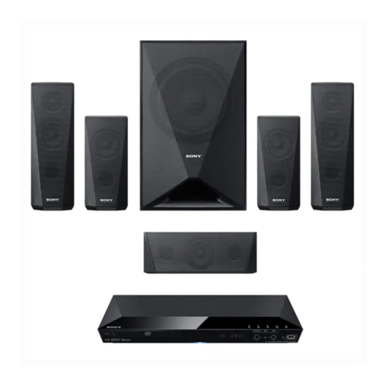
COMPONENT MODEL NAME
DAV-DZ350
DVD receiver
HBD-DZ350
Front speaker
SS-TS124
Center speaker
SS-CT123
Surround speaker
SS-TS123
Subwoofer
SS-WS123
• Please refer to service manual separatery issued for speakers and
subwoofer.
Amplifier Section
POWER OUTPUT (rated):
Front L + Front R
100 W + 100 W (at
3 ohms, 1 kHz, 1%
THD)
POWER OUTPUT (reference):
Front L/Front R/
Center/Surround L/
Surround R: 167 W
(per channel at
3 ohms, 1 kHz)
Subwoofer: 165 W (at
3 ohms, 100 Hz)
Inputs
AUDIO IN and OPTICAL IN jacks
CD/DVD System
Laser Diode Properties
Emission Duration:
Continuous
Laser Output*: Less
than 44.6 μW
* This output is the value measurement at a
distance of 200 mm from the objective lens
surface on the Optical Pick-up Block with
7 mm aperture.
USB Section
(USB) port:
Maximum current:
500 mA
Bluetooth section
Communication system
Bluetooth Specification
version 2.1 +
EDR (Enhanced Data
Rate)
Output
Bluetooth Specification
Power Class 2
Maximum communication range
Line of sight approx.
10 m*
1
Frequency band
2.4 GHz band
(2.4000 GHz -
2.4835 GHz)
Modulation method
FHSS (Freq Hopping
Spread Spectrum)
9-893-742-06
Sony Corporation
2014F33-1
©
2014.06
Published by Sony Techno Create Corporation
Photo: HBD-DZ650
DAV-DZ650
DAV-DZ950
HBD-DZ650
HBD-DZ950
SS-TS125
SS-TS125
SS-CT123
SS-CT123
SS-TS123
SS-TS125
SS-WS123
SS-WS123
SPECIFICATIONS
2
Compatible Bluetooth profiles*
A2DP (Advanced
Audio Distribution
Profile)
AVRCP 1.0 (Audio
Video Remote Control
Profile)
Supported Codecs*
3
SBC*
4
Transmission range (A2DP)
20 Hz - 20,000 Hz
(Sampling frequency
44.1 kHz)
1
*
The actual range will vary depending on
factors such as obstacles between devices,
magnetic fields around a microwave oven,
static electricity, cordless phone, reception
sensitivity, operating system, software
application, etc.
2
*
Bluetooth standard profiles indicate the
purpose of Bluetooth communication
between devices.
3
*
Codec: Audio signal compression and
conversion format
*
4
Subband Codec
Tuner Section
System
PLL quartz-locked
digital synthesizer
Tuning range
87.5 MHz -
108.0 MHz (50 kHz
step)
Antenna
FM lead antenna
Video Section
Outputs
VIDEO: Pin jack
HDMI OUT: HDMI
19-pin
General
Power requirements 220 V - 240 V AC,
50/60 Hz
Power consumption On: 70 W
Standby: 0.3 W*
* Valid when the system is in the following
status:
[Control for HDMI] is set to [Off ].
Dimensions (approx.) 430 mm × 54 mm ×
306 mm (w/h/d) incl.
projecting parts
Mass (approx.)
2.7 kg
Design and specifications are subject to
change without notice.
HBD-DZ350/DZ650/DZ950
South African Model
Model Name Using Similar Mechanism
DVD Mechanism Type
Optical Pick-up Block Name
Unpacking
DAV-DZ950
SS-TS125 (4)
Remote commander (remote) (1)
SS-CT123 (1)
Speaker packages
SS-WS123 (1)
DAV-DZ350
Sp
SS-TS124 (2)
For DAV-DZ950
SS-CT123 (1)
Base (4)
SS-TS123 (2)
Screw (16)
SS-WS123 (1)
FM wire antenna (aerial) (1)
DAV-DZ650
R6 (size AA) batteries (2)
SS-TS125 (2)
Video cord* (1)
SS-CT123 (1)
High Speed HDMI cable* (1)
SS-TS123 (2)
Operating Instructions
SS-WS123 (1)
* High Speed HDMI cable and video cord are
Speaker assembly parts for the tall speakers
included only in certain areas.
For DAV-DZ650
Base (2)
Screw (8)
DVD HOME THEATRE SYSTEM
AEP Model
DAV-DZ650/DZ950
Russian Model
DAV-DZ650
E Model
DAV-DZ350/DZ650/DZ950
Indian Model
DAV-DZ350
NEW
CMS-LS5FP
CMS-S79RFVP
eaker assembly parts for the tall speakers
DAV-DZ350/DZ650/DZ950
HBD-DZ350/DZ650/DZ950
DVD RECEIVER
Advertisement
Table of Contents

Related Manuals for Sony DAV-DZ350


Summary of Contents for Sony DAV-DZ350
- Page 1 Dimensions (approx.) 430 mm × 54 mm × Spread Spectrum) 306 mm (w/h/d) incl. projecting parts Mass (approx.) 2.7 kg Design and specifications are subject to change without notice. 9-893-742-06 Sony Corporation 2014F33-1 © 2014.06 Published by Sony Techno Create Corporation...
-
Page 2: Table Of Contents
The Bluetooth® word mark and logos are - POWER Board (Component Side) - ......32 registered trademarks owned by Bluetooth SIG, Inc. and any use of such marks by Sony 5-15. Printed Wiring Board Corporation is under license. Other - POWER Board (Conductor Side) - ......33 trademarks and trade names are those of their respective owners. - Page 3 DAV-DZ350/DZ650/DZ950 SECTION 1 SERVICING NOTES RELEASING THE DISC TRAY LOCK NOTES ON HANDLING THE OPTICAL PICK-UP The disc tray lock function for the antitheft of an demonstration BLOCK OR BASE UNIT disc in the store is equipped. The laser diode in the optical pick-up block may suffer electro-...
- Page 4 DAV-DZ350/DZ650/DZ950 Ver. 1.4 MODEL IDENTIFICATION CAPACITOR ELECTRICAL DISCHARGE PROCESSING – Rear view – When checking the board, the electrical discharge is necessary for the electric shock prevention. Connect the resistor to both ends of respective capacitors. • POWER board CE901 and CE902 –...
- Page 5 DAV-DZ350/DZ650/DZ950 HOW TO OPEN THE TRAY WHEN POWER SWITCH TURN OFF ditch – Bottom view – 1 Insert the tweezers etc. in the hole of the chassis, and slide the lever in the direction of the arrow. 2 Pull out the disc tray.
-
Page 6: Disassembly
DAV-DZ350/DZ650/DZ950 Ver. 1.3 SECTION 2 DISASSEMBLY • This set can be disassembled in the order shown below. 2-1. DISASSEMBLY FLOW 2-2. TOP COVER (DJ) (Page 6) 2-3. DVD DOOR ASSY 2-4. POWER BOARD (Page 7) (Page 7) 2-5. FRONT PANEL BLOCK (Page 8) 2-6. -
Page 7: Dvd Door Assy
DAV-DZ350/DZ650/DZ950 2-3. DVD DOOR ASSY 4 DVD door assy 3 five claws ditch – Bottom view – 1 Insert the tweezers etc. in the hole of the chassis, and slide the lever in the direction 2 Pull out the disc tray. -
Page 8: Front Panel Block
DAV-DZ350/DZ650/DZ950 2-5. FRONT PANEL BLOCK Wire setting DVD mechanism deck Bring the slack part to the front side. (CMS-LS5FP) wire tie POWER board 1 Cut two wire ties. claw claw Note 1: In reassembling, use new wire tie to fasten the clamp same as before. -
Page 9: Bt Antenna (Ant1), Power Key Board, Function Key Board
DAV-DZ350/DZ650/DZ950 2-6. BT ANTENNA (ANT1), POWER KEY BOARD, FUNCTION KEY BOARD Wire e i BT antenna (ANT1) POWER KEY board claw claw FUNCTION KEY board claw claw claw claw claw 6 two claws 1 four claws qa Remove the FUNCTION KEY board 7 POWER KEY board block in the direction of an arrow. -
Page 10: Dvd Mechanism Deck Block
DAV-DZ350/DZ650/DZ950 2-7. DVD MECHANISM DECK BLOCK 5 DVD mechanism deck block 3 two screws (BVTT3 3 two screws (BVTT3 4 Remove the DVD mechanism deck (CMS-LS5FP) in the 1 connector direction of the arrow. (CN101) 2 wire kit (FFC) (CN100) Note 1: When you install the connector, please install them correctly. -
Page 11: Dvd Mechanism Deck (Cms-Ls5Fp)
DAV-DZ350/DZ650/DZ950 2-8. DVD MECHANISM DECK (CMS-LS5FP) 5 DVD mechanism deck 3 two claws 1 connector (CMS-LS5FP) 2 connector – DVD mechanism deck bottom view – 4 wire kit (FFC) Note 1: When you install the connector, please ow to insta wi e kit install them correctly. -
Page 12: Holder Chuck
DAV-DZ350/DZ650/DZ950 Ver. 1.3 2-9. HOLDER CHUCK 5 holder chuck 2 Remove the holder chuck in the direction of the arrow. 1 claw 3 hook 1 claw 4 Remove the holder chuck in the direction of the arrow. 3 hook 2-10. TRAY DISC-1 •... -
Page 13: Tray Disc-2
DAV-DZ350/DZ650/DZ950 Ver. 1.3 2-11. TRAY DISC-2 2 Push the tray disc in the direction of the arrow with an index finger. tray disc 1 Pull the claw in the direction of the arrow with the thumb. 3 tray disc 2 Push the tray disc in the direction of the arrow with an index finger. -
Page 14: Optical Pick-Up Block-1
DAV-DZ350/DZ650/DZ950 Ver. 1.3 2-12. OPTICAL PICK-UP BLOCK-1 • Continued on next page. 1 Remove the solder. 1 Remove the solder. [blue] [red] Note: Don't remove these two solders. [black/red] Note: Don't remove these two solders. [green] 1 Remove the solder. -
Page 15: Optical Pick-Up Block-2
DAV-DZ350/DZ650/DZ950 Ver. 1.3 2-13. OPTICAL PICK-UP BLOCK-2 2 Rotate the gear [black] in the direction of the arrow B. – DVD mechanism deck top view – 1 Move the slide cam in the direction of the arrow A 3 Move the gear rack [white] in the direction of the arrow C. -
Page 16: Mic Board
DAV-DZ350/DZ650/DZ950 2-14. MIC BOARD Wire e i MIC board claw POWER board claw 1 connector (CN600) Note: When you install the connector, please install them correctly. There is a possibility that this machine damages when not correctly installing it. Insert is straight to the interior. -
Page 17: Main Board
DAV-DZ350/DZ650/DZ950 2-15. MAIN BOARD 3 heat sink screw 4 screw 4 two screws (BVTT3 (BVTT3 3 heat sink screw Note: When you install the connector, please 4 screw install them correctly. (BVTT3 There is a possibility that this machine damages when not correctly installing it. -
Page 18: Test Mode
DAV-DZ350/DZ650/DZ950 SECTION 3 TEST MODE VERSION DISPLAY Confi rmation procedure of version only: 1. Connect this unit with TV monitor. 2. Press the [ ] button to turn on the system. 3. Press the [ ] button. (State of “Tray open”) 4. -
Page 19: Troubleshooting
DAV-DZ350/DZ650/DZ950 Ver. 1.5 SECTION 4 TROUBLESHOOTING 3. Flow When “PROTECT” is Displayed 1. Mecha check fl ow Check that the “PROTECT” is Exchange the LOADER. tray opens and Check that the speakers are connected. Exchange the MAIN board. Part No. -
Page 20: Diagrams
DAV-DZ350/DZ650/DZ950 SECTION 5 DIAGRAMS 5-1. BLOCK DIAGRAM DVD/CD VFD ( 8 Grid x 14 Anode ) COMPONENT VIDEO OUT SDRAM FLASH EEPROM Same DL0 design SPK OUT 1000W VIDEO OUT 4M X 16 BTL OUTPUT IM CMS-S76RFS3G1 167W X 6 THD=30%... -
Page 21: Printed Wiring Board - Mic Board
DAV-DZ350/DZ650/DZ950 THIS NOTE IS COMMON FOR PRINTED WIRING BOARDS AND SCHEMATIC DIAGRAMS. 5-2. PRINTED WIRING BOARD - MIC Board - • : Uses unleaded solder. (In addition to this, the necessary note is printed in each block.) For Printed Wiring Boards. -
Page 22: Printed Wiring Board - Main Board (Component Side)
DAV-DZ350/DZ650/DZ950 5-4. PRINTED WIRING BOARD - MAIN Board (Component Side) - • See page 21 for Circuit Boards Location. • : Uses unleaded solder. MAIN BOARD (COMPONENT SIDE) Note: When the IC501, IC502 and IC503 on the MAIN board are re- placed, refer to “NOTE OF REPLACING THE IC501, IC502... -
Page 23: Printed Wiring Board - Main Board (Conductor Side)
DAV-DZ350/DZ650/DZ950 5-5. PRINTED WIRING BOARD - MAIN Board (Conductor Side) - • See page 21 for Circuit Boards Location. • : Uses unleaded solder. MAIN BOARD (CONDUCTOR SIDE) DAV-DZ350/DZ650/DZ950... -
Page 24: Schematic Diagram - Main Board (1/6)
DAV-DZ350/DZ650/DZ950 5-6. SCHEMATIC DIAGRAM - MAIN Board (1/6) - • See page 35 for IC Block Diagrams. MAIN BOARD (1/6) C150 C154 VCC5_RF FB100 VCC5 C151 C155 C100 100uF/10V FB101 C152 C156 VCC33_RF CN100 C102 CN24/0.5mm FPC 100uF/10V C153 C157... -
Page 25: Schematic Diagram - Main Board (2/6)
DAV-DZ350/DZ650/DZ950 5-7. SCHEMATIC DIAGRAM - MAIN Board (2/6) - • See page 41 for IC Pin Function Description. MAIN BOARD (2/6) MCLK MCLK VCC33 BCLK BCLK LRCK LRCK IC200 TSD0 TSD0 TSD1 TSD1 R203 TSD2 IIC_SCL TSD2 R204 IIC_SDA R205... -
Page 26: Schematic Diagram - Main Board (3/6)
DAV-DZ350/DZ650/DZ950 5-8. SCHEMATIC DIAGRAM - MAIN Board (3/6) - • See page 35 for IC Block Diagrams. MAIN BOARD (3/6) DQ0[0..15] A[1..21] IC100C IOA1 IOA2 IOA3 IOA4 MA[0..11] IOA5 IOA6 IOA7 IC300 HIGHA0 RA300 HIGHA1 RA301 HIGHA2 DQ10 IC301 HIGHA3... -
Page 27: Schematic Diagram - Main Board (4/6)
DAV-DZ350/DZ650/DZ950 5-9. SCHEMATIC DIAGRAM - MAIN Board (4/6) - MAIN BOARD (4/6) VCC33_RF IC100D FB400 L400 10uH VCC33 AVDD3 DACVDDA VCC33 L401 10uH VCC1V8 SVDD3 DACVDDB VCC33 PLLVDD3 VCC33 FB401 L402 10uH C401 ADCVDD3 C409 RFVDD3 APLLVDD C416 10uF/16V 100uF/16V... -
Page 28: Schematic Diagram - Main Board (5/6)
DAV-DZ350/DZ650/DZ950 5-10. SCHEMATIC DIAGRAM - MAIN Board (5/6) - • See page 35 for IC Block Diagrams. MAIN BOARD (5/6) R500 +12V 47UH P+12V R655 C751 4.7U/25V R639 1K 1% +3.3V D512 1N4148 SL&SR DET L500 +3.3V 2SD882 470K 1%... -
Page 29: Schematic Diagram - Main Board (6/6)
DAV-DZ350/DZ650/DZ950 5-11. SCHEMATIC DIAGRAM - MAIN Board (6/6) - • See page 35 for IC Block Diagrams. MAIN BOARD (6/6) R626 R628 C671 10uF/16V R618 CN600 R619 R620 R629 MIC-L C674 10uF/16V C651 150P C652 150P C653 MIC-R R622 VCC33... -
Page 30: Printed Wiring Boards - Panel Section
DAV-DZ350/DZ650/DZ950 5-12. PRINTED WIRING BOARDS - PANEL Section - • See page 21 for Circuit Boards Location. • : Uses unleaded solder. POWER KEY BOARD (COMPONENT SIDE) FUNCTION KEY BOARD (COMPONENT SIDE) FUNCTION KEY BOARD (CONDUCTOR SIDE) POWER KEY BOARD... -
Page 31: Schematic Diagram - Panel Section
DAV-DZ350/DZ650/DZ950 5-13. SCHEMATIC DIAGRAM - PANEL Section - • See page 35 for IC Block Diagrams. FUNCTION KEY BOARD VCC5# VFD-FUDABA(32PIN) -24V VFD800 L800 L801 47uH 47uH C800 ZD800 47uF/35V C801 C802 Q800 Transformer R800 C803 SC8050 47uF/10V 100uF/10V T800... -
Page 32: Printed Wiring Board - Power Board (Component Side)
DAV-DZ350/DZ650/DZ950 5-14. PRINTED WIRING BOARD - POWER Board (Component Side) - • See page 21 for Circuit Boards Location. • : Uses unleaded solder. POWER BOARD (COMPONENT SIDE) DAV-DZ350/DZ650/DZ950... -
Page 33: Printed Wiring Board - Power Board (Conductor Side)
DAV-DZ350/DZ650/DZ950 5-15. PRINTED WIRING BOARD - POWER Board (Conductor Side) - • See page 21 for Circuit Boards Location. • : Uses unleaded solder. POWER BOARD (CONDUCTOR SIDE) DAV-DZ350/DZ650/DZ950... -
Page 34: Schematic Diagram - Power Board
DAV-DZ350/DZ650/DZ950 5-16. SCHEMATIC DIAGRAM - POWER Board - • See page 35 for IC Block Diagrams. POWER BOARD CN902 ALL RES. ARE 1/6W EXCEPT SPECICAL EXPLAIN WITH NOTES TSB100006-0018 /0014 CN3P-396-R2 ALL EC.CAP. ARE 50V EXCEPT SPECICAL EXPLAIN WITH NOTES... - Page 35 DAV-DZ350/DZ650/DZ950 • IC Block Diagrams – MAIN Board – IC101 AM5888 MUTE MUTE BIAS VINFC 1 VINTK TRB1 2 REGO2 3 TRB2 VINSL+ 4 VINLD REGO1 5 VCTL VCC2 FWD 6 VCC2 DRIVER REV 7 VOLD– SPINDLE DRIVER (4x) VCC2...
- Page 36 DAV-DZ350/DZ650/DZ950 IC301 FLASH 32M BYTE# Q15/A–1 CONTROL WRITE INPUT PROGRAM/ERASE STATE LOGIC HIGH VOLTAGE MACHINE (WSM) FLASH X–DECODER ADDRESS RESET# ARRAY STATE ARRAY LATCH REGISTER SOURCE WP#/ACC BUFFER RY/BY Y–PASS Y–DECODER GATE COMMAND DATA DECODER SENSE DATA AMPLIFIER COMMAND DATA...
- Page 37 DAV-DZ350/DZ650/DZ950 IC500 TAS5538 PWM_HPM_L 1 PWM_HPP_L 2 PWM_HPM_R 3 PWM_HPP_R 4 AVSS 5 PLL_FLTM 6 PLL_FLTP 7 VR_ANA 8 AVDD 9 ASEL_EMO2 10 MCLK 11 OSC_RES 12 POWER DVSS2_CORE 13 SUPPLY DVDD2_CORE 14 PWM_P_6 PWM_M_6 EMO1 15 PWM_P_5 RESET 16...
- Page 38 DAV-DZ350/DZ650/DZ950 IC501 – 503 TAS5352A 44 GVDD_A 43 BST_A 42 NC GATE CONTROL TIMING RECEIVER DRIVE BTL/PBTL 41 PVDD_A CONFIGURATION 40 PVDD_A PULL DOWN RESISTOR OUT_A GND_A 37 GND_B BTL/PBTL CONFIGURATION PULL DOWN RESISTOR GATE CONTROL TIMING 36 OUT_B RECEIVER...
- Page 39 DAV-DZ350/DZ650/DZ950 IC601 CS8422 LEVEL TRANSLATORS RX0/RXP0 1 RX1/RXN0 2 RECEIVER CLOCK & DATA VA 3 RECOVERY (PLL) AGND 4 SAMPLE RATE RX2/RXP1 5 CONVERTER RX3/RXN1 6 SERIAL FORMAT AUDIO DETECT OUTPUT C OR U SERIAL DATA BUFFER AUDIO OSCLK2 (FIRST 5 BYTES)
- Page 40 DAV-DZ350/DZ650/DZ950 – POWER Board – IC903 SSC6200 +7.6 V +9.6 V CV/CC 20 A 410 A CONTROL FB/CC/OVP 1 VCC 2 +14.6 V/+10 V +8.5 V OVER LOAD OVER PROTECTION VOLTAGE +33.5 V +7.3 V PROTECT UNDER VOLTAGE 10 s...
- Page 41 DAV-DZ350/DZ650/DZ950 • IC Pin Function Description MAIN BOARD IC201 STM8S207 (Flash, EEPROM, ADC, Timers, UART, SPI, I²C) Pin No. Pin Name Description MCU reset OSCIN 16 MHz OSCOUT 16 MHz 4, 5 Vssio_1, VSS Ground VACP Capacitor connect to ground...
-
Page 42: Exploded Views
DAV-DZ350/DZ650/DZ950 Ver. 1.1 SECTION 6 EXPLODED VIEWS Note: • -XX and -X mean standardized parts, so • Abbreviation The components identifi ed by mark 0 they may have some difference from the : Turkish model or dotted line with mark 0 are critical for original one. -
Page 43: Front Panel Section
DAV-DZ350/DZ650/DZ950 6-2. FRONT PANEL SECTION supplied POWER KEY board ANT1 supplied supplied FUNCTION supplied KEY board not supplied Ref. No. Part No. Description Remark Ref. No. Part No. Description Remark 9-885-183-73 FRONT PANEL ASSY (DZ350) 3-087-053-01 +BVTP2.6 (3CR) 9-885-183-74 FRONT PANEL ASSY (DZ650) -
Page 44: Chassis Section
DAV-DZ350/DZ650/DZ950 Ver. 1.4 6-3. CHASSIS SECTION DVD mechanism deck section (CMS-LS5FP) FFC1 not supplied not supplied not supplied MAIN board not supplied supplied not supplied not supplied Note: Refer to the “CHANGES TO SPECIFICATIONS” on page 4 for how to distinguish new/former types of the MAIN board. (E3 and E93 models only) Ref. -
Page 45: Dvd Mechanism Deck Section (Cms-Ls5Fp)
DAV-DZ350/DZ650/DZ950 Ver. 1.5 6-4. DVD MECHANISM DECK SECTION (CMS-LS5FP) Ref. No. Part No. Description Remark Ref. No. Part No. Description Remark 9-885-194-42 LOADER 0 OP1 9-885-194-43 TRAVERSE (Optical pick-up block: CMS-S79RFVP) -
Page 46: Electrical Parts List
DAV-DZ350/DZ650/DZ950 Ver. 1.4 SECTION 7 FUNCTION KEY MAIN ELECTRICAL PARTS LIST POWER POWER KEY Note: • Due to standardization, replacements in • CAPACITORS : Russian model the parts list may be different from the uF: μF : South African model parts specifi... - Page 47 DAV-DZ350/DZ650/DZ950 Ver. 1.5 Ref. No. Part No. Description Remark Ref. No. Part No. Description Remark MISCELLANEOUS 1-492-337-11 REMOTE COMMANDER (RM-ADU162) (remote) ************** 9-885-166-93 FM ANTENNA (FM wire antenna (aerial)) 9-885-167-27 RCA CABLE (Video cord) (DZ350: EXCEPT E12/ 0 AC1 9-885-183-70...
- Page 48 Addition of Russian, Asian and Oceanian (Except Australian, Thai) models of DAV-DZ650 Addition of Asian and Oceanian (Except Australian, Thai) models of DAV-DZ350/DZ950 2013.10 Change of the VIDEO cable to the HDMI cable (DAV-DZ350: Indian model) (SMR-13037) 2014.03 Addition of DISASSEMBLY and EXPLODED VIEW of DVD mechanism deck (CMS-LS5FP) Addition of Part No.