
Related Manuals for Panasonic DMR-EH65EC


Summary of Contents for Panasonic DMR-EH65EC
- Page 1 ORDER NO.MAD0605017CE DVD Recorder DMR-EH65EC / DMR-EH65EP Vol.1 Colour (K).......Black Type (S).......Silver Type SPECIFICATIONS...
-
Page 2: Safety Precautions
2006 Matsushita Electric Industrial CO., Ltd. All rights reserved. Unauthorized copying and distribution is a violation of law. 1. SAFETY PRECAUTIONS 1.1. GENERAL GUIDELINES 1. Be careful during removing metal parts, sharp edges. 2. When servicing, observe the original lead dress. If a short circuit is found, replace all parts which have been overheated or damaged by the short circuit. - Page 3 the customer from being exposed to shock hazards. 1.1.1. LEAKAGE CURRENT COLD CHECK 1. Unplug the AC cord and connect a jumper between the two prongs on the plug. 2. Measure the resistance value, with an ohmmeter, between the jumpered AC plug and each exposed metallic cabinet part on the equipment such as screw heads, connectors, control shafts, etc.
-
Page 4: Prevention Of Electrostatic Discharge (Esd) To Electrostatic Sensitive (Es) Devices
and rechecked before it is returned to the customer. 2. WARNING 2.1. PREVENTION OF ELECTROSTATIC DISCHARGE (ESD) TO ELECTROSTATIC SENSITIVE (ES) DEVICES Some semiconductor (solid state) devices can be damaged easily by static electricity. Such components commonly are called Electrostatic Sensitive (ES) Devices. Examples of typical ES devices are integrated circuits and some field-effect transistor-sand semiconductor "chip"... -
Page 5: Precaution Of Laser Diode
8. Minimize bodily motions when handling unpackaged replacement ES devices. (Otherwise hamless motion such as the brushing together of your clothes fabric or the lifting of your foot from a carpeted floor can generate static electricity sufficient to damage an ES device). 2.2. -
Page 6: Service Caution Based On Legal Restrictions
2.3. SERVICE CAUTION BASED ON LEGAL RESTRICTIONS General description about Lead Free Solder (PbF) - The lead free solder has been used in the mounting process of all electrical components on the printed circuit boards used for this equipment in considering the globally environmental conservation. - The normal solder is the alloy of tin (Sn) and lead (Pb). -
Page 7: Service Navigation
control after setting the temperature at 350±30 degrees C (662±86°F). When soldering or unsoldering, please completely remove all of the solder on the pins or solder area and be sure to heat the soldering points with the Pb free solder until it melts enough. Definition of PCB Lead Free Solder being used - The letter of “Pbf is printed either foil side or component side using the lead free solder. -
Page 8: Caution For Divx
- Schematic Diagram, Block Diagram and P.C.B. layout of RAM/ Digital P.C.B. Module. - Parts List for individual parts of RAM/Digital P.C.B. Module. - Exploded View and Parts List for individual parts of RAM/Digital P.C.B. Module. 2. The following category are recycle module part. Please send them to Central Repair Center. - Page 9 Power supply: AC220-240 V, 50/60 Hz Power consumption: 34 W ±1,3 W Power save mode 2 W ± 0,4 W Dimensions and Mass: 430 (W) x 329 (D) x 58 (H) (excluding protrusions) / 4.2 kg Operating temperature +5 to +40 °C range: Operating humility range: 10 to 80 % RH (no condensation)
- Page 10 UHF: CH 21 - CH 68 RF Converter Output: not provided SD Card Slot: JPEG (Still Picture DCF Standard) TIFF (uncompressed) MPEG2 (rec. by Panasonic cam) Campatible Cards: SD Card, Multimedia Card miniSD Card (with adapter) Card format: FAT12, FAT16...
- Page 11 Video input AV1 / AV2: 21 pin connector (1.0 Vp- p 75 Video input AV3 / AV4: pin jack connector (1.0 Vp -p 75 S-Video input AV1 / AV2: 21 pin connector (Y: 1.0 Vp-p, C: 0.3 Vp-p S-Video input AV3 / AV4: pin jack connector (Y: 1.0 Vp-p, C: 0.3 Vp-p RGB Video input AV3...
-
Page 12: New Feature
5. NEW FEATURE 5.1. ABOUT DivX 5.1.1. GENERAL DivX is a new video compressing format that is applied MPEG-4 technology to improve quality and the compressibility and it is developed by the DivXNetworks, Inc., Video file of high resolution and the high picture quality can be made thought it is a high compressibility. - Page 13 - Number of remaining plays is reduced by one if - you press [POWER] - you press [STOP] - you press [backwards SKIP], / [backwards SLOW / SEARCH] or / [forwards SLOW / SEARCH] / etc. and arrive at another content or start of content being played.
- Page 14 Registration Code display (code is an example) Ovtainment/Playback of additional file after Activation (code/ID is an example) CASE 2 WHEN EEPROM OR P.C.B. INCLUDING EEPROM WAS REPLACED FOR REPAIRING CASE 3 WHEN RECORDER WAS EXCHANGED TO ANOTHER RECORDER FOR REPAIRING New Registration Code is displayed (code is an example) Case 2...
- Page 15 Activation: File obtaining (code/ID are example) Activation: File Playback Registration Code display after Activation (example) Obtainment/Playback od additional file after Activation (code/ID is an example) Case 3...
- Page 16 CASE 4 WHEN CUSTOMER OWN SECOND RECORDER Registration Code display of second recorder (code is an example) Case 4 Activation: File obtaining (code/ID are example) Activation: File Playback...
- Page 17 Registration Code display after Activation (example) Obtainment/Playback od additional file after Activation (code/ID is an example) CASE 5 WHEN OWNER OF RECORDER WAS CHANGED TO ANOTHER Case 5...
- Page 18 Activation Activation: File obtaining (code/ID are example) Activation: File Playback FILE KIND (There are two kinf of Activation files as follows too.) - Rental: There is a playback limitation - Purchase: Unrestricted Also there is next file as DRM files besides the above-mentioned. - Base: / It is not necessary to approve though the contents is being endode.
- Page 19 same as usual DivX file when seeing from user.) SCREEN SHIFT (Error display) Wheter approval is OK or not. Wheter the recorder is corresponding to User information on the file or not. 5.1.3. ABOUT DivX DRM Divx file includes file to which DRM(Digital Right Management) is applied and file not applied. This item is a content that relates only in treating file to which DRM is applied.
-
Page 20: Hdavi Control (Hdmi Link)
requests users to input yes or no. Following specifications have been installed for the rental files in the purpose to clarify the count condition of number of times of playback. - Conditions on counting number of times of play. 1. When a file was opened successfully. (At the time of playback start) 2. - Page 21 Cable Transmission Directionality Transmission Feature method signal Digital image Clock line in one system and data line in three systems can high-speed (none-compression One-way communicate high reliability because of high-definition balance communication that uses three television image) respectively every one system. Digital Audio Moreover, because high-speed data line (6ch/24 bit high sound...
- Page 22 VIErA. A. Starting of playback: It includes automatic playback of DVD-Video and so on. And it includes picture of screen saver too. B. GUI display: FUNCTIONS, DIRECT NAVIGATOR, TV PROGRAM, PROG/CHECK, Timer Recording, G-code, Initial setting, Playback setting, Play list, SD/DVD guide, Warning messages that user can select and so on.
-
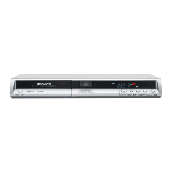
Page 23: Location Of Controls And Components
6. LOCATION OF CONTROLS AND COMPONENTS 7. OPERATING INSTRUCTIONS 7.1. TAKING OUT THE DISC FROM DVD-DRIVE UNIT WHEN THE DISC CANNOT BE EJECTED BY OPEN/CLOSE BUTTON 7.1.1. FORCIBLE DISC EJECT 7.1.1.1. WHEN THE POWER CAN BE TURNED OFF 1. Turn off the power and press [STOP], [CH UP] keys on the front panel simultaneously for 5 seconds. -
Page 24: Service Mode
5. Put deck upward and push out Tray by Eject Pin (JZS0484) or minus screw driver (small). 8. SERVICE MODE 8.1. SELF-DIAGNOSIS AND SPECIAL MODE SETTING 8.1.1. SELF-DIAGNOSIS FUNCTIONS Self-Diagnosis Function provides information for errors to service personnel by “Self-Diagnosis Display”... - Page 25 Error Diagnosis contents Description Monitor Automatic FL display Code Display IR ERR IR communication [IR ERR] is displayed when No display error communication between Timer microprocessor and IR microprocessor fails. No REC Recording is [No REC] is displayed when No display impossible recording is impossible due to the defect, dirt or wound of media.
- Page 26 Error Diagnosis contents Description Monitor Automatic FL display Code Display Inoperative fan motor When inoperative fan motor is No display No display detected after powered on, the power is turned off automatically. The event is saved in memory. No error information Initial setting for error code in No display No display...
- Page 27 Error Diagnosis contents Description Monitor Automatic FL display Code Display SELF Restoration operation Since the power cord fell out No display during a power CHECK failure or operation, it is under restoration operation. *It will OK, if a display disappears automatically.
-
Page 28: Test Mode
8.1.2. SPECIAL MODES SETTING Item FL display Key operation Mode name Description Front Key TEST Mode *All the main unit’s parameters Press [STOP], [CH UP] (include tuner) are initialized. and [OPEN/CLOSE] keys simultaneously for five seconds when power is off. Rating password The audiovisual level setting Open the tray, and press... - Page 29 Item FL display Key operation Mode name Description Front Key Forced power-off When the power button is not Display in P-off mode. Press [Power] key over effective while power is ON, turn than 10 seconds. off the power forcibly. *When Timer REC is ON or EXT- LINK is ON, execute “Forced Power-off”...
- Page 30 Item FL display Key operation Mode name Description Front Key Aging Contents (Example): Demonstration Ejection of the disc is prohibited. *When lock the tray. When the power is on, lock/unlock press [STOP] and The lock setting is effective until [POWER] keys unlocking the tray and not simultaneously for 5 released by “Main unit...
- Page 31 Item FL display Key operation Mode name Description Front Key ATP re-execution Re-execute ATP. Display at ATP executing. When the power is on ( mode), press [CH UP] and [CH DOWN] simultaneously for 5 seconds. Progressive The progressive setting is The display before When the power is on ( initialization...
- Page 32 Item FL display Key operation Mode name Description (Remote controller key) 1. Region code ROM Version Press [0] [2] in service (displayed for 5 sec.) Display mode 2. Main firm version (displayed for 5 sec.) 3. Timer firm version (displayed for 5 sec.) 4.
- Page 33 Item FL display Key operation Mode name Description (Remote controller key) RTSC Return in XP AV1 input signal is encoded (XP), Initial mode: EE2/ Interlace/ Press [1] [3] in service decoded (XP) and output XP/ Audio 48kHz mode. decoded signal to external (A &...
- Page 34 Item FL display Key operation Mode name Description (Remote controller key) HDD READ Perform a complete read When the HDD is OK Press [3] [1] in the service inspection inspection of the HDD. mode. * When canceling the checking mode while executing, do “forced If the HDD is defective power-off”.
- Page 35 Item FL display Key operation Mode name Description (Remote controller key) RAM Drive Last RAM Drive error code display. 1. Error Number is Press [4] [2] in service Error displayed for 5 seconds. mode. *For details about the drive error code, refer to the Service Manual When “INFO******”...
- Page 36 Item FL display Key operation Mode name Description (Remote controller key) 1. Insert DVD-RAM disc Laser power Drive state is judged based on into RAM Drive in service mode. confirmation difference between laser power (Other media are assumed to be value at shipping and present correspondence.) 2.
- Page 37 Item FL display Key operation Mode name Description (Remote controller key) Display the Error Display the Error History stored Display reason of error for Press [6] [5] in service History on the unit. mode. 5 seconds. Then press [0] [1] ~ [1] the past 19 error histories are displayed.
- Page 38 Item FL display Key operation Mode name Description (Remote controller key) SD card WRITE Check SD card WRITE function When the WRITE check is Insert a SC card to SD check with SD card slot. card slot, and press [7] in service mode.
-
Page 39: Service Fixture And Tools
Item FL display Key operation Mode name Description (Remote controller key) Error code Initialization of the last error code Press [9] [8] in service initialization held by timer (Write in F00) mode. Initialize Service Last Drive Error, Error history Press [9] [9] in service and Error Codes stored on the mode. - Page 40 10.2. P.C.B. POSITIONS 10.3. TOP CASE 1. Remove the 2 screws (A) and 3 screws (B). 2. Slide Top Case rearward and open the both ends at rear side of the Top Case a little and lift the Top Case in the direction of the arrows.
-
Page 41: Front Panel
10.4. FRONT PANEL 1. Unlock 2 tabs (A) and 3 tabs (B) in this order to remove Front Panel. The tab (A) and (B) should be unlocked at the same time, respectively. 10.5. SD CARD P.C.B. 1. Release FFC 2. Remove 2 Screws (A) to remove SD Card P.C.B. . -
Page 42: Ram/Digital P.c.b. Module
Caution: When replacing SD Card P.C.B., pay attention as below. 10.6. RAM/DIGITAL P.C.B. MODULE Caution: Pairing of RAM Drive and Digital P.C.B. as “RAM / Digital P.C.B. Module” have to be replaced together. If the pairing is changed, RAM Drive unit has to be re-aligned. - Page 43 Caution: When replacing Digital P.C.B., pay attention as below. 1. Remove 3 Screws on DVD-RAM Drive. 2. Remove 2 FFCs and 4 Screws. 3. Lift up Digital P.C.B. slightly to disconnect Main P.C.B. Connector and DV IN P.C.B. Connector on the bottom side.
- Page 44 4. Put Digital P.C.B. on DVD-RAM Drive and remove RAM/Digital P.C.B. Module. Note: RAM/Digital P.C.B. Module as service part has no heat sink unit. Before returning to customer, heat sink unit should be installed on to Digital P.C.B.
- Page 45 10.7. DV IN P.C.B. 1. Remove 1 Screw to remove DV IN P.C.B.
-
Page 46: Hard Disc Drive
10.8. HARD DISC DRIVE Caution: Writing the main firmware to the unit is necessary after replacing the HDD. Prepare the latest firmware updating disc. * The main firmware is recorded in the HDD, but the replacement HDD has no data (and needs to be formatted). Writing Procedure of Main Firm: - Writing of Main Firm needs 3, 4 minutes. - Page 47 11. [HELLO] [SELF CHECK] are displayed on FL 12. [UNFORMATED] is displayed on FL 13. After [UNFORMAT] was displayed, message to request FORMAT is displayed on TV screen 14. Select [Yes] and press [ENTER] key to format HDD (After FORMAT, program in HDD will be lost, but Main firm will not be lost “Write of the main farm”...
- Page 48 Handling of HDD The following precautions should be taken when handling HDD. 1. Never give an impact to HDD. (Even a drop from 1 cm height can be a cause of HDD failure). 2. When placing HDD on a workbench, provide a mat on a bench for shock absorption and anti-static purposes.
-
Page 49: Rear Panel
2. Remove 3 Screws and disconnect the 2 Connectors. 3. Lift up Power P.C.B. a little upwards and remove the P.C.B. sideways out of the Guide Pins. Note: When inserting P.C.B. confirm correct positions of Guide Pins. 10.10. REAR PANEL 1. - Page 50 2. Remove 7 Screws (A) and 2 Screws (B). 3. Unlock 2 Locking Tabs to remove Rear Panel. 10.10.1. FAN MOTOR 1. Disconnect Fan Connector. 2. Remove the 2 Screws. 3. Push and unlock 2 locking Tabs to remove Fan Motor.
- Page 51 10.11. MAIN P.C.B. AND FRONT P.C.B. 1. Remove 2 Screws from Main P.C.B. . 2. Remove 1 Screw from Front P.C.B. . 3. Pull out Main P.C.B. together with Front P.C.B. . Note: When inserting P.C.B. confirm correct positions of Guide Pins.
-
Page 52: Tuner P.c.b. / And Tuner
10.12. TUNER P.C.B. / AND TUNER 1. Pull out the Tuner P.C.B. in the direction of the arrow. 2. Remove Solder and pull out Tuner from Tuner P.C.B. . - Page 53 10.13. HDMI P.C.B. 1. Disconnect FFC Connector. 2. Pull out the HDMI P.C.B. in the direction of the arrow.
-
Page 54: Measurements And Adjustments
Caution: When replacing HDMI P.C.B., pay attention as below. 11. MEASUREMENTS AND ADJUSTMENTS... -
Page 55: Service Positions
11.1. SERVICE POSITIONS Note: For description of the disassembling procedure, see the section ASSEMBLING AND DISASSEMBLING (DISASSEMBLY FLOW CHART). 11.1.1. CHECKING AND REPAIRING OF POWER P.C.B. 1. Top Case - Remove 2 Screws (A) on side - Remove 3 rear Screws (B) on rear - Remove Top Case 2. - Page 56 11.1.2. CHECKING AND REPAIRING OF MAIN P.C.B. 1. Top Case - Remove 2 Screws (A) on side and 3 rear Screws (B) - Remove Top Case 2. Front Panel - Unlock 2 Locking Tabs on the side and 3 Locking Tabs on bottom - Remove Front Panel 3.
- Page 57 - Remove 2 Screws fixing Digital P.C.B. Angle 7. Main P.C.B. - Remove 2 Screws from Main P.C.B. - Remove Screw from Front P.C.B. - Unlock Main P.C.B. and Front P.C.B. from Bottom Plate - Hold Hard Disc Drive and Digital P.C.B. carefully and put it together with Main P.C.B.
- Page 58 - Lift up SD Card P.C.B. and wrap it with insulation sheet. 4. HDD - Remove 4 Screws fixing HDD Angle to remove it with HDD - Disconnect FFC from HDD 5. RAM/Digital P.C.B. Module - Remove 4 Screws fixing DVD-RAM Drive - Disconnect FFC from HDMI P.C.B.
- Page 59 - Remove 2 Screws (A) on side - Remove 3 rear Screws (B) on rear - Remove Top Case 2. Hard Disc Drive - Remove 4 Screws of HDD Angle from Main P.C.B. - Remove HDD ATAPI Connector - Remove Power Cable from HDD - Remove 2 Screws from HDD to disconnect HDD Angle - Put Replacement HDD on Insulation Board - Connect Extension Cable:...
-
Page 60: Caution For Replacing Parts
11.2. CAUTION FOR REPLACING PARTS 11.2.1. ITEMS THAT SHOULD BE DONE AFTER REPLACING PARTS * Note 1: (Resetting Method) Resetting object Condition of power Short Terminal IC7501 (Timer IC) POWER ON IC7502-4 (Reset_L) and (GND) * Note 2: Please will always pass the customer “Warning for Customers Who Use the DivX Video-on-Demand content.”... - Page 61 you unavoidably exchange EEPROM or P.C.B. including EEPROM (When the product is exchanged, it is the same.). You must use print attached to service part (EEPROM or P.C.B. including EEPROM) or must use copy of print below as “Warning for Customers who use the DivX Video-on-Demand content.”Information needed without fail for the customer for whom it is used continuing DivX Video-on-Demand Service to “Manual for the customer”...
-
Page 62: Standard Inspection Specifications After Making Repairs
5. Tray opens automatically 6. Insert updating disc for Firmware and press OPEN / CLOSE key (If a wrong disc was insered, [NG DISK] [NO FVU] is displayed on FL.) 7. [LOAD] [LD FVU] [M_FIRM] are displayed on FL alternately 8. - Page 63 Turn on the power, and confirm items pointed out. Items pointed out should reappear. Insert RAM disc. The Panasonic RAM disc should be recognized. Enter the EE (TU IN / AV IN - AV OUT) mode. No abnormality should be seen in the picture, sound or operation.
- Page 64 INITIAL/LOGO ABBREVIATIONS DACCK D/A CONVERTER CLOCK DEEMP DEEMPHASIS BIT ON/OFF INITIAL/LOGO ABBREVIATIONS DEMPH DEEMPHASIS SWITCHING A0~UP ADDRESS DIG0~UP FL DIGIT OUTPUT ACLK AUDIO CLOCK DATA INPUT AD0~UP ADDRESS BUS DMSRCK DM SERIAL DATA READ CLOCK ADATA AUDIO PES PACKET DATA DMUTE ADDRESS LATCH ENABLE DIGITAL MUTE CONTROL...
- Page 65 INITIAL/LOGO ABBREVIATIONS LDON LASER DIODE CONTROL LASER POWER CONTROL LRCK L CH/R CH DISTINCTION CLOCK INITIAL/LOGO ABBREVIATIONS MA0~UP MEMORY ADDRESS SBI0, 1 SERIAL DATA INPUT MEMORY CLOCK SBO0 SERIAL DATA OUTPUT MCKI MEMORY CLOCK INPUT SBT0, 1 SERIAL CLOCK MCLK MEMORY SERIAL COMMAND CLOCK SERIAL DATA CLOCK...
-
Page 66: Block Diagram
INITIAL/LOGO ABBREVIATIONS TRACKING ERROR TIBAL BALANCE CONTROL BALANCE OUTPUT 1 BALANCE INPUT BALANCE INPUT BALANCE OUTPUT 2 INITIAL/LOGO ABBREVIATIONS TPSN OP AMP INPUT TPSO OP AMP OUTPUT X' TAL TPSP OP AMP INVERTED INPUT XALE X ADDRESS LATCH ENABLE TRCRS TRACK CROSS SIGNAL XAREQ X AUDIO DATA REQUEST... -
Page 67: Printed Circuit Board
13.4. MAIN AV IO 13.5. MAIN TIMER 13.6. MAIN NICAM 13.7. TUNER 13.8. SD CARD / FRONT / DV IN 13.9. HDMI 14. PRINTED CIRCUIT BOARD 14.1. POWER P.C.B. 14.2. MAIN P.C.B. 14.3. TUNER P.C.B. / DV IN P.C.B. 14.4. SD CARD P.C.B. / FRONT P.C.B. 14.5. -
Page 68: Packing & Accessories Section
16.2. PACKING & ACCESSORIES SECTION... -
Page 69: Replacement Parts List
17. REPLACEMENT PARTS LIST Notes: *Important safety notice: Components identified by mark have special characteristics important for safety. Furthermore, special parts which have purposes of fire-retardant (resistors), high-quality sound (capacitors), low-noise (resistors), etc. are used. When replacing any of components, be sure to use only manufactures specified parts shown in the parts list. -
Page 70: Casing Parts & Printed Circuit Boards
*Parts mentioned [SPC] are supplied from PAVC *The 1, 2, 3 in the Remarks column shows the models as follows: 1 = DMR-EH65EP-S 2 = DMR-EH65EC-K 3 = DMR-EH65EC-S No indication = all models 17.1. CASING PARTS & PRINTED CIRCUIT BOARDS... - Page 71 Remarks Ref. No. Part No. Part Name & Description VEP70161A FRONT PCB 1,2,3 (RTL) VEP73135A DV IN PCB 1,2,3 (RTL) RFKB79119LT MAIN PCB 2,3 (RTL) RFKB79119MT MAIN PCB 1 (RTL) RMX0364 SPACER 1,2,3 RGR0365C-C REAR PANEL RGR0365C-M REAR PANEL RHD30111-3 SCREW 1,2,3 RHD30119-L...
-
Page 72: Packing & Accessories Parts
Remarks Ref. No. Part No. Part Name & Description RHD30113 SCREW TOP CASE SIDE RHD30113-1K SCREW TOP CASE SIDE RFKV0071HDK HDD ASSEMBLY 1,2,3 RKM0552A-S TOP PANEL RKM0552A-K TOP PANEL RMN0857 HDD BRACKET 1,2,3 RMC0625 TUNER GND 1,2,3 VEK0J99 MAIN-HDD CABLE 1,2,3 VMC1534 EARTH SPRING... -
Page 73: Electrical Parts
Remarks Ref. No. Part No. Part Name & Description EUR7659Y60 REMOTE CONTROL EUR7659YC0 REMOTE CONTROL UR76EC5903 BATTERY COVER 1,2,3 RJA0043-1C POWERCORD 1,2,3 K1TWACC00001 RF CABLE 1,2,3 K2KA6BA00003 AV CORD 1,2,3 RPQFD0001 ACCESSORY BOX 1,2,3 RPFD0005 PE-BAG RPFD0007 PE-BAG RPQD0003 1,2,3 RQT8432-L O/I BOOK (Eng Cont.) RQT8433-D... - Page 74 Remarks Ref. No. Part No. Part Name & Description C1511 ECJ1VB1A105K CHIP CAPACITOR 1,2,3 C1512 ECJ1VB1A105K CHIP CAPACITOR 1,2,3 C1515 F2A1E4700048 ALU ELEC CAPACITOR 1,2,3 C1516 F2A1H1510006 ALU ELEC CAPACITOR 1,2,3 C1518 F2A0J6810007 ALU ELEC CAPACITOR 1,2,3 C1519 ECJ1VB1A105K CHIP CAPACITOR 1,2,3 C1520 ECJ1VB1A105K...
- Page 75 C3017 F1H1C104A042 CHIP CAPACITOR 1,2,3...
- Page 76 Remarks Ref. No. Part No. Part Name & Description C3018 F1H1C104A042 CHIP CAPACITOR 1,2,3 C3019 F1H1C104A042 CHIP CAPACITOR 1,2,3 C3020 F1H1C104A042 CHIP CAPACITOR 1,2,3 C3021 F1H1C104A042 CHIP CAPACITOR 1,2,3 C3022 F1H1C104A042 CHIP CAPACITOR 1,2,3 C3024 F1H0J1050012 CHIP CAPACITOR 1,2,3 C3025 F1H1C104A042 CHIP CAPACITOR 1,2,3...
- Page 77 C4028 F2A1V100A534 ALU ELEC CAPACITOR 1,2,3...
- Page 78 Remarks Ref. No. Part No. Part Name & Description C4033 F2A1C220B173 ALU ELEC CAPACITOR 1,2,3 C4034 F2A1C220B173 ALU ELEC CAPACITOR 1,2,3 C4055 F1H1C104A008 CHIP CAPACITOR 1,2,3 C4056 F2A1C471A628 ALU ELEC CAPACITOR 1,2,3 C4057 ECJ2VC1H330J CHIP CAPACITOR 1,2,3 C4059 ECQV1H104JL3 PLAST FILM CAPACITOR 1,2,3 C4060 ECJ2VC1H330J...
- Page 79 C56133 ECJ1VB1A105K CHIP CAPACITOR 1,2,3...
- Page 80 Remarks Ref. No. Part No. Part Name & Description C56134 ECJ1VB1A105K CHIP CAPACITOR 1,2,3 C56135 ECJ0EB1A104K CHIP CAPACITOR 1,2,3 C56140 ECJ0EB1A104K CHIP CAPACITOR 1,2,3 C6801 F1H1H1030006 CHIP CAPACITOR 1,2,3 C6802 F1H1A225A051 CHIP CAPACITOR 1,2,3 C7301 F1H1C104A042 CHIP CAPACITOR 1,2,3 C7303 ECA1CAK101XB ALU ELEC CAPACITOR 1,2,3...
- Page 81 C7517 ECJ1VC1H180J CHIP CAPACITOR 1,2,3...
- Page 82 Remarks Ref. No. Part No. Part Name & Description C7518 ECJ1VC1H220J CHIP CAPACITOR 1,2,3 C7519 ECJ1VC1H180J CHIP CAPACITOR 1,2,3 C7520 F1H1C104A042 CHIP CAPACITOR 1,2,3 C7522 F1H1H1010005 CHIP CAPACITOR 1,2,3 C7523 F1H1H1030006 CHIP CAPACITOR 1,2,3 C7524 F1H1C104A042 CHIP CAPACITOR 1,2,3 C7528 F1H1C104A042 CHIP CAPACITOR 1,2,3...
- Page 83 D1156 MA2C165001VT DIODE 1,2,3 Remarks Ref. No. Part No. Part Name & Description D1157 B0HADV000001 DIODE 1,2,3 D1270 B0JBSG000010 DIODE 1,2,3 ZA1270 VSC5614 HEAT SINK 1,2,3 D1601 B0JCPD000021 DIODE 1,2,3 D1701 B0JCPD000021 DIODE 1,2,3 D1800 MA2J11100L CHIP DIODE 1,2,3 D3901 MA2C165001VT DIODE 1,2,3...
- Page 84 Remarks Ref. No. Part No. Part Name & Description IC7302 C0EAH0000051 RESET IC 1,2,3 IC7401 C0CBCYG00004 POWER SUPPLY IC 1,2,3 IC7402 C0CBCDC00052 POWER SUPPLY IC 1,2,3 IC7403 C0CBCDD00025 POWER SUPPLY IC 1,2,3 IC7404 RFKFM6016KT EEPROM IC 1,2,3 [SPC] IC7501 C2CBJG000728 INTEGRATED CIRCUIT 1,2,3 IC7502 C0EBE0000504...
- Page 85 Remarks Ref. No. Part No. Part Name & Description LB3005 J0JBC0000011 BEAD CORE 1,2,3 LB3006 J0JBC0000019 COIL (RLBV252AV-Y) 1,2,3 LB3007 J0JBC0000011 BEAD CORE 1,2,3 LB3008 J0JBC0000019 COIL (RLBV252AV-Y) 1,2,3 LB3009 D0YBR0000020 CHIP RESISTOR 1,2,3 LB3010 D0YBR0000020 CHIP RESISTOR 1,2,3 LB3011 D0YBR0000020 CHIP RESISTOR 1,2,3 LB3012 J0JBC0000011...
- Page 86 LB7507 D0YBR0000020 CHIP RESISTOR 1,2,3...
- Page 87 Remarks Ref. No. Part No. Part Name & Description LB7508 D0YBR0000020 CHIP RESISTOR 1,2,3 LB7509 J0JCC0000060 BEAD CORE 1,2,3 LB7510 D0YBR0000020 CHIP RESISTOR 1,2,3 LB7515 D0YBR0000020 CHIP RESISTOR 1,2,3 LB7516 D0YBR0000020 CHIP RESISTOR 1,2,3 LB7517 D0YBR0000020 CHIP RESISTOR 1,2,3 LB7802 J0JHC0000032 BEAD CORE 1,2,3 LB7803 J0JHC0000032...
- Page 88 Remarks Ref. No. Part No. Part Name & Description QR1800 B1GDCFNN0002 TRANSISTOR 1,2,3 QR1801 B1GBCFNN0004 TRANSISTOR 1,2,3 QR4002 B1GDCFJJ0008 DIGITAL TRANSISTOR 1,2,3 QR4003 B1GBCFJJ0007 TRANSISTOR 1,2,3 QR4004 B1GBCFJJ0007 TRANSISTOR 1,2,3 QR7401 B1GBCFNN0009 TRANSISTOR 1,2,3 QR7402 B1GDCFLL0012 TRANSISTOR 1,2,3 QR7403 B1GBCFJA0006 TRANSISTOR 1,2,3 QR7404 B1GBCFJA0006...
- Page 89 R3008 D0GB102JA057 CHIP RESISTOR 1,2,3...
- Page 90 Remarks Ref. No. Part No. Part Name & Description R3009 D0GB104JA057 CHIP RESISTOR 1,2,3 R3054 D0GB750JA057 CHIP RESISTOR 1,2,3 R3055 D0GB750JA057 CHIP RESISTOR 1,2,3 R3056 D0GB750JA057 CHIP RESISTOR 1,2,3 R3057 D0GB750JA057 CHIP RESISTOR 1,2,3 R3058 D0GB750JA057 CHIP RESISTOR 1,2,3 R3059 D0GB750JA057 CHIP RESISTOR 1,2,3...
- Page 91 R4057 D0HB123ZA002 METAL FILM RESISTOR 1,2,3...
- Page 92 Remarks Ref. No. Part No. Part Name & Description R4066 D0HB103ZA002 METAL FILM RESISTOR 1,2,3 R4067 D0HB103ZA002 METAL FILM RESISTOR 1,2,3 R4071 D0GB473JA057 CHIP RESISTOR 1,2,3 R4074 D0GB473JA057 CHIP RESISTOR 1,2,3 R4076 D0GB821JA057 CHIP RESISTOR 1,2,3 R4077 D0GB101JA057 CHIP RESISTOR 1,2,3 R4078 D0GB272JA057...
- Page 93 R56140 ERJ2GEJ8R2X RESISTOR 1,2,3...
- Page 94 Remarks Ref. No. Part No. Part Name & Description R56142 ERJ2GEJ330X RESISTOR 1,2,3 R56143 ERJ2GEJ330X RESISTOR 1,2,3 R56144 ERJ2GEJ8R2X RESISTOR 1,2,3 R56145 ERJ2GEJ8R2X RESISTOR 1,2,3 R56146 ERJ2GEJ8R2X RESISTOR 1,2,3 R56147 ERJ2GEJ8R2X RESISTOR 1,2,3 R56148 ERJ2GEJ8R2X RESISTOR 1,2,3 R56149 ERJ2GEJ8R2X RESISTOR 1,2,3 R56150 ERJ2GEJ8R2X RESISTOR...
- Page 95 R7501 D0GB102JA057 CHIP RESISTOR 1,2,3...
- Page 96 Remarks Ref. No. Part No. Part Name & Description R7502 D0GB392JA057 CHIP RESISTOR 1,2,3 R7503 D0GB104JA057 CHIP RESISTOR 1,2,3 R7504 D0GB102JA057 CHIP RESISTOR 1,2,3 R7505 D1BB1502A010 CHIP RESISTOR 1,2,3 R7506 D0GB104JA057 CHIP RESISTOR 1,2,3 R7507 D1BB15010002 CHIP RESISTOR 1,2,3 R7508 ERJ3GEYF562V CHIP RESISTOR 1,2,3...
- Page 97 R7579 D0GB223JA057 CHIP RESISTOR 1,2,3...
- Page 98 Remarks Ref. No. Part No. Part Name & Description R7582 D0GB104JA057 CHIP RESISTOR 1,2,3 R7583 D0GB472JA057 CHIP RESISTOR 1,2,3 R7584 D0GB473JA057 CHIP RESISTOR 1,2,3 R7585 D0GB225JA057 CHIP RESISTOR 1,2,3 R7586 D0GB273JA057 CHIP RESISTOR 1,2,3 R7587 D0GB224JA057 CHIP RESISTOR 1,2,3 R7588 D0GB104JA057 CHIP RESISTOR 1,2,3...
- Page 99 S7504 EVQ11A04M TOUCH SWITCH 1,2,3 Remarks Ref. No. Part No. Part Name & Description S7505 EVQ11A04M TOUCH SWITCH 1,2,3 S7506 EVQ11A04M TOUCH SWITCH 1,2,3 S7507 EVQ11A04M TOUCH SWITCH 1,2,3 S7508 EVQ11A04M TOUCH SWITCH 1,2,3 T1150 ETS28BF1W6AD TRANSFORMER 1,2,3 T7501 G4D1A0000117 SWITCH.
- Page 100 Remarks Ref. No. Part No. Part Name & Description W524 D0YBR0000020 CHIP RESISTOR 1,2,3 W525 D0YBR0000020 CHIP RESISTOR 1,2,3 W526 D0YBR0000020 CHIP RESISTOR 1,2,3 W527 D0YBR0000020 CHIP RESISTOR 1,2,3 W528 D0YBR0000020 CHIP RESISTOR 1,2,3 W529 D0YBR0000020 CHIP RESISTOR 1,2,3 W529 ERJ6GEY0R00Z CHIP RESISTOR 1,2,3...
- Page 101 Remarks Ref. No. Part No. Part Name & Description RFKZ0260 Extension Cable Same as EH50 Main PCB - RAM/Digital PCB series 88 Pin (SPC) RFKZ0216 Extension Cable Same as EH55/ Main PCB - Power PCB EH56 series 23 Pin (SPC) RFKZ0366 Extension FFC Same as E55/E65 series...
- Page 102 T1150-12 STOP T1150-4,5 STOP IC1150-1 STOP T1150-8 STOP 10Vp-p (2m sec.div) 30Vp-p (5 sec.div) 10.0Vp-p (5 sec.div) 30Vp-p (5 sec.div) IC1150-9 STOP P7402-29,31 REC/PLAY P7402-51 REC/PLAY P7402-55 REC/PLAY 580Vp-p (5 sec.div) 0.8Vp-p (1m sec.div) 1.0Vp-p (20 sec.div) 0.8Vp-p (20 sec.div) P7402-67 REC/PLAY P7402-71 REC/PLAY P7402-63 REC/PLAY...
- Page 103 Q7802 Ref No. MODE PLAY STOP...
- Page 104 IC1150 IC1200 Ref No. MODE 11.6 -1523 PLAY 11.6 -1523 STOP 11.6 -1538 IC1601 IC1701 Ref No. MODE 12.3 12.3 12.4 12.4 PLAY 12.3 12.3 12.4 12.4 STOP 12.3 12.3 12.4 12.4 Q1200 Q1600 Ref No. MODE 12.3 12.3 12.3 PLAY 12.3 12.3...
- Page 105 P59001 Ref No. MODE 12.3 12.3 PLAY 12.3 12.3 STOP 12.3 12.3 P59001 Ref No. MODE PLAY STOP P59001 Ref No. MODE PLAY STOP P59001 Ref No. MODE 12.3 12.3 12.3 12.3 12.3 12.3 PLAY 12.3 12.3 12.3 12.3 12.3 12.3 STOP 12.3...
- Page 106 Switch button of the AV input between AV1, AV2 INPUT AUDIO STATUS DISPLAY TIME SLIP ShowView menu SELECT AV3 (front), AV4 and DV in. Panasonic SLOW/SEARCH DELETE Search or slow motion playback. Delete items DVD/TV Stops recording, replay or forward / reverse action STOP Starts playback.
- Page 107 Q1501 Q1509 Ref No. MODE 12.4 12.4 12.4 12.3 12.3 12.3 12.3 PLAY 12.4 12.4 12.4 12.3 12.3 12.3 12.3 STOP 12.4 12.4 12.4 12.3 12.3 12.3 12.3 Q4006 Q4007 Q4008 Q4009 Q7401 Ref No. MODE -0.1 -0.1 -0.1 -0.1 11.6 PLAY -0.1...
- Page 108 IC4009 IC4011 Ref No. MODE 11.6 PLAY 11.6 STOP 11.6 IC4012 IC4901 Ref No. MODE 11.6 PLAY 11.6 STOP 11.6 IC7301 Ref No. MODE PLAY STOP IC7301 Ref No. MODE PLAY STOP IC7301 Ref No. MODE PLAY STOP IC7302 IC7401 IC7402 Ref No.
- Page 109 IC1505 IC1506 Ref No. MODE PLAY STOP IC1507 IC1510 IC1520 Ref No. MODE PLAY STOP IC1521 IC1522 Ref No. MODE PLAY STOP Ref No. IC3001 MODE PLAY STOP IC3001 Ref No. MODE PLAY STOP IC3001 Ref No. MODE 11.6 PLAY 11.6 STOP 11.6...
- Page 110 AUDIO_OUT SIF_OUT UNREG_38V C7813 TUNER_VIDEO1 (TO MAIN) RFAGC C7825 R7818 SW(VIF) R7815 C7818 R7816 C7819 R7846 TL7401 AFT OUT AUDIO OUT C7838 R7845 SIF OUT R7811 BTL+30VIN 5V(VIF) VIDEO OUT LB7804 K7809 R7820 Q7802 R7844 DMR-EH65EC DMR-EH65EP TUNER SCHEMATIC DIAGRAM...
- Page 111 IC-DET AIL BLOCK DIAGRAM IC-DET AIL BLOCK DIAGRAM IC-DET AIL BLOCK DIAGRAM R7641 B-IN 1 2 3 4 5 6 4 3 2 BOUT B+IN R7643 VOUT R7644 S7508 R7640 DMR-EH65EC R7639 R7642 DMR-EH65EP Vref Vref MAIN TIMER AOUT A-IN A+IN SCHEMATIC DIAGRAM...
- Page 112 DET./ONDEAD TIMER CNT. CONTROL SOFT-DRIVE CIRCUIT CIRCUIT COMP STANDBY CIRCUIT OCP THRESHOLD COMPARATOR/ RESTERT DMR-EH65EC BURST MODE Important Safety Notice: TIMER UVLOcomp OCP THRESHOLD COMPARATOR Components identified with the mark have DMR-EH65EP ON WIDTH the special characteristics for safety. Note:...
- Page 113 POWER SCK/AF21 OUT L SUPPLY AMPLIFIER AMPLIFIER FM DEMODULATOR FM DEMODULATOR NARROW-BAND NARROW-BAND PLL SC2 PLL SC1 C7317 G_IIC_CLK_A C7313 C7312 G_IIC_DATA_A G_DEC_R_A G_DEC_L_A R7319 R7315 C7318 R7314 (EC) (EC) C7310 C7309 R7317 (EC) DMR-EH65EC DMR-EH65EP MAIN NICAM SCHEMATIC DIAGRAM...
- Page 114 UARTP2M LB7412 UARTM2P P_OFF_L3 R7409 CSYNC_IN LB7409 ANA3R3V LB7420 EPG_ON_H/BUSY LB7405 X_SW3R8V X_SW3R8V LB7402 X_SW_12V X_SW_12V X_SW_12V X_SW_12V X_SW_12V X_SW_12V LB7403 ANA5V DGND EPG_VIDEO DGND LOCATION MAP RGB_CPSVIN DGND R_IN 6-10 ZJ7405 DMR-EH65EC DMR-EH65EP MAIN NET SECTION 4/4 SCHEMATIC DIAGRAM...
- Page 115 CPNCIN_DM DGND C1548 BS_ON C1521 DGND G_IN DGND B_IN IC1506 DR +5V SWITCHING REGULA TOR IC-DET AIL BLOCK DIAGRAM VOUT ZJ7406 LOCATION MAP SENSE ON: H ON/OFF REG. DRIVE 6-10 PROTECTION VREF DMR-EH65EC DMR-EH65EP MAIN NET SECTION 3/4 SCHEMATIC DIAGRAM...
- Page 116 IC-DET AIL BLOCK DIAGRAM IICCLK IICDATA AUDIOOUT SIFOUT UNREG38V TUNERVIDEOIN VOUT SENSE (TUNER PACK) G_SIFIN_A G_TU_A_IN_A ZJ7403 BOOSTER 5V LOCATION MAP IC7401 GND CNT K7403 6-10 C7439 C7401 Q7402 R7446 UNREG_38V DMR-EH65EC DMR-EH65EP MAIN NET SECTION MAIN NET SECTION 2/4 (4/4) SCHEMATIC DIAGRAM...
- Page 117 LB1502 X_SW12V X_SW12V C1518 C1515 X_SW12V X_SW12V LB1506 X_SW3R8V X_SW3R8V P_ON_H X_SW3R8V DMR-EH65EC P_SAVE_L FANLOCK DMR-EH65EP FAN_GND MAIN NET SECTION MAIN NET SECTION 1/4 FANOUT (3/4) IMPORTANT SAFETY NOTICE: COMPONENTS IDENTIFIED WITH THE MARK HAVE THE SPECIAL CHARACTERISTICS FOR SAFETY.
- Page 118 BIAS CIRCUIT (SA1L) AV2 R/C AV2 R/C AV2 V/Y CLAMP BUFF. TUNER V SLICER TUN Rch AV1 Lch MUTE DMR-EH65EC AV2 G CLAMP IIC BUS DMR-EH65EP LOGIC TUN Lch AV2 B CLAMP Note: TUNER MAIN AV IO 2/2 RF OUT...
- Page 119 C3060 C D E F G H N O P Z AA AB AC AD AE AG AH AI AJ AK AL AM DMR-EH65EC DMR-EH65EP Note: MAIN AV IO1/2 A/V I/O SECTION Marked $ (spare) parts are not assembled (2/2)
- Page 120 SBI0 TPB+ COILW 3R3V SBO0 TPB- FP50004 OPEN_SW JW7501 PHOTO_LED P1503 CARTRIDGE KEY3_POWER REC_INH JK3002 DR12V DP7501 DR_GND CLOSE_SW DR_GND DR5V P6802 P37001 DV IN P.C.B. P37002 JW7001 SD CARD P.C.B. HARD DISC DRIVE FRONT P.C.B. DMR-EH65EC DMR-EH65EP INTERCONNECTION DIAGRAM...
- Page 121 R56003 C56129 R56120 R56133 G_DACMCK_B G_DMIX_B G_DMIX_B R56115 Q56105 R56158 LB56108 FL56104 LB56109 FL56105 R56121 Q56103 G_DACBCK_B G_DACOUT2_B R56131 FL56110 R56116 R56159 LB56116 R56122 G_DACOUT0_B G_DACOUT1_B LB56111 R56117 G_HCLK_C IC56107 LB56115 R56142 C56140 FL56106 LB56110 DMR-EH65EC DMR-EH65EP HDMI SCHEMATIC DIAGRAM...
- Page 122 3R3V CKE4 CKE5 TPB+ TPB- R6803 SDAT1 XDIAG R6804 R6807 CKE7 XSORX DAT0 R6801 XSOTX CKE8 LB6802 DAT1 CKE12 RX6802 SDAT2 SDAT3 SCMD CKE10 SDAT0 DMR-EH65EC DMR-EH65EP SDAT1 R6805 SD CARD / FRONT / DV IN SD CARD SCHEMATIC DIAGRAM...
-
Page 123: Interconnection Diagram
13 SCHEMATIC DIAGRAM 13.1. INTERCONNECTION DIAGRAM P1101 IC4901 P1103 FANLOCK FAN_GND FANLOCK P1501 FANOUT FAN_GND FANLOCK P_SAVE_L D3R8V P_ON_H X_SW3R8V X_SW3R8V X_SW12V HDMI_P3_ON_H HDMI_P5_ON_H X_SW12V HOT_PLUG POWER P.C.B. X_SW12V HDMI_CEC_MONI P1102 X_SW12V HDMI_CEC_CONT X_SW_3R8V X_SW_3R8V X_SW_5R8V X_SW5R8V P7505 X_SW5R8V X_SW5R8V X_SW5R8V X_SW5R8V 39 IE... - Page 124 CS0- 3R3V ----- DAT1 TPA+ DAT0 TPA- PS57001 TPB+ TPA+ TPB- TPA- MAIN P.C.B. DAT3 DIAG DAT2 SBI0 TPB+ 3R3V SBO0 TPB- P1503 JK3002 DR12V DP7501 DR_GND DR_GND DR5V DV IN P.C.B. P37002 HARD DISC DRIVE DMR-EH65EC DMR-EH65EP INTERCONNECTION DIAGRAM...
- Page 125 13.2. POWER LB1122 C1125 ZA1103 ZA1104 D1140 L1120 L1121 F1101 C1121 T1150 P1101 VA1110 D1141 C1122 C1123 LB1123 R1153 LB1126 R1150 D1151 Q1200 ZA1150 C1150 IC1150 ZA1151 ZA1105 ZA1106 R1152 R1151 C1151 D1152 ZA1107 D1156 R1154 R1157 D1157 COLD R1158 K1129 C1153 IC1150...
- Page 126 Q1600 Q1700 R1701 R1601 L1601 L1701 IP1601 IC1601 IC1701 DMR-EH65EC Important Safety Notice: Components identified with the mark have DMR-EH65EP the special characteristics for safety. Note: POWER When replacing any of these components Marked $ (spare) parts are not assembled SCHEMATIC DIAGRAM use only the same type.
- Page 127 13.3. MAIN NET IC1521 IC1507 ANA +3.3V SWITCHING REGULA TOR XSW +5.2V SWITCHING REGULA TOR IC-DET AIL BLOCK DIAGRAM IC-DET AIL BLOCK DIAGRAM CONT CONT DRIVER BIAS DRIVER BIAS CURRENT THERMAL LIMITTER SHUTDOWN REFERENCE CURRENT LIMITTER THERMAL SHUTDOWN REFERENCE VOUT VOUT X_SW_3R3V RESET_5R2V...
- Page 128 ANA +5V SWITCHING REGULA TOR IC-DET AIL BLOCK DIAGRAM VOUT ANA5V ANA3R3V LOCATION MAP 6-10 DMR-EH65EC DMR-EH65EP MAIN NET SECTION 1/4 IMPORTANT SAFETY NOTICE: COMPONENTS IDENTIFIED WITH THE MARK HAVE THE SPECIAL CHARACTERISTICS FOR SAFETY. SCHEMATIC DIAGRAM WHEN REPLACING ANY OF THESE COMPONENTS.ONLY THE SAME TYPE.
- Page 129 ZJ7402 QR7401 PS5V BOOSTER 5V IC7401 GND CNT K7403 C7439 C7401 R7446...
- Page 130 PS +11.6V SWITCHING REGULA TOR IC-DET AIL BLOCK DIAGRAM IICCLK IICDATA AUDIOOUT SIFOUT UNREG38V TUNERVIDEOIN VOUT SENSE (TUNER PACK) G_SIFIN_A G_TU_A_IN_A ZJ7403 LOCATION MAP GND CNT 6-10 Q7402 UNREG_38V DMR-EH65EC DMR-EH65EP MAIN NET SECTION MAIN NET SECTION 2/4 (4/4) SCHEMATIC DIAGRAM...
- Page 131 MAIN NET SECTION (1/4) ANA5V P_OFF_L DR_P_ON_H HDD_PFAIL DR12V Q1509 SOURSE ZJ7401 DRAIN SOURSE DRAIN SOURSE DRAIN GATE R1502 VOUT SOUR SOUR SOUR GATE IC1506 DR +5V SWITCHING REGULA TOR IC-DET AIL BLOCK DIAGRAM VOUT SENSE ON: H ON/OFF REG. DRIVE PROTECTION VREF...
- Page 132 COUT_DM DGND SOURSE LB7417 DRAIN RPROUT_DM DGND SOURSE LB7418 DRAIN GPYOUT_DM GATE LB7419 DRAIN BPBOUT_DM DGND V_YIN_DM DGND C1549 CPNCIN_DM DGND C1548 BS_ON C1521 DGND G_IN DGND B_IN ZJ7406 LOCATION MAP 6-10 DMR-EH65EC DMR-EH65EP MAIN NET SECTION 3/4 SCHEMATIC DIAGRAM...
- Page 133 MAIN NET SECTION (2/4) R7405 R7404 D7403 L7402 R7406 LB7407 QR7403 R7403 C7414 C7415 TO P59001 DIGITAL P.C.B. (MODEL SELECT SECTION) DGND DGND DGND DGND DGND DGND DR12V DR12V DRGND DRGND DR5V DR5V ITM2A C7418 C7419 ITA2M LB7408 P_OFF_L XFWE LB7404 D3R3V I2C5DT...
- Page 134 Q7401 R7405 D7403 C7407 R7407 R7406 R7408 QR7404 TL7401 LOCATION MAP 6-10 DMR-EH65EC DMR-EH65EP MAIN NET SECTION 4/4 SCHEMATIC DIAGRAM...
- Page 135 13.4. MAIN AV IO R4090 R4046 R4055 C4063 C4033 R4076 G_MIXLOUT_A R4077 R4002 C4060 D4005 R4078 R4088 R4079 Q4008 C3957 C3958 D4006 R3992 R3993 R3991 Q4009 R3994 G_MIXROUT_A LB3911 R4089 R4001 R4081 D3901 R3924 R4080 R4093 R4057 R4074 JK3901 AU_GND (TV) AU_5V X_SW_5R8V...
- Page 136 L M AS N O P Q R S AT Y Z AA AB AC AD AE AF AG AH AI AJ AK AL AM DMR-EH65EC DMR-EH65EP Note: MAIN AV IO1/2 Marked $ (spare) parts are not assembled SCHEMATIC DIAGRAM...
- Page 137 F G H TO A/V I/O SECTION (1/2) R4003 C4021 G_AADC_L_A C4019 G_AADC_R_A R4005 60 59 65 64 G_CIN_DM_A TL3001 G_V_YIN_DM_A VCC 5V G_SLICER_A SLICER [81]C ADC [53]AV2 RIN [82]V SYNC OUT [52]AV1 RIN G_CSYNC_A C SYNC OUT R3006 [83]Y/V ADC [51]AV4 RIN DET IN [50]FRONT RIN...
- Page 138 IC4901 C4901 L4901 DC Rch AUDIO OUT C4903 C4904 C4902 ANA5V V2 Rch C4906 G_IEC_OUT_A V2 Lch DC Lch V1 Lch DMR-EH65EC DMR-EH65EP Note: MAIN AV IO 2/2 Marked $ (spare) parts are not assembled SCHEMATIC DIAGRAM * Optional Parts...
-
Page 139: Main Timer
13.5. MAIN TIMER DP7501 TL7513 TL7514 24 23 22 FL10 FL23 FL09 [31]FL11 [20]FL22 FL24 FL08 FL25 IC7504 LB7501 FL07 FL26 BOOSTER+5V FL06 R7521 R7522 FL05 FL27 [39]FL03 [12]FL29 FL04 FL28 [40]FL02 [11]FL30 Q7502 R7523 6 7 8 9 R7501 Q7504 R7504 C7501... - Page 140 R7624 R7579 C7587 C7586 R7625 R7580 R7581 X_SW_3R3V TL7511 C7548 C7549 S7501 S7502 S7503 S7504 S7505 S7506 S7507 R7641 1 2 3 4 5 6 4 3 2 R7643 R7644 S7508 R7640 DMR-EH65EC R7639 R7642 DMR-EH65EP MAIN TIMER SCHEMATIC DIAGRAM...
-
Page 141: Main Nicam
13.6. MAIN NICAM C7339 R7326 L7304 G_SIFIN_A L7302 G_TU_A_IN_A (EC) TU_REG5V (EC) LB7304 LB7303 L7303 IC7302 RESET IC-DET AIL BLOCK DIAGRAM C7306 Vref IC7302 C7333 C7301 IC7301 DECODER IC-DET AIL BLOCK DIAGRAM R7304 C7335 AF SWITCH R7324 DIGITAL IDENTIFICATION R7325 PILOT NARROW-BAND PLL STEREO... - Page 142 CRESET/CAF2 VSSA3/VCC VSSD2/AGND LB7301 VDDA3/VCC VDDD1/CDE2 IC7301 C7325 R7324 C7323 VSSD1/N.C C7324 R7325 VSSA1/N.C R7308 C7336 K7307 SD0/LPF VDDA1/CDE1 WS/AF20 OUT R C7337 SCK/AF21 OUT L C7317 C7313 C7312 R7315 C7318 R7314 (EC) (EC) DMR-EH65EC DMR-EH65EP MAIN NICAM SCHEMATIC DIAGRAM...
- Page 143 13.7. TUNER TO PP7401 MAIN P.C.B. MAIN NET(2/4) SECTION PS7801 BOOSTER_5V RFC_AUDIO RFC_A_MUTE PS_5V CPS_V_OUT JC_REG_5V IIC_CLK IIC_DATA K7810 AUDIO_OUT SIF_OUT UNREG_38V TUNER_VIDEO1 (TO MAIN) Q7802 R784...
- Page 144 MSDA 5V(RFC) MSCL VIDEOIN LB7803 5V(TUNER) C7813 RFAGC C7825 R7818 SW(VIF) R7815 C7818 R7816 C7819 TL7401 AFT OUT R7846 AUDIO OUT R7845 C7838 SIF OUT R7811 BTL+30VIN 5V(VIF) VIDEO OUT LB7804 K7809 R7820 Q7802 R7844 DMR-EH65EC DMR-EH65EP TUNER SCHEMATIC DIAGRAM...
-
Page 145: Sd Card / Front / Dv In
13.8. SD CARD / FRONT / DV IN POWER S7002 TO JW7501 MAIN P.C.B. TIMER(4/4) SECTION KEY3_POWER FRONT TO P53501 DIGITAL P.C.B. BE(1/4) SECTION P6802 SDAT1 DAT1 SDAT0 DAT0 R6802 G_SCLK_B SCMD C6801 SDAT3 RX6801 DAT3 SDAT2 SDAT2 DAT2 SDAT3 D3R3V LB6801 SCMD... - Page 146 TPA- TPB+ TPB- TPB+ TPB- DV IN SD CARD P6801 CKE9 DAT2 CKE1 DAT3 CKE2 C6803 CKE3 C6802 3R3V CKE4 CKE5 R6807 CKE7 DAT0 CKE8 LB6802 DAT1 CKE12 CKE10 DMR-EH65EC DMR-EH65EP SD CARD / FRONT / DV IN SCHEMATIC DIAGRAM...
- Page 147 13.9. HDMI IC56101 FL56101 LB56102 C56101 R56139 R56151 R656_0 G_R656_CK_C R56155 R56152 LB56103 FL56103 R656_6 R656_1 116 115 111 110 106 105 102 101 R56156 R56153 R656_5 R656_2 PCLKOUT [124]DO29 [125]RXSENSE R56157 R56154 R656_4 R656_3 VSYNC HSYNC G_R656_CK_C PCLKIN C56103 TO P55002 VDD15 DIGITAL P.C.B.
- Page 148 HOT_PLUG CKC8 HDMI_P5_ON_H CKC9 R56135 23 24 30 31 34 35 38 39 HDMI_P3_ON_H CKC10 R56130 R56132 Q56102 Q56104 C56135 R56003 C56129 R56133 Q56105 R56158 FL56105 56109 Q56103 R56131 FL56110 R56159 56116 LB56111 FL56106 LB56110 DMR-EH65EC DMR-EH65EP HDMI SCHEMATIC DIAGRAM...
- Page 149 14 PRINTED CIRCUIT BOARD 14.1. POWER P.C.B. R1208 C1200 Q1200 R1210 R1200 R1201 IC1200 R1703 R1205 R1702 LB1700 C1705 R1206 R1207 LB1124 Q1700 IC1701 D1701 R1701 C1706 C1272 C1400 ZA1270 T1150 D1270 L1270 IP1601 P1102 C1608 C1125 C1605 R1603 R1602 LB1600 R1802 D1601...
- Page 150 K1129 P1101 ZA1107 D1156 R1152 R1157 R1151 D1152 R1155 R1156 D1151 C1120 R1153 R1150 VA1110 LB1126 R1158 ZA1150 C1123 L1120 IC1150 C1122 LB1123 D1141 LB1122 L1121 D1140 ZA1105 DMR-EH65EC DMR-EH65EP POWER VEP71110A...
- Page 151 14.2. MAIN P.C.B. IC7505 W426 R7607 R7598 C7554 W420 C7557 ZJ7403 ZJ7402 IC1522 R7597 QR7507 P1503 R7510 L7304 W139 C7577 W109 D7509 D7501 R7648 W158 W171 R1502 R7614 C7592 W274 W231 S7508 QR7508 C7329 R7612 R7304 C7307 R7322 C7571 C7332 D7507 T7501 R7324...
- Page 152 R4066 C4092 D4006 D4005 W446 C4033 W110 R3054 C1504 R3055 C1518 C4901 C1503 IP1501 ZJ3002 C4903 C1515 LB1506 C4902 W378 C3064 LB1502 R3056 P1501 R3057 W258 C7587 R7627 P7505 IC7507 Q7511 W422 ZJ7401 IC4901 DMR-EH65EC (VEP79119L) DMR-EH65EP (VEP79119M) MAIN PCB...
- Page 153 W546 W508 R7816 W514 R7815 TL7401 W529 W523 W541 W542 (EC) W549 W537 W539 W505 W504 R7846 W540 W501 W533 W517 W502 W518 W509 W510 W534 W536 W535 W503 W519 W511 W512 W520 PS7801 DMR-EH65EC (VEP07A91B) DMR-EH65EP (VEP07A91D) TUNER P.C.B...
- Page 154 P37002 P37001 DMR-EH65EC DMR-EH65EP DV IN P.C.B. VEP73135A...
-
Page 155: Sd Card P.c.b. / Front P.c.b
14.4. SD CARD P.C.B. / FRONT P.C.B. RX6802 R6807 R6802 CKF19 LB6802 CKF16 CKF7 RX6801 CKF14 CKE12 C6801 CKF15 CKF12 CKF13 C6802 TL6801 CKF11 TL6802 CKF17 TL6803 TL6805 CKE5 TL6804 P6801 DMR-EH65EC DMR-EH65EP SD CARD VEP7 3136A... - Page 156 JW7001 S7002 DMR-EH65EC DMR-EH65EP FRONT VEP70161A...
-
Page 157: Component Side
14.5. HDMI P.C.B. P56102 VA56111 LB56112 VA56110 VA56106 VA56102 VA56113 VA56112 VA56108 VA56104 VA56101 C56128 P56101 IC56103 FL56104 LB56108 R56139 R56157 C56103 C56104 C56105 C56106 R56156 R56155 COMPONENT SIDE... -
Page 158: Solder Side
C56116 CKC8 IC56102 R56115 R56109 C56140 C56132 IC56107 C56131 CKB20 FL56106 LB56102 CKB18 FL56102 R56111 CKB35 R56110 R56154 CKB1 C56101 CKB27 CKB10 R56101 R56108 CKB8 CKB12 CKB33 CKB39 CKB8 CKB11 IC56101 CKB14 FP56101 DMR-EH65EC SOLDER SIDE DMR-EH65EP HDMI P.C.B. VEP73137A... -
Page 159: Power Block Diagram
12 BLOCK DIAGRAM 12.1. POWER BLOCK DIAGRAM T1150 POWER SWITCHING TRANSFORMER D1270 VA1110,L1120 D1140,C1143 AC INLET P1101 F1101 SURGE RECTIFIER SUPPRESSOR SURGE ABSORBER IC1150 (SWITCHING IC) IP1601 QR1800,QR1801 SWITCHING Q1200 (FEED BACK) IC1200 (ERROR VOLTAGE DET.) COLD... - Page 160 (REG.PS+11.6V) X SW+12V P1102 P1501 VOUT PS+11.6V IC3001- ,IC4009- ,IC4012- 12,13,14,15 FROM PWR SAVE TIMER IC7501- 79 SECTION QR7401 :ON) Q1509 (DR+12V OUT) DR+12V FROM DR P ON TIMER IC7501- 42 SECTION DMR-EH65EC QR1501 DMR-EH65EP :ON) POWER 1/2 BLOCK DIAGRAM...
- Page 161 MAIN P.C.B. ANA+3.3V D+3.8V X SW+3.8V ANA+5V IC4901- IC1506 (REG.DR+5V) DR+5V VOUT DR+5V H :ON FROM DR P ON TIMER IC7501- 42 SECTION HDD PFAIL Q1501 IC7501- 40 (DR+5V OUT) IC1520 (REG.ANA+5V) VOUT VOUT ANA+5V IC1522 CONT (HDD PFAIL OUT) Vref QR1503 D+3.3V...
- Page 162 U/V TUNER BOOTHER+5V PP7401 PS7801 BOOSTER+B IC59501 Q59501 (DC-DC CONVERTER) (REG.D+12V) K7810 JC REG+5V PP7401 PS7801 5V(TUNER) (+12V) UNREG+38V PP7401 PS7801 ON/OFF 2 BTL+30V 5V(VIF) D+12V P7402 P59001 64,66,68,70,72,74 IP50001 DMR-EH65EC DR+12V P7402 P59001 IC50003(+12V) 14,16 DMR-EH65EP POWER 2/2 BLOCK DIAGRAM...
-
Page 163: Analog Video Block Diagram
12.2. ANALOG VIDEO BLOCK DIAGRAM IC3001 (VIDEO PROCESSOR) MAIN P.C.B. 6MHz P59001 P7402 C OUT DM 6MHz BIAS 12MHz P59001 P7402 Y OUT DM 6MHz CLAMP FROM DIGITAL P.C.B. P59001 P7402 RPROUT DM CLAMP/ DIGITAL VIDEO BIAS 6MHz BLOCK SECTION 12MHz P59001 P7402... - Page 164 < RGB CPSV > TIMER IIC CLK SECTION IC7501- IIC BUS LOGIC IIC DATA IC7501- 30 TU7801 U/V TUNER (EP) Q7802 TUNER PP7401 PS7801 VIDEO CLAMP BUFFER 2.3V (Except (EP)) 1.0V K7809 TUNER P.C.B. DMR-EH65EC DMR-EH65EP ANALOG VIDEO BLOCK DIAGRAM...
-
Page 165: Analog Audio Block Diagram
12.3. ANALOG AUDIO BLOCK DIAGRAM MAIN P.C.B. D4005 Q4006 MUTE FROM XTMUTE TIMER Q4007 IC7501- QR4002-QR4004 SECTION MUTE MUTE D4006 Q4009 CIRCUIT MUTE FROM XDMUTE DIGITAL Q4008 IC54402- P.C.B. IC3001 MUTE (AUDIO SIGNAL PROCESSOR) IC4009 (BUFFER) P59001 P7402 MIX R OUT DM DAC Rch FROM DIGITAL... - Page 166 BLOCK SECTION ADC Lch AADC L P7402 P59001 ADC Lch BUFF. (SA1L) BUFF. AV1 Lch MUTE IIC CLK FROM IC7501- IIC BUS TIMER LOGIC IIC DATA SECTION IC7501- 2.3V 1.0V IC4901 OPTICAL (DIGITAL AUDIO OUT) DMR-EH65EC DMR-EH65EP ANALOG AUDIO BLOCK DIAGRAM...
-
Page 167: Timer Block Diagram
12.4. TIMER BLOCK DIAGRAM IC7501 IR7501 (TIMER) MAIN P.C.B. REMOTE CONTROL RECEIVER CTL. POWER SAVE REMOTE CTL. SYS PFAIL IC7505 (RESET) X SW+5.2V PFAIL RESET FL TXD 5 FL RXD FL CLK S7504 S7501 FL RESET OPEN/CLOSE EXT LINK FL CS 4 KEY IN1 KEY IN1 S7508... - Page 168 TBUS TXD DIGITAL P.C.B. P7402 G SBMTP A SBMTP TBUS RXD P7402 IC7507 X SW+12.4V (FAN MOTOR DRIVE) M OUT 22 Q7511 (FAN MOTOR DRIVE) DMR-EH65EC FAN MOTOR DMR-EH65EP P1501 P1102 P1103 TIMER P1501 P1102 P1103 CK H 39 BLOCK DIAGRAM...
-
Page 169: Hdmi Block Diagram
12.5. HDMI BLOCK DIAGRAM IC56101 IC56103 IC56102 (HDMI TRANSMITTER) P55002 FP56101 P55002 FP56101 P55002 FP56101 P55002 FP56101 Convertor Converter Video P55002 FP56101 Color Space P55002 FP56101 P55002 FP56101 P55002 FP56101 Line Driver FROM/TO DIGITAL BLOCK SECTION P55002 FP56101 AMSDI0 P55002 FP56101 AMSDI1 Audio... - Page 170 P56102 TXCP P56102 CLK+ L56104 TXCM P56102 CLK- P56102 Q56105 SWITCHING Q56104 P56101 P35001 HDMI-CONT Q56001,2 P56101 P35001 BUFFER HDMI-MONI Q56103 P56102 3V-5V HDMI SDA Conv. Authentication Q56102 Key Exchange P56102 3V-5V HDMI SCL Conv. DMR-EH65EC DMR-EH65EP HDMI BLOCK DIAGRAM...
- Page 171 W523 W541 W542 (EC) W549 P37001 W537 W539 W505 W504 R7846 W540 W501 W533 W517 W502 W518 W509 W510 W534 W536 W535 W503 W519 W511 W512 W520 PS7801 DMR-EH65EC DMR-EH65EP DMR-EH65EC (VEP07A91B) DV IN P.C.B. DMR-EH65EP (VEP07A91D) VEP73135A TUNER P.C.B...
- Page 172 C1272 R1158 C1400 ZA1270 T1150 D1270 ZA1150 C1123 L1120 IC1150 L1270 C1122 LB1123 IP1601 D1141 C1608 P1102 C1125 C1605 LB1122 R1603 R1602 L1121 LB1600 R1802 D1601 D1140 IC1601 Q1600 R1601 D1800 C1602 C1800 C1606 ZA1105 ZA1106 DMR-EH65EC DMR-EH65EP POWER VEP71110A...
- Page 173 W287 C4903 C1515 LB1506 C4902 W379 W413 W378 C3064 LB3010 W412 LB1502 R3056 LB3009 P1501 R3057 W290 W154 QR1501 C3072 W258 Q1509 C7587 W537 R7627 P7505 C1541 IC7507 Q7511 W422 ZJ7401 IC4901 ZJ7501 DMR-EH65EC (VEP79119L) JW7501 DMR-EH65EP (VEP79119M) MAIN PCB...
- Page 174 CKB18 FL56102 R56111 CKB35 R56110 R56154 FL56104 CKB1 LB56108 C56101 CKB27 CKB10 R56108 R56101 CKB8 CKB12 CKB33 CKB39 R56139 CKB8 CKB11 R56157 IC56101 C56103 C56104 C56105 CKB14 C56106 R56156 R56155 FP56101 DMR-EH65EC COMPONENT SIDE SOLDER SIDE DMR-EH65EP HDMI P.C.B. VEP73137A...
- Page 175 RX6802 R6807 R6802 CKF19 LB6802 CKF16 CKF7 RX6801 CKF14 CKE12 C6801 CKF15 CKF12 CKF13 C6802 TL6801 CKF11 TL6802 CKF17 TL6803 TL6805 CKE5 TL6804 JW7001 P6801 S7002 DMR-EH65EC DMR-EH65EC DMR-EH65EP DMR-EH65EP FRONT SD CARD VEP70161A VEP7 3136A...
- Page 176 (DECODER/EXT) AV2 B AV2 G BLUE CLAMP AV2 V/Y TU7801 VIDEO/Y (EP) U/V TUNER AV2 B Q7802 TUNER CLAMP PP7401 PS7801 VIDEO CLAMP BUFFER AV2 V/Y CLAMP 2.3V (Except (EP)) 1.0V K7809 TUNER P.C.B. DMR-EH65EC DMR-EH65EP ANALOG VIDEO BLOCK DIAGRAM...
- Page 177 G SBMTP A SBMTP TBUS RXD P7402 XOUT X7501 10MHz IC7507 X SW+12.4V (FAN MOTOR DRIVE) FAN PWM OUT 22 Q7511 (FAN MOTOR DRIVE) DMR-EH65EC FAN MOTOR DMR-EH65EP P1501 P1102 P1103 TIMER P1501 P1102 P1103 FAN LOCK H 39 BLOCK DIAGRAM...
- Page 178 CONT IC7302 UNREG+38V PP7401 PS7801 ON/OFF 2 BTL+30V (RESET) IC7301- 5V(VIF) IC1510 (REG.+5V) VOUT JC REG.+5V D+12V P7402 P59001 64,66,68,70,72,74 FROM TU P ON TIMER IC7501- 43 SECTION IP50001 DMR-EH65EC DR+12V P7402 P59001 IC50003(+12V) 14,16 DMR-EH65EP POWER 2/2 BLOCK DIAGRAM...
- Page 179 ,IC4009- ,IC4012- 12,13,14,15 Q1200 (FEED BACK) FROM PWR SAVE TIMER IC7501- 79 SECTION QR7401 :ON) Q1509 (DR+12V OUT) DR+12V IC1200 (ERROR VOLTAGE DET.) FROM DR P ON TIMER IC7501- 42 SECTION COLD DMR-EH65EC QR1501 DMR-EH65EP :ON) POWER 1/2 BLOCK DIAGRAM...
- Page 180 FP56101 AMRX P56101 P35001 HDMI-CONT Q56001,2 P56101 P35001 BUFFER HDMI-MONI Q56103 P56102 3V-5V P55002 FP56101 HDMI SDA HSDA Conv. Authentication Configuration IIC I/F Q56102 Key Exchange P55002 FP56101 HSCL Register P56102 3V-5V HDMI SCL Conv. DMR-EH65EC DMR-EH65EP HDMI BLOCK DIAGRAM...
- Page 181 IIC BUS TIMER PS7801 PP7401 TUN Lch LOGIC IIC DATA SECTION SIF OUT L OUT IC7501- 2.3V 1.0V RF OUT MUTE IC4901 OPTICAL (DIGITAL AUDIO OUT) TUNER P.C.B. FROM P59001 P7402 IEC OUT DIGITAL P.C.B. DMR-EH65EC DMR-EH65EP ANALOG AUDIO BLOCK DIAGRAM...