Advertisement
Quick Links
SERVICE MANUAL
11
2003
XA013
1
PRECAUTION. . . . . . . . . . . . . . . . . . . . . . . . . . . . . . . . . . . . . . . . . . . . . . . . . . . . . . . . . . . . . . . . . . . . . . . . . 1-3
2
SPECIFIC SERVICE INSTRUCTIONS . . . . . . . . . . . . . . . . . . . . . . . . . . . . . . . . . . . . . . . . . . . . . . . . . . . . . . 1-5
3
DISASSEMBLY . . . . . . . . . . . . . . . . . . . . . . . . . . . . . . . . . . . . . . . . . . . . . . . . . . . . . . . . . . . . . . . . . . . . . . . 1-6
4
ADJUSTMENT . . . . . . . . . . . . . . . . . . . . . . . . . . . . . . . . . . . . . . . . . . . . . . . . . . . . . . . . . . . . . . . . . . . . . . . . 1-9
5
TROUBLESHOOTING . . . . . . . . . . . . . . . . . . . . . . . . . . . . . . . . . . . . . . . . . . . . . . . . . . . . . . . . . . . . . . . . . 1-10
COPYRIGHT © 2003 VICTOR COMPANY OF JAPAN, LIMITED
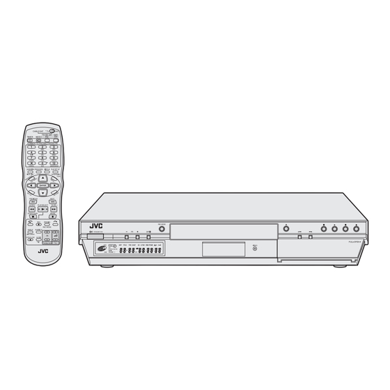
DVD VIDEO RECORDER
DR-M1SL
for ver.B
Since the whole mechanism assembly unit is replaced, the DVD recorder
mechanism of this unit need not be adjusted.
TABLE OF CONTENTS
Area Suffix
B -------------------------- U.K.
E ------ Continental Europe
EF -------------------- France
for ver.E,EF
No.XA013
2003/11
Advertisement

Related Manuals for JVC DR-M1SL


Summary of Contents for JVC DR-M1SL
-
Page 1: Table Of Contents
SERVICE MANUAL DVD VIDEO RECORDER XA013 2003 DR-M1SL Area Suffix B -------------------------- U.K. E ------ Continental Europe EF -------------------- France for ver.B for ver.E,EF Since the whole mechanism assembly unit is replaced, the DVD recorder mechanism of this unit need not be adjusted. - Page 2 SPECIFICATION GENERAL Power requirement AC 220 V - 240 Vd, 50 Hz/60 Hz Power consumption Power on : 34 W Power off : 18.5 W Temperature Operating : 5°C to 40°C Storage : -20°C to 60°C Operating position Horizontal only Dimensions (W ×...
-
Page 3: Precaution
SECTION 1 PRECAUTION Safety Precautions (1) This design of this product contains special hardware and voltmeter. many circuits and components specially for safety purpos- Move the resistor connection to each exposed metal es. For continued protection, no changes should be made part, particularly any exposed metal part having a return to the original design unless authorized in writing by the path to the chassis, and measure the AC voltage across... - Page 4 Important for laser products 5.CAUTION : If safety switches malfunction, the laser is able 1.CLASS 1 LASER PRODUCT to function. 2.DANGER : Invisible laser radiation when open and inter 6.CAUTION : Use of controls, adjustments or performance of lock failed or defeated. Avoid direct exposure to beam. procedures other than those specified herein may result in 3.CAUTION : There are no serviceable parts inside the hazardous radiation exposure.
-
Page 5: Specific Service Instructions
SECTION 2 SPECIFIC SERVICE INSTRUCTIONS This service manual does not describe SPECIFIC SERVICE INSTRUCTIONS. (No.XA013)1-5... -
Page 6: Disassembly
SECTION 3 DISASSEMBLY Main body section 3.1.1 Remove the top cover (See figure 1) (1) Remove the four screws A attaching the top cover on both sides of the main body. (2) Remove the five screws B attaching the top cover on the Top cover Top cover back of the main body. - Page 7 3.1.3 Remove the mechanism assembly (See figure 4) Mechanism assembly • Prior to performing the following procedure, remove the top Module board cover. • There is no need to remove the front panel assembly. (1) Disconnect the socket wire from connector CN5303 on the power supply board.
- Page 8 3.1.5 Remove the power supply board (See figure 7) Fastener Power supply board CN5303 • Prior to performing the following procedure, remove the top cover. (1) Disconnect the wire from connector CN5301, CN5302, CN5303, CN5305, CN5001 on the power supply board. Fastener Fastener (2) Remove the two screws F attaching the power supply...
-
Page 9: Adjustment
SECTION 4 ADJUSTMENT Timer clock adjustment (for only ver.E) If an error comes to arise for a clock, the following procedure will adjust. Signal (A1) No signal Mode Equipment Frequency counter Measuring point (D1) IC3001 pin 61 (D2) IC3001 pin 17 (D3) C3026 + and - Adjustment part... -
Page 10: Troubleshooting
Data code When the main body is set to JIG mode and when the main body is under JIG mode, the remote control unit attached to DR-M1SL operates only in "Remote Control Code 1". Since DR-M1SL is in "Remote Control Code 3" when it is shipped and just after its batteries are changed, "Remote Control Code 3"... - Page 11 (1) Turn the main body ON. (2) Press the buttons of the remote control unit attached to DR-M1SL in the following order : "SET UP" → "2" → "8" → "ENTER" (3) When a colon ":" between "hour" and "time" of a clock in FL indicator disappears, it means that the main body has been set to JIG mode properly.
- Page 12 (3) SYSTEM INFO menu is displayed in the television screen. (4) To move cursor in SYSTEM INFO, use the " ", " ", " ", and " " buttons of a remote control unit attached to DR-M1SL. < VERSION >...
- Page 13 5.1.5 Taking out a disc A disc can be taken out manually even when the main body is turned off. (1) Open the front door. (2) Pass a thin wire through a hole in the DVD recorder mechanism unit. (3) The disc tray comes out slightly. Take out the disc tray manually. DVD recorder mechanism unit Front door Hole...
- Page 14 SCHEMATIC DIAGRAMS DVD VIDEO RECORDER DR-M1SL CD-ROM No.SML200311 Area Suffix B -------------------------- U.K. E ------ Continental Europe EF -------------------- France for ver.B for ver.E,EF Since the whole mechanism assembly unit is replaced, the DVD recorder mechanism of this unit need not be adjusted.
- Page 15 In regard with component parts appearing on the silk-screen printed side (parts side) of the PWB diagrams, the parts that are printed over with black such as the resistor ( diode ( ) and ICP ( ) or identified by the " " mark nearby are critical for safety. When replacing them, be sure to use the parts of the same type and rating as specified by the manufacturer.
- Page 16 Wiring diagram BB[AL5V] NC[GND] BB[AL5V] AUDIO_IN AUDIO_IN AUDIO_IN AUDIO_IN MOD_SDA CH_SW MOD_SDA CH_SW CN6202 CN6201 MOD_B[AL5V] MOD_B[SW5V] MOD_B[AL5V] MOD_B[SW5V] DET_OUT DET_OUT MOD_SCL CONV.CTL[H] MOD_SCL CONV.CTL[H] BIT_GND BIT_GND VIDEO_IN VIDEO_IN VIDEO_IN VIDEO_IN BIT_OUT BIT_OUT NC[GND] TU[30V] DET_GND DET_GND RF_AGC [RF_AGC] RF_AGC [RF_AGC] DET_IN DET_IN...
- Page 17 Block diagrams DIGITAL 0 2 J4112 IEEE1394 TPA+ TPA- TPB+ TPB- IEEE1394 controller terminal PHY_RESET[L] IC1801 PHY_LREQ PHY_CLK PHY_CNA PHY_CTL[0],[1] PHY_DATA[0-7] PHY_LPS CIN VYIN SYNCDET CROUT CBOUT PHY_LINK_ON Video TO CN4101 YVOUT COUT RYOUT RCOUT controller IEEE1394 section (SHEET 2) SHEET 10 IC1001 SYS_RESET[L]...
- Page 18 MAIN 0 3 RCOUT COUT 480I[H] RYOUT YVOUT CBOUT CROUT AO_FSYNC AO_D[0] DAC_RST[L] AO_SCLK A_DAC_CS AO_MCLKO TO CN1001 DAC_SCL AI_D[0] DAC_SDA A_MUTE2[H] AO_IEC958 Audio signal control section (SHEET 8) SHEET 5 YTODIGI CTODIGI SYNC_DET K_BUS_REQ K_BUS_OUT K_BUS_CLK K_BUS_IN SYS_RESET[L] P_MUTE[H] P_CTL[H] SYNC_DET VD TO SHEET 11 AUDIO_OUT1[L/R] J4109...
- Page 19 SW.REG 0 1 D2.5V 2.5V REG. IC5305 TO CN5102 AC-DC MAIN AC IN D1.8V D5001 1.8V REG. P.SAVE[L] IC5302 TO CN5101 Switching 3.3V REG. V3.3V Power MAIN regurator IC5303 transformer IC5101 D5.0V T5001 5V REG. IC5304 TO DVD Recorder unit DC5V DV12V TO Fan assembly Power supply section (SHEET 1)
- Page 20 Standard schematic diagrams Power supply section B5501 Q5310 D5201 CP5301 R5310 2SD2144S/UV/ 10ELS4 1.5A /125 2SC3576 ERA18-02 C5201 /6.3 L5207 D5213 RK14 Parts are safety assurance parts. IC5305 SI-3012KM C5210 C5318 When replacing those parts make /6.3 sure to use the specified one. ON/OFF Vout L5201...
- Page 21 IEEE1394 section D3.3V C1806 C1805 L1802 L1801 C1804 C1803 /6.3 /6.3 C1814 C1813 OPEN OPEN R1820 C1810 OPEN K1801 X1801 NAX0551-001X SHORT TSB41AB2PAP IC1801 TO SHEET 4 PHY_RESET[L] PHY_LREQ LREQ AGND R1801 0‘ PHY_CLK SYSCLK R1802 0‘ PHY_CNA PHY_CTL[0] CTL0 PHY_CTL[1] CTL1 PHY_DATA[0-7]...
- Page 22 DDR SDRAM section IC1603 IC1603 IC1603 IC1603 IC1603 IC1603 IC1603 IC1603 IC1604 IC1604 IC1604 IC1604 IC1604 IC1604 IC1604 IC1604 HY5DU281622DT-6 HY5DU281622DT-6 HY5DU281622DT-6 HY5DU281622DT-6 HY5DU281622DT-6 HY5DU281622DT-6 HY5DU281622DT-6 HY5DU281622DT-6 HY5DU281622DT-6 HY5DU281622DT-6 HY5DU281622DT-6 HY5DU281622DT-6 HY5DU281622DT-6 HY5DU281622DT-6 HY5DU281622DT-6 HY5DU281622DT-6 SSTL2_VDD DDR_A[0] DDR_DQ[0] DDR_A[0] DDR_DQ[16] SDRAM_DQ[0] SDRAM_DQ[0] DDR_DQ[0]...
- Page 23 TO SHEET 3 Media processor section D3.3V SDRAM_A[0-15] SDRAM_DQ[16-31] SDRAM_DQ[0-15] ATA_DAT[0-15] ATA_DAT[0-15] C1402 C1401 OPEN OPEN IC1401 IC1401 IC1401 IC1401 IC1401 IC1401 IC1401 IC1401 IC1401 IC1401 DMN8600-C0 DMN8600-C0 DMN8600-C0 DMN8600-C0 DMN8600-C0 DMN8600-C0 DMN8600-C0 DMN8600-C0 DMN8600-C0 DMN8600-C0 IC1402 OPEN R1401 ATA_RESET B1401 R1402 ATA_DMARQ...
- Page 24 Video signal controller section C1099 C1100 VDDI1.8 IC1002 DIGI3.3V HY57V161610DTC8 K4S161622D-TC80 D2.5V C1042 SHEET 4 D1.8V DQ15 DQ15 TO SHEET 6 P_CTL[H] DQ14 RA1002 RA1003 DQ14 SYS_RESET[L] VSSQ VSSQ R1036 K_BUS_IN DQ13 DQ13 K_BUS_CLK DQ12 R1035 C1043 DQ12 C1047 SHEET 4 K_BUS_OUT Q1002 VDDQ...
- Page 25 ATAPI Interface section IC2201 SN74CBTD6210G CN2201 QGF0533F1-4 R2204 K2201 RSTATA ATA_DAT[7] RA2201 ATA_DAT[8] FE_DAT[7] FE_DAT[7] K2202 HD_AT[7] ATA_DAT[6] FE_DAT[8] FE_DAT[8] K2203 HD_AT[8] ATA_DAT[9] FE_DAT[6] FE_DAT[6] K2204 HD_AT[6] ATA_DAT[5] FE_DAT[9] FE_DAT[9] K2205 HD_AT[9] FE_DAT[5] K2206 HD_AT[5] ATA_DAT[10] FE_DAT[5] FE_DAT[10] K2207 HD_AT[10] ATA_DAT[4] FE_DAT[10] FE_DAT[4]...
- Page 26 FLASH-ROM section D3.3V IC2001 MBPL65LM90TN K2001 SHORT LH_AR[16] LH_AR[17] LH_AR[15] F_PROT[H] VCCQ R2009 LH_AR[22] LH_AR[14] MADD[22] LH_AR[13] MADD[21] C2002 SHEET 4 DQ15 MADD[6-21] MADD[6-21] LH_AR[12] MADD[13] /MDT[0-15] LH_AR[11] MADD[20] DQ14 MADD[21] LH_AR[10] MADD[12] C2001 MADD[20] B2102 B2101 LH_AR[9] MADD[19] /6.3 DQ13 MADD[19] LH_AR[22]...
- Page 27 Audio signal control section K8202 ADC_RST[L] R8233 4.7‘ R8232 I2C_CLK2 R8231 SHEET 12 I2C_DATA2 C8214 Q8201 A_MUTE1[H] UMH2N /6.3 R8234 R8220 Q8202 4.7k UMD3N C8213 _0.5% R8218 C8208 R8222 _0.5% 470p 4.3k R8223 SHEET 11 _0.5% C8206 4700p R8221 R8251 IC8002 C8005 AUDIO_OUT1[R]...
- Page 28 Audio/Video signal input control section C4318 CN4301 C4319 CN4302 470p C/R1 R4319 C4310 470p C/R2 R4311 D4301 L4301 1SS133 R4317 R4318 IC4301 LA7357M C4306 R4306 0.01 1.2k R4312 Q4301 0‘ IC4304 R4307 R4304 74HC4538D C4308 C4307 0.01 0.01 FSC_IN C4302 C4301 C4304 Q4302...
- Page 29 Input/output relay section TO CN1001 SHEET 5 AO_FSYNC AO_D[0] DAC_RST[L] AO_SCLK A_DAC_CS AO_MCLKO DAC_SCL SHEET 8 AI_D[0] DAC_SDA A_MUTE2[H] AO_IEC958 K_BUS_REQ K_BUS_OUT K_BUS_CLK K_BUS_IN SYS_RESET[L] CROUT P.MUTE[H] CBOUT B4101 SHORT P_CTL[H] YVOUT SHEET 11 SHEET 12 RYOUT SYNC_DET 480I[L] SAT_CTL CTODIGI R.PAUSE YTODIGI...
- Page 30 Input/output terminal section J7309 J7309 Pr_OUT Pb_OUT Y_OUT 4_3[H] 16_9[H] SHEET 12 R7307 Q7301 Q7302 R7339 R7308 R7340 R7301 Q7303 Q7310 1/4W R7303 SHEET 12 4.7k D7301 Q7312 R7305 R7341 UN521E-X DTC144WUA-X P50_I/O MTZJ2.7B-T2 PDTC144WU-X RD2.7ES/B2/-T2 RN1309-X SCR_ID Q7311 R7309 R7302 BIAS/RGB_CTL R7304...
- Page 31 System controller section TO SHEET 11 SCR_ID SEPA_IN[H] TO SHEET 9 SECAM[H] 4_3[H] 16_9[H] RGB_TH[H] AV1_YC_IN[H] BIAS/RGB_CTL TO SHEET 11 AV1_L AV1_L AV2_H AV2_H P.MUTE[H] ADC_RST[L] RAPID_SW A_MUTE1[H] V_MUTE[L] TO SHEET 8 I2C_DATA_A/V TO SHEET 9 I2C_CLK_A/V C3032 R3001 SVss HDD_LED R3083 R3004...
- Page 32 Tuner section TU6001 L6002 RF5V TO SHEET 1 SW5V L6005 SW12V L6701 3.3^ C6751 C6752 /6.3 OPEN TU_AUDIO[L] TO SHEET 8 TU_AUDIO[R] K6706 C6718 OPEN C6715 C6717 R6716 R6714 R6712 L6702 3.3^ R6720 5.6k R6711 470k C6719 C6713 0.22 CAPL_M RESETQ TU6001 D6701...
- Page 33 FL Display and operation switch section D7112 S7132 D7113 S7023 S7022 S7021 REC_MODE OPERATION S7133 S7113 S7001 S7002 D7114 REC-LINK S7134 S7114 IC7002 GP1UM261XK PNA4652M00XB D7115 V.OUT R7016 S7135 S7115 SHORT C7001 C7008 /6.3 C7006 /6.3 R7009 OPEN R7142 R7015 R7005 4.7k Q7101...
- Page 34 Printed circuit boards Main board KA4102 IC4304 R4317 R6708 C6032 C6037 B4124 R4311 R6710 K4106 B4123 R6020 R4318 R6709 R6033 R6021 TU6001 X6701 C6753 K6705 C6707 R4319 K6702 L6702 B4122 D4301 K6701 KA4101 CN4302 R6707 C6006 C6008 C6014 C6715 B4121 C6706 R6712 K4105...
- Page 35 Power supply board FL Display board S7023 VA5003 FC5002 FC5001 C7012 C5003 F5001 CN7001 S7021 S7002 S7001 S7022 C5103 IC7002 C5107 D5106 C5108 R5104 C5004 C5101 W404 R7003 C5105 W403 C5104 IC5101 W201 C5102 D7034 D7021 C7005 C5109 C7004 R7010 D7032 C5106 R7053...
- Page 36 DVD Digital board Forward side Reverse side ZP1002 ZP1006 ZP1062 ZP1078 CN1401 ZP1004 ZP1036 ZP1064 C1420 CN1001 ZP1003 ZP1007 ZP1035 ZP1039 ZP1063 ZP1005 TL1029 ZP1037 ZP1061 ZP1065 ZP1077 C1100 ZP1088 ZP1089 K2208 K2207 K2210 K2209 ZP1087 ZP1091 ZP1093 K2204 K2205 K2212 K2211 ZP1090...
- Page 37 << MEMO >> << MEMO >> 2-24 (No.XA013SCH)
- Page 38 << MEMO >> (No.XA013SCH) 2-3 2-25...
- Page 39 PARTS LIST [DR-M1SL] * All printed circuit boards and its assemblies are not available as service parts. * (x_) in a description column shows the number of the used part. Area Suffix B -------------------------- U.K. E ------ Continental Europe EF -------------------- France...
- Page 40 Exploded view of general assembly and parts list Block No.M1MM COAXIAL OUT BOARD ASSY<94> AV OUT BOARD ASSY<29> DIGITAL BOARD ASSY<02> MAIN BOARD ASSY<03> Insert the bushing of POWER CORD so as not to twist the cord. Inserts to C1802. FRONT BOARD ASSY<28>...
- Page 41 General assembly Block No. [M][1][M][M] Symbol No. Part No. Part Name Description Local LP10483-003F FRONT PANEL ASSY M1SLB LP10483-002F FRONT PANEL ASSY M1SLE LP10483-004F FRONT PANEL ASSY M1SLEF LP31228-001A DOOR(JACK) LP31229-003A WINDOW(DOOR) M1SLB LP31229-002A WINDOW(DOOR) M1SLE LP31229-004A WINDOW(DOOR) M1SLEF PU60109 CATCHER LP30002-0E1A...
- Page 42 MTZJ27C-T2 Z DIODE Q5308 2SD1858/QR/-T TRANSISTOR D5307 or RD27ES/B3/-T2 Z DIODE Q5310 2SD2144S/UV/-T TRANSISTOR D5309 RK34-LFB2 SB DIODE Q5310 or 2SC3576-JVC-T TRANSISTOR D5310 RK34-LFB2 SB DIODE Q5311 UMD12N-W DIGI TRANSISTOR D5311 RK34-LFB2 SB DIODE Q5311 or XP4313-W DIGI TRANSISTOR PC5101...
- Page 43 Symbol No. Symbol No. Part No. Part Name Description Local Part No. Part Name Description Local R5104 NRSA63J-102X MG RESISTOR 1kΩ 1/16W J IC1406 SN74HCT08APW-X IC R5105 QRE141J-680Y C RESISTOR 68Ω 1/4W J IC1407 SN74LV08APW-X IC R5106 NRSA63J-392X MG RESISTOR 3.9kΩ...
- Page 44 Symbol No. Symbol No. Part No. Part Name Description Local Part No. Part Name Description Local C1027 NCB31CK-104X C CAPACITOR 0.1uF 16V K C1450 NCB31CK-104X C CAPACITOR 0.1uF 16V K C1028 NCB31CK-104X C CAPACITOR 0.1uF 16V K C1451 NCB31CK-104X C CAPACITOR 0.1uF 16V K...
- Page 45 Symbol No. Symbol No. Part No. Part Name Description Local Part No. Part Name Description Local C1705 NCB31CK-104X C CAPACITOR 0.1uF 16V K R1069 NRSA63D-222X MG RESISTOR 2.2kΩ 1/16W D C1706 NCB31CK-104X C CAPACITOR 0.1uF 16V K R1070 NRSA63D-122X MG RESISTOR 1.2kΩ...
- Page 46 Symbol No. Symbol No. Part No. Part Name Description Local Part No. Part Name Description Local R1618 NRSA63J-270X MG RESISTOR 27Ω 1/16W J RA1601 NRZ0040-101X NET RESISTOR 100Ω 1/16W J x4 R1619 NRSA63J-101X MG RESISTOR 100Ω 1/16W J RA1602 NRZ0040-101X NET RESISTOR 100Ω...
- Page 47 Symbol No. Symbol No. Part No. Part Name Description Local Part No. Part Name Description Local K1018 NQR0129-002X FERRITE BEADS IC4301 LA7357M-W M1SLEF K1019 NRSA02J-0R0X MG RESISTOR 0Ω 1/10W J IC4304 74HC4538D-X M1SLEF K1401 NRSA63J-0R0X MG RESISTOR 0Ω 1/16W J IC6701 MSP3417GQGB8V3X IC K1402...
- Page 48 Symbol No. Symbol No. Part No. Part Name Description Local Part No. Part Name Description Local Q7305 or DTC144WUA-X DIGI TRANSISTOR D7113 or 1SS270A-T2 SI DIODE Q7305 or PDTC144WU-X DIGI TRANSISTOR D7114 1SS133-T2 DIODE Q7305 or RN1309-X DIGI TRANSISTOR D7114 or 1SS270A-T2 SI DIODE...
- Page 49 Symbol No. Symbol No. Part No. Part Name Description Local Part No. Part Name Description Local C4071 QCFB1HZ-104Y C CAPACITOR 0.1uF 50V Z C7340 QETN0JM-477Z E CAPACITOR 470uF 6.3V M C4072 QEKJ0JM-107Z E CAPACITOR 100uF 6.3V M C7345 NCB31EK-103X C CAPACITOR 0.01uF 25V K...
- Page 50 Symbol No. Symbol No. Part No. Part Name Description Local Part No. Part Name Description Local R3022 NRSA63J-0R0X MG RESISTOR 0Ω 1/16W J R4036 NRSA63J-750X MG RESISTOR 75Ω 1/16W J R3025 NRSA63J-0R0X MG RESISTOR 0Ω 1/16W J R4037 NRSA63J-101X MG RESISTOR 100Ω...
- Page 51 Symbol No. Symbol No. Part No. Part Name Description Local Part No. Part Name Description Local R7338 NRSA63J-101X MG RESISTOR 100Ω 1/16W J R8251 NRSA63J-101X MG RESISTOR 100Ω 1/16W J R7339 QRE141J-101Y C RESISTOR 100Ω 1/4W J R8252 NRSA63J-682X MG RESISTOR 6.8kΩ...
- Page 52 Symbol No. Symbol No. Part No. Part Name Description Local Part No. Part Name Description Local K6704 NQR0200-003X FERRITE BEADS Q7001 DTA114ESA-T DIGI TRANSISTOR K6705 NQR0200-003X FERRITE BEADS K6706 NQR0200-003X FERRITE BEADS D7001 1SS133-T2 DIODE K6707 NQR0200-003X FERRITE BEADS M1SLEF D7001 or 1SS270A-T2...
- Page 53 Coax out board Block No. [9][4] Symbol No. Part No. Part Name Description Local LPA10201-02A3 COAX OUT BOARD ASSY IC8501 74VHCT08ASJ-X IC 2-input AND gate C8501 QETN1CM-107Z E CAPACITOR 100uF 16V M C8502 NCB31CK-104X C CAPACITOR 0.1uF 16V K C8503 QETN1HM-475Z E CAPACITOR 4.7uF 50V M...
- Page 54 Packing materials and accessories parts list Block No.M2MM ADHESIVE TAPE FINAL ASSY<M1> SPEC OF BARCODE 3-16(No.XA013)
- Page 55 Packing and accessories Block No. [M][2][M][M] Symbol No. Part No. Part Name Description Local LP31277-001B PACKING CASE LP10496-001A CUSHION(L) LP10497-001A CUSHION(R) PQM30021-93 POLY BAG PEAC0300-02 RF CABLE QAL0517-005 LED CABLE ASSY R6PRPA-2ST BATTERY (x2) QPC02202230P POLY BAG 22cm x 22cm ...
- Page 56 VICTOR COMPANY OF JAPAN, LIMITED AV & MULTIMEDIA COMPANY OPTICAL DISC CATEGORY 1644, Shimotsuruma, Yamato, Kanagawa 242-8514, Japan (No.XA013) Printed in Japan...