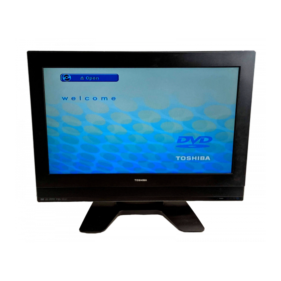
Toshiba 23HLV87 Circuit Diagrams
Hide thumbs
Also See for 23HLV87:
- Owner's manual (80 pages) ,
- Circuit diagrams (32 pages) ,
- Service manual (77 pages)
Advertisement
Quick Links
All manuals and user guides at all-guides.com
FILE NO. 810-200728GR
REVISED: 01
CIRCUIT DIAGRAMS
LCD TV/DVD COMBINATION
23HLV87
l
The above model is classified as a green product (*1), as indicated by the underlined serial number.
This Service Manual describes replacement parts for the green product. When repairing this green
product, use the part(s) described in this manual and lead-free solder (*2).
For (*1) and (*2), see the next page.
DOCUMENT CREATED IN JAPAN, March, 2007 GREEN
Advertisement

Summary of Contents for Toshiba 23HLV87
- Page 1 REVISED: 01 CIRCUIT DIAGRAMS LCD TV/DVD COMBINATION 23HLV87 The above model is classified as a green product (*1), as indicated by the underlined serial number. This Service Manual describes replacement parts for the green product. When repairing this green product, use the part(s) described in this manual and lead-free solder (*2).
- Page 2 All manuals and user guides at all-guides.com DVD BLOCK DIAGRAM LCD BLOCK DVD LOADER SL260WRA 3.3V, 1.8V DVD/CDPD DVD_MENU RF_A, B, C, D, E, F DVD_TRIP STB_DVD VIDEO DVD/CD, DVD_LD, CD_LD DVD PB/C DVD PB/Y V1P4/FMO/FOO DVD_RMC TR+/-, F+/- Motor Drive TRO/STBY/DMO SPINDLE/ MPEG/MICON/DSP/RF_AMP...
- Page 3 All manuals and user guides at all-guides.com SCALER/LVDS/ADC/JACK/AV SWITCH/STEREO/SOUND AMP BLOCK DIAGRAM T SDA T SCC M_SDA SDRAM DEMUX TUNER M_SCC S5H1409 DTVS205CH201 SDRAM CVBS AV1_S_VIDE_C SDRAM AV1_S_VIDE_Y AV1_CVBS TV VIDEO DECORD AV1_L /ADC/SCALE AV1_R FLASH MSD116L AV2_CVBS AV2_L AV2_R L OUT L OUT AV3_Y...
- Page 4 All manuals and user guides at all-guides.com POWER BLOCK DIAGRAM P O W E R S U P P L Y L C D A P N E L M A I N P C B 5 VA U 1 0 1 2 VA 2 .
- Page 5 All manuals and user guides at all-guides.com PRINTED CIRCUIT BOARDS MAIN (TOP SIDE) MAIN (BOTTOM SIDE)
- Page 6 All manuals and user guides at all-guides.com PRINTED CIRCUIT BOARDS OPERATION (TOP SIDE) OPERATION (BOTTOM SIDE) INPUT (TOP SIDE) INPUT (BOTTOM SIDE) REMOCON (TOP SIDE) REMOCON (BOTTOM SIDE)
- Page 7 All manuals and user guides at all-guides.com PRINTED CIRCUIT BOARDS DECODER (TOP SIDE) DECODER (BOTTOM SIDE)
- Page 8 All manuals and user guides at all-guides.com PRINTED CIRCUIT BOARDS POWER (TOP SIDE) POWER (BOTTOM SIDE)
- Page 9 All manuals and user guides at all-guides.com MSD116L SCHEMATIC DIAGRAM (MAIN PCB) t i b t i b...
- Page 10 All manuals and user guides at all-guides.com MSD116L POWER SCHEMATIC DIAGRAM (MAIN PCB)
- Page 11 All manuals and user guides at all-guides.com SYS POWER SCHEMATIC DIAGRAM (MAIN PCB)
- Page 12 All manuals and user guides at all-guides.com MCU & RTC SCHEMATIC DIAGRAM (MAIN PCB)
- Page 13 All manuals and user guides at all-guides.com DEMODULATOR SCHEMATIC DIAGRAM (MAIN PCB) H-10...
- Page 14 All manuals and user guides at all-guides.com SDRAM SCHEMATIC DIAGRAM (MAIN PCB) t i b t i b t i b t i b t i b t i b H-11 H-12...
- Page 15 All manuals and user guides at all-guides.com AUDIO SCHEMATIC DIAGRAM (MAIN PCB) H-13 H-14...
- Page 16 All manuals and user guides at all-guides.com TUNER SCHEMATIC DIAGRAM (MAIN PCB) ) - ( H-15 H-16...
- Page 17 All manuals and user guides at all-guides.com AV INPUT & OUTPUT SCHEMATIC DIAGRAM (MAIN PCB) H-17 H-18...
- Page 18 All manuals and user guides at all-guides.com YPBPR & VGA SCHEMATIC DIAGRAM (MAIN PCB) H-19 H-20...
- Page 19 All manuals and user guides at all-guides.com HDMI SCHEMATIC DIAGRAM (MAIN PCB) 9 J9 J H-21 H-22...
- Page 20 All manuals and user guides at all-guides.com EXT-MODULE CON SCHEMATIC DIAGRAM (MAIN PCB) H-23 H-24...
- Page 21 All manuals and user guides at all-guides.com VADDIS & SDRAM FLASH SCHEMATIC DIAGRAM (DECODER PCB) < l e t < : t i : t i t i b t i b < < H-25 H-26...
- Page 22 All manuals and user guides at all-guides.com POWER SUPPLY SCHEMATIC DIAGRAM (DECODER PCB) H-27 H-28...
- Page 23 All manuals and user guides at all-guides.com AV INPUT & OUTPUT SCHEMATIC DIAGRAM (DECODER PCB) H-29 H-30...
- Page 24 All manuals and user guides at all-guides.com FE REGULATOR SCHEMATIC DIAGRAM (DECODER PCB) : l o : 0 . : 0 . & & H-31 H-32...
- Page 25 All manuals and user guides at all-guides.com PFC SCHEMATIC DIAGRAM (POWER PCB) H-33 H-34...
- Page 26 All manuals and user guides at all-guides.com PWM SCHEMATIC DIAGRAM (POWER PCB) H-35 H-36...
- Page 27 All manuals and user guides at all-guides.com INTERCONNECTION DIAGRAM B-ON B-ON B-ADJ B-ADJ AC120~240V 50/60Hz POWER PCB +24V +24V LOAD- LOAD- +24V +24V LOAD+ +24V +24V LOAD+ +24V +24V SLOT IN DVD +24V +24V DRIVE 12V/3V 12V/3V 12V/3V LIMIT LIMIT OPTICAL PICK-UP TRYIN TRYIN...
- Page 28 All manuals and user guides at all-guides.com WAVEFORMS AV SWITCH2 100µs 2.0ms 20ns 2.0V 500mV 1.0V SOUND AMP/HEADPHON AMP MICON 2.0ms 100µs 50ns 500mV 2.0V 500mV SCALER 2.0ms 20µs 20µs 500mV 500mV 500mV TUNER 20µs 2.0ms 20µs 500mV 500mV 2.0V STEREO 2.0ms 20µs...
- Page 29 All manuals and user guides at all-guides.com WAVEFORMS 5µs 20µs 5µs 500mV 200mV 2.0V LVDS 20µs 10ms 5µs 200mV 100mV 500mV JACK INTERFACE_HDMI IC 1.0ms 20µs 20µs 1.0V 200mV 1.0V 1.0ms 20µs 20µs 1.0V 1.0V 500mV 20µs 10µs 5µs 1.0V 2.0V 500mV The following waveforms were measured at the point of the corresponding...
- Page 30 All manuals and user guides at all-guides.com WAVEFORMS AUDIO/VIDEO MPEG/MICON/DSP 2µs 500µs 10ns 2.0V 500mV 100mV 500µs 500mV 20mV 10µs 20ns 200mV 1.0V 10µs 200ns 200mV 1.0V MEMORY REGULATOR 2 2µs 2.0V 500mV The following waveforms were measured at the point of the corresponding NOTE: balloon number in the schematic diagram.
- Page 31 All manuals and user guides at all-guides.com TOSHIBA CORPORATION 1-1, SHIBAURA 1-CHOME, MINATO-KU, TOKYO 105-8001, JAPAN...


