Advertisement
Quick Links
TV BAR
Service
Service
Service
Service Manual
©
Copyright 2014 WOOX Innovations limited.
All rights reserved. No part of this publication may be reproduced, stored in a retrieval system or
transmitted, in any form or by any means, electronic, mechanical, photocopying, or otherwise
without the prior permission of WOOX Innovations. Philips and the Philips' shield Emblem are
registered trademarks of Koninklijke Philips N.V. and are used by WOOX Innovations Limited
under license from Koninklijke Philips N.V.
Published by
SW_HF1402
Version 1.0
All manuals and user guides at all-guides.com
1 - 1
TABLE OF CONTENTS
Location Of PCBA & Versions Variation.................... 1-2
Technical Specification .............................................. 1-3
Safety instruction ...................................................... 1-4
Software upgrade instruction ........................................ 2
Trouble Shooting............................................................ 3
Dismantling instructions ................................................ 4
Block Diagram................................................................ 5
Wiring Diagram .............................................................. 6
MAIN+MP3&USB+SPK+VFD&BT+AUX&OPTICAL PCB
WIRELESS PCB(Main unit) .......................................... 8
AMP+LED PCB(Subwoofer) .......................................... 9
POWER PCB(Subwoofer) .......................................... 10
Mechanical Exploded .................................................. 11
Revision List ................................................................ 12
Chapter
(Main unit) .......... 7
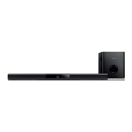
HTL3110B/F7
GB
3140 038 61420
PHILIPS
Advertisement

Related Manuals for Philips HTL3110B/F7


Summary of Contents for Philips HTL3110B/F7
- Page 1 WOOX Innovations. Philips and the Philips’ shield Emblem are registered trademarks of Koninklijke Philips N.V. and are used by WOOX Innovations Limited under license from Koninklijke Philips N.V.
- Page 2 All manuals and user guides at all-guides.com 1 - 2 LOCATION OF PCBA USB PCB AUX PCB SPK_R PCB SPK_L PCB WIRELESS PCB TOUCH PCB NFC PCB VFD PCB MAIN PCB Main Unit Wireless TX module MAIN PCB LED PCB POWER PCB Subwoofer VERSIONS VARIATION:...
- Page 3 • RMS Total output power: 120W RMS (+/- • Power supply: 0.5 dB, 10% THD) • Model (Philips AC power adapter): • Frequency response: 20 Hz-20 kHz / ±3 DYS602-210309W; AS650-210-AA309 • Input: 100-240 V~, 50/60 Hz 1.5 A •...
- Page 4 Unplug this apparatus during lightning storm or when unused for long periods of Your product is designed and manufactured with high quality materials and components, time. which can be recycled and reused. Please visit www.recycle.philips.com for additional • Refer all servicing to service personnel.
- Page 5 < TREBLE -, BASS- and - (Volume) > on the remote control. 3) Software Upgrade via USB a) Check the latest software version on www.philips.com/support. • Search for your model and click on“Software and drivers”.
- Page 6 All manuals and user guides at all-guides.com 3 - 1 3 - 1 Trouble Shooting(main unit) MAIN UNIT REPAIR CHART 1/2 Power Supply All Function Standby LED Didn't power ON AUX IN Wireless optical&COAXIAL IN Audio line IN Bluetooth No Output HDMI ARC No Sound red light is not bright...
- Page 7 All manuals and user guides at all-guides.com 3 - 2 3 - 2 Trouble Shooting(main unit) MAIN UNIT REPAIR CHART 2/2 Audio line IN Bluetooth Wireless No Output No Output No Output No Output Check JK305 Check BT401 Check Q404 R419 L403 Check MD401 Check CN302 RB302 Check L401 L402 and...
- Page 8 All manuals and user guides at all-guides.com 3 - 3 3 - 3 Trouble Shooting(subwoofer) IC401 and IC501 8pin Check power D905,D910,IC901, BK3.3V IC902, Q902,Transformer and their conjoint part D905, IC901, IC906 L202, L203 Change transmitter module...
- Page 9 All manuals and user guides at all-guides.com 4- 1 4 - 1 Note:In some service positions the components or copper patterns of one board may risk touching its Dismantling of the VFD+BT Boards 1) Loosen 2 screws “F” on the top of VFD+BT board as shown in fi gure 7. neighbouring pc boards or metallic parts.
- Page 10 All manuals and user guides at all-guides.com 4 - 2 4 - 2 Dismantling of the WIRELESS Boards assembly Dismantling Instructions(SUBWOOFER) 1) Loosen 1 screws “J” on the top of WIRELESS Board as shown in fi gure 10. Dismantling of Back panel assembly 1) Loosen 8 screws “K”...
- Page 11 All manuals and user guides at all-guides.com 5 - 1 5 - 1 Block Diagram(main unit) 74HC04 2219M40 Optical Wireless CS5343 4052 Switch MPEG Dolby Digital DAMP 27MHz TAS5715 NFC- H1 MP3/WMA SDRAM decode BM84 FLASH Bluetooth EN25F16 v3.0, A2DP MT8307OQE Reset AVRCP...
- Page 12 All manuals and user guides at all-guides.com 5 - 2 5 - 2 Block Diagram(subwoofer)
- Page 13 All manuals and user guides at all-guides.com 6 - 1 WIRING Diagram(main unit)
- Page 14 All manuals and user guides at all-guides.com 6 - 2 6 - 2 WIRING Diagram(subwoofer)
- Page 15 All manuals and user guides at all-guides.com 7- 1 7 - 1 IC303 INTERNAL IC DIAGRAM - CD4052BM MAIN+MP3&USB+SPK+VFD&BT+AUX&OPTICAL BOARD TABLE OF CONTENTS Internal IC Diagram ................7-1 Circuit Diagram .................. 7-2 Component Layout_Top View ............7-3 IC302 INTERNAL IC DIAGRAM - CS5343-CZZ Component Layout_Bottom View ............
- Page 16 All manuals and user guides at all-guides.com 7 - 2 7 - 2 CIRCUIT DIAGRAM D201 1N4148 PL33 R201 BT_ON/OFF R217 SUB Speaker JACK PCB Board R559 R202 PLAY/PAUSE_STATE R218 C203 R203 PLAY/PAUSE_CONTROL R219 R509 C517 C518 RB501 JK501 R204 BT_NEXT R220 R205...
- Page 17 All manuals and user guides at all-guides.com 7- 3 7 - 3 COMPONENT LAYOUT_TOP View LFM110990-0001 20131125 REV:A O4.0 O4.0 C417 R422 R421 PIN2 BT-R LFM110998-0001 131125 REV:A bar code location BM84 BT-L 20131125 LFM110997-0001 REV:A RB405 RB301 DP101 TSDA R119 C118 C128 C124...
- Page 18 All manuals and user guides at all-guides.com 7 - 4 7 - 4 COMPONENT LAYOUT_Bottom View R112 IC102 C113 R104 C114 R107 R105 C115 Q402 Q401 R106 R108 R109 D401 C116 C409 R111 C104 C102 C126 R411 R110 R413 R412 STANDBY SOURCE VOL+...
- Page 19 All manuals and user guides at all-guides.com 8 - 1 8 - 1 WIRELESS BOARD TABLE OF CONTENTS Circuit Diagram .................. 8-2 Component Layout_Top View ............8-3 Component Layout_Bottom View ............8-4...
- Page 20 All manuals and user guides at all-guides.com 8 - 2 8 - 2 CIRCUIT DIAGRAM MD401 CN402 R401 TSD 2 DATA W_INT1 R402 R403 W_SCL R404 W_SDA LRCK standby R405 TSD 2 MUTE R406 MCLK R407 ID pairing RX Link TX Link WSCL R408...
- Page 21 All manuals and user guides at all-guides.com 8 - 3 8 - 3 Component Layout_Top View MD401 C408 R407 C406 CN403 R405 C407 R406 R408 CN402 R409 R425 R404 R403 R426 C405 C404 R402 L402 R401 C402 L401 C401 C422 C403...
- Page 22 All manuals and user guides at all-guides.com 8 - 4 8 - 4 Component Layout_Bottom View...
- Page 23 All manuals and user guides at all-guides.com 9 - 1 9 - 1 IC501 INTERNAL IC DIAGRAM - TAS5715PHRR AMP & LED BOARD TABLE OF CONTENTS Internal IC Diagram ................9-1 Circuit Diagram .................. 9-2 Component Layout_Top View ............9-3 Component Layout_Bottom View ............
- Page 24 All manuals and user guides at all-guides.com 9 - 2 9 - 2 CIRCUIT DIAGRAM +3.3V R525 C518 C520 C523 C521 C522 C517 C519 R523 R524 FB502 20V1 +23V +3.3V 100MHZ 470U/35V R522 L502 15UH/3A AVDD AVDD PGND_AB PGND_AB OUT_B POWER OFF MUTE C505 D501...
- Page 25 All manuals and user guides at all-guides.com 9 - 3 9 - 3 Component Layout_Top View LFM110940-0201 RESET 3.3V 3.3V PIN1...
- Page 26 All manuals and user guides at all-guides.com 9 - 4 9 - 4 Component Layout_Bottom View RESET 3.3V 3.3V PIN1...
- Page 27 All manuals and user guides at all-guides.com 10 - 1 10 - 1 IC903/904/909 INTERNAL IC DIAGRAM - AZ431AZ-A CATHODE POWER BOARD TABLE OF CONTENTS Internal IC Diagram ................10-1 ANODE Circuit Diagram ................. 10-2 Component Layout_Top View ............10-3 Component Layout_Bottom View ............
- Page 28 All manuals and user guides at all-guides.com 10 - 2 10 - 2 CIRCUIT DIAGRAM L-6uH-5A 330K 330K 330K 330K C937 L903 R912 R913 R914 R915 HVCC C934 D905 1000U 50V FMX-G22S R909 222P/630V C911 C936 R936-939 102P-500V VCC2 PR2007 R940 R04-220 R04-220...
- Page 29 All manuals and user guides at all-guides.com 10 - 3 10 - 3 Component Layout_Top View WARNING: FOR CONTINUED PROTECTION AGAINST RISK OF FIRE REPLACE WITH SAME TYPE FUSE. CN902 PIN1 P903 P901 C939 C905 IC909 J912 C907 BD901 J905 C932 T902 L903...
- Page 30 All manuals and user guides at all-guides.com 10 - 4 10 - 4 Component Layout_Bottom View C961 PIN1 R956 R951 C908 R948 R959 D908 C928 R945 D907 C940 C906 R954 R910 R949 C942 R953 R950 R911 R909 R955 R9014 R9013 R9012 R912 R9020...
- Page 31 All manuals and user guides at all-guides.com 11- 1 11- 1 Mechanical Exploded View(Main unit) Note:A1=8+10+17+19+20+26+30 Power Adapter Power Cord...
- Page 32 All manuals and user guides at all-guides.com 11- 2 11- 2 Mechanical Exploded View(subwoofer) SW14 SW13 SW12 SW11 SW10 Note:B1=SW11+SW13 Power Cord...
- Page 33 All manuals and user guides at all-guides.com 12- 1 REVISION LIST Version 1.0 *Initial release...