Table of Contents
Advertisement
Quick Links
TABLE OF CONTENTS
1 Safety Precautions----------------------------------------------- 3
1.1. General Guidelines---------------------------------------- 3
1.2. Before Repair and Adjustment ------------------------- 4
1.3. Protection Circuitry ---------------------------------------- 4
1.4. Caution For Fuse Replacement------------------------ 4
1.5. Safety Part Information----------------------------------- 5
2 Warning -------------------------------------------------------------- 6
to Electrostatically Sensitive (ES) Devices---------- 6
2.2. Precaution of Laser Diode (SL-NE5) ----------------- 7
3 Service Navigation ----------------------------------------------10
3.1. Service Information --------------------------------------10
3.2. Troubleshooting Guide ---------------------------------- 11
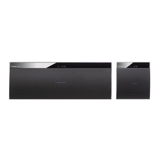
Wireless Speaker System
Model No.
Product Color: (K)...Black Type
PAGE
4 Specifications ---------------------------------------------------- 12
4.1. License ----------------------------------------------------- 13
5 General/Introduction------------------------------------------- 14
5.1. Using AirPlay with this system's speakers--------- 14
5.3. Bluetooth® Operations --------------------------------- 16
5.4. Playable media ------------------------------------------- 17
6 Location of Controls and Components------------------ 18
6.1. Main Unit Key Button Operations -------------------- 18
6.2. Remote Control Key Button Operations------------ 19
7 Installation Instructions -------------------------------------- 20
7.1. Connections ----------------------------------------------- 20
7.2. Inserting media ------------------------------------------- 21
7.3. Network settings------------------------------------------ 22
8 Service Mode ----------------------------------------------------- 25
© Panasonic Corporation 2013. All rights reserved.
Unauthorized copying and distribution is a violation of
law.
SL-NE5EF
SL-NE5EG
SB-NE5EF
SB-NE5EG
SC-NE5EF
SC-NE5EG
PSG1303005CE
PAGE
Advertisement
Table of Contents

Related Manuals for Panasonic SL-NE5EF


Summary of Contents for Panasonic SL-NE5EF
-
Page 1: Table Of Contents
3 Service Navigation ----------------------------------------------10 7.2. Inserting media ------------------------------------------- 21 3.1. Service Information --------------------------------------10 7.3. Network settings------------------------------------------ 22 3.2. Troubleshooting Guide ---------------------------------- 11 8 Service Mode ----------------------------------------------------- 25 © Panasonic Corporation 2013. All rights reserved. Unauthorized copying and distribution is a violation of law. - Page 2 8.1. Self Diagnostic Mode------------------------------------ 25 15.4. System Control (SB-NE5) ----------------------------- 94 8.2. Self Diagnostic Function Error Code ---------------- 26 15.5. Audio (SB-NE5) ------------------------------------------ 95 8.3. Doctor Mode Table (SB-NE5) ------------------------- 27 15.6. Power Supply (SB-NE5) ------------------------------- 96 8.4. Doctor Mode Table (SL-NE5) ------------------------- 31 16 Wiring Connection Diagram -------------------------------- 98 9 Service Fixture &...
-
Page 3: Safety Precautions
1 Safety Precautions 1.1. General Guidelines 1. IMPORTANT SAFETY NOTICE There are special components used in this equipment which are important for safety. These parts are marked by in the Schematic Diagrams, Circuit Board Layout, Exploded Views and Replacement Parts List. It is essential that these critical parts should be replaced with manufacturer’s specified parts to prevent X-RADIATION, shock, fire, or other hazards. -
Page 4: Before Repair And Adjustment
1.2. Before Repair and Adjustment SL-NE5 Disconnect AC power to discharge unit AC Capacitors (C1001, C1003, C1005, C1006 and C1018) through a 10W, 1W resistor to ground. SB-NE5 Disconnect AC power to discharge unit AC Capacitors (C1702, C1710, C1725, C1727 and C1728) through a 10W, 1W resistor to ground. -
Page 5: Safety Part Information
1.5. Safety Part Information 1.5.1. Safety Parts List (SL-NE5): There are special components used in this equipment which are important for safety. These parts are marked by in the Schematic Diagrams, Exploded View & Replacement Parts List. It is essential that these critical parts should be replaced with manufacturer’s specified parts to prevent shock, fire or other hazards. -
Page 6: Warning
2 Warning 2.1. Prevention of Electrostatic Discharge (ESD) to Electrostatically Sensi- tive (ES) Devices Some semiconductor (solid state) devices can be damaged easily by static electricity. Such components commonly are called Elec- trostatically Sensitive (ES) Devices. The following techniques should be used to help reduce the incidence of component damage caused by electrostatic discharge (ESD). -
Page 7: Precaution Of Laser Diode (Sl-Ne5)
2.2. Precaution of Laser Diode (SL-NE5) CAUTION! THIS PRODUCT UTILIZES A LASER. USE OF CONTROLS OR ADJUSTMENTS OR PERFORMANCE OF PROCEDURES OTHER THAN THOSE SPECIFIED HEREIN MAY RESULT IN HAZARDOUS RADIATION EXPOSURE. Caution: This product utilizes a laser diode with the unit turned "on", invisible laser radiation is emitted from the pickup lens. Wavelength: 790 nm (CD) Maximum output radiation power from pickup: 100 µW/VDE Laser radiation from the pickup unit is safety level, but be sure the followings:... -
Page 8: Service Caution Based On Legal Restrictions
2.3. Service caution based on Legal restrictions 2.3.1. General description about Lead Free Solder (PbF) The lead free solder has been used in the mounting process of all electrical components on the printed circuit boards used for this equipment in considering the globally environmental conservation. The normal solder is the alloy of tin (Sn) and lead (Pb). -
Page 9: Handling Precaution For Traverse Assembly
2.4. Handling Precaution for Traverse Assembly The laser diode in the optical pickup unit may break down due to static electricity of clothes or human body. Special care must be taken avoid caution to electrostatic breakdown when servicing and handling the laser diode in the Traverse Assembly. Cautions to Be Taken in Handling the Optical Pickup Unit 2.4.1. -
Page 10: Service Navigation
3 Service Navigation 3.1. Service Information This service manual contains technical information which will allow service personnel’s to understand and service this model. Please place orders using the parts list and not the drawing reference numbers. If the circuit is changed or modified, this information will be followed by supplement service manual to be filed with original service manual. -
Page 11: Troubleshooting Guide
3.2. Troubleshooting Guide... -
Page 12: Specifications
4 Specifications Wi-Fi WLAN Standards IEEE802.11b/g Frequency range 2.4 GHz band Security WEP (64 bit/126 bit), WPA™, GENERAL WPA2™ Power consumption WPS version Version 2.0 (WEP not support) CD unit 23 W Speaker unit 14 W BLUETOOTH SECTION Power consumption in standby Version ®... -
Page 13: License
4.1. License... -
Page 14: General/Introduction
5 General/Introduction 5.1. Using AirPlay with this system’s speakers... -
Page 15: Playing Back Music Files On The Dlna Server
5.2. Playing back music files on the DLNA server... -
Page 16: Bluetooth® Operations
® 5.3. Bluetooth Operations... -
Page 17: Playable Media
5.4. Playable media... -
Page 18: Location Of Controls And Components
6 Location of Controls and Components 6.1. Main Unit Key Button Operations... -
Page 19: Remote Control Key Button Operations
6.2. Remote Control Key Button Operations... -
Page 20: Installation Instructions
7 Installation Instructions 7.1. Connections... -
Page 21: Inserting Media
7.2. Inserting media... -
Page 22: Network Settings
7.3. Network settings... -
Page 25: Service Mode
8 Service Mode This unit is equipped with features of self diagnostic & doctor mode setting for checking the functions & reliability. 8.1. Self Diagnostic Mode Here is the procedures to enter into Self Diagnostic Mode. Step 1: Turn on the unit. Step 2: Select SELECTOR mode. -
Page 26: Self Diagnostic Function Error Code
8.2. Self Diagnostic Function Error Code 8.2.1. Power Amp Error Code Table Error Code Diagnostic Contents Description of error Automatic FL Display Remarks F61/F76 Power Amp IC output During power-on, Press [ ] on main unit abnormal. PDET1, PDET2 & for next error. -
Page 27: Doctor Mode Table (Sb-Ne5)
8.3. Doctor Mode Table (SB-NE5) Note: To enter the Doctor Mode, please use HC55 remote control. Here is the procedures to enter into Doctor Mode. Step 1: Turn on the unit. Step 2: Select CD mode. Step 3: Pressing and hold [SELECTOR] on main unit then press [4] follow by [7] using the remote control. Step 4: The display show as follow. - Page 28 8.3.2. Doctor Mode Table 2 Item Key operation FL display Mode name Description Front Key FL Display Test To check the FL segments In Doctor mode: display (All segments will light Press [1] button on the remote up). control of HC55. To cancel, press [0] button on remote control.
- Page 29 8.3.3. Doctor Mode Table 3 Item Key operation FL display Mode name Description Front Key Cold Start To activate cold start upon next In Doctor mode: power up. Press [SLEEP] button on (Backup date are initialized) the remote control of HC55. To cancel, press [0] button on The [NO DISC] display will appear remote control.
- Page 30 8.3.4. Doctor Mode Table 4 Item Key operation FL display Mode name Description Front Key Region Checking To check Region setting of unit. In Doctor mode: Press [ 10] button follow by [1] and then [6] button on Refer to 8.3.5 for the Region the remote control of HC55.
-
Page 31: Doctor Mode Table (Sl-Ne5)
8.4. Doctor Mode Table (SL-NE5) Note: To enter the Doctor Mode, please use HC55 remote control. Here is the procedures to enter into Doctor Mode. Step 1: Turn on the unit. Step 2: Select CD mode. Step 3: Pressing and hold [SELECTOR] on main unit then press [UP] follow by [DOWN] using the remote control. Step 4: The display show as follow. - Page 32 8.4.2. Doctor Mode Table 2 Item Key operation FL display Mode name Description Front Key FL Display Test To check the FL segments In Doctor mode: display (All segments will light Press [1] button on the remote up). control of HC55. To cancel, press [0] button on remote control.
- Page 33 8.4.3. Doctor Mode Table 3 Item Key operation FL display Mode name Description Front Key Reliability Test To determine the traverse In Doctor Mode: 1. Press [10] Mode unit operation for inner button on the remote control. and outer access track. In this mode,ensure the The counter will CD is in the main unit.
- Page 34 8.4.4. Doctor Mode Table 4 Item Key operation FL display Mode name Description Front Key CD LSI 947 To check CD LSI Version No. In Doctor mode: Version Check and checksum correction. Press [4] button on the remote control of HC55. To cancel, press [0] button on the remote control.
-
Page 35: Service Fixture & Tools (Sl-Ne5)
9 Service Fixture & Tools (SL-NE5) Prepare service tools before process service position. Ref. No. Service Tools Remarks SFT1 Main P.C.B. (CN58001) - SMPS P.C.B. (P1700) REX1538 (7P Wire) SFT2 Main P.C.B. (CN55001) - CD Servo P.C.B. (CN7002) REE1712 (30P FFC Cable) -
Page 36: Disassembly And Assembly Instructions (Sl-Ne5)
10 Disassembly and Assembly Instructions (SL-NE5) Caution Note: • This section describes the disassembly and/or assembly procedures for all major printed circuit boards & main compo- nents for the unit. (You may refer to the section of “Main components and P.C.B Locations” as described in the service manual) •... -
Page 37: Disassembly Flow Chart
10.1. Disassembly flow chart The following chart is the procedure for disassembling the casing and inside parts for internal inspection when carrying out the ser- vicing. To assemble the unit, reverse the steps shown in the chart below. Main Unit 10.4. -
Page 38: Main Parts Location Diagram
10.3. Main Parts Location Diagram... -
Page 39: Disassembly Of Rear Cabinet Assy
10.4. Disassembly of Rear Cabinet Step 3 Remove 4 screws. Caution: During assembling/disassembling, avoid touch- Assy ing the CD Lid with screwdriver to prevent dent. Step 1 Remove 2 screws. Step 2 Press the CD Eject Button to open the CD Lid. Step 4 Release 4 catches. -
Page 40: Disassembly Of Button P.c.b
Step 6 Detach 6P FFC at the connector (CN51001) on Main 10.5. Disassembly of Button P.C.B. P.C.B.. • Refer to “Disassembly of Rear Cabinet Assy”. Step 7 Remove the Rear Cabinet Assy. Caution: During assembling, ensure 6P FFC is slot in Front Step 1 Detach 2P Wire at the connector (CN1602) on Button Cabinet Assy. -
Page 41: Disassembly Of Interlock Switch P.c.b
Step 2 Release 1 catch. 10.6. Disassembly Interlock Switch P.C.B. • Refer to “Disassembly of Rear Cabinet Assy”. Step 1 Detach 2P Wire at the connector (CN1602) on Button P.C.B.. Step 2 Remove 1 screw. Step 3 Remove the Button P.C.B. as arrows shown respec- tively. -
Page 42: Disassembly Of Cd Lid
Step 3 Lift up and remove the Interlock Switch P.C.B.. Step 2 Release 4 catches. Caution: During assembling, ensure that the Interlock Caution: During assembling, ensure that the CD Pocket Switch P.C.B. is properly located and fully seated onto the Assy is properly located and fully seated onto the Rear Rear Cabinet Assy. - Page 43 Caution: During assembling, ensure that the CD Open Step 6 Remove the Damper gear. spring is properly inserted in the slot of CD Pocket Assy and Rear Cabinet Assy. Caution 1: During assembling, ensure that the Damper gear is fixed correctly to CD Pocket Assy. Caution 2: During assembling, ensure that the Damper Gear is properly located and fully seated onto the CD Pocket Assy.
- Page 44 Step 7 Press the CD Eject Button to open the CD Lid. Step 9 Remove the CD Lid as direction shown. Step 10 Remove the CD Lid. Step 8 Lift up left side of the CD Lid.
-
Page 45: Disassembly Of Aux P.c.b
Caution: During assembling, ensure that the CD Lid is 10.8. Disassembly of Aux P.C.B. properly located and fully seated onto the Unit. • Refer to “Disassembly of Rear Cabinet Assy”. Step 1 Lift up the Aux P.C.B.. Step 2 Detach 8P FFC at the connector (CN1401) on Aux P.C.B.. -
Page 46: Disassembly Of Panel P.c.b
Caution: During assembling, ensure that the Aux P.C.B. is 10.9. Disassembly of Panel P.C.B. properly located and fully seated onto the Unit. • Refer to “Disassembly of Rear Cabinet Assy”. Step 1 Lift up the Panel P.C.B.. Step 2 Detach 7P FFC at the connector (CN1501) on Panel P.C.B.. -
Page 47: Disassembly Of Smps P.c.b
10.10. Disassembly of SMPS P.C.B. Caution: During assembling, ensure that the SMPS P.C.B. is properly located and fully seated onto the Unit. • Refer to “Disassembly of Rear Cabinet Assy”. Step 1 Release the catch at the connector. Step 2 Lift up the SMPS P.C.B.. Caution: During assembling, a "click"... -
Page 48: Disassembly Of Cd Mechanism
10.11. Disassembly of CD Mechanism Step 4 Remove the CD Mechanism. Caution: During assembling, ensure that the 30P FFC is • Refer to “Disassembly of Rear Cabinet Assy”. dressed as below. Step 1 Remove 3 screws. Step 2 Slightly lift up the CD Mechanism. Step 3 Detach 30P FFC at the connector (CN55001) on Main P.C.B.. -
Page 49: Disassembly Of Cd Servo P.c.b
10.12. Disassembly Servo Step 2 Lift up the Mecha Chassis & remove the Floating Springs. P.C.B. Caution: Keep the Floating Springs in safe place and place them back during assembling. • Refer to “Disassembly of CD Mechanism”. Step 1 Release catches and push down the fixed pins as arrow shown. - Page 50 Step 4 Desolder points on the solder side of the CD Servo Step 8 Attach short pin to the 24P FFC of the Traverse Assem- P.C.B.. bly. Step 9 Remove the CD Servo P.C.B.. Step 5 Upset the CD Servo P.C.B.. Step 6 Lift up the Connector Cover.
-
Page 51: Disassembly Of Main P.c.b
10.13. Disassembly of Main P.C.B. Step 7 Lift up and remove the Main P.C.B.. • Refer to “Disassembly of Rear Cabinet Assy”. • Refer to “Disassembly of SMPS P.C.B.”. • Refer to “Disassembly of CD Mechanism”. Step 1 Detach 14P FFC at the connector (CN59001) on Main P.C.B.. -
Page 52: Disassembly Of Bluetooth Module P.c.b
10.14. Disassembly of Bluetooth Mod- Caution: During assembling, ensure that the Bluetooth Module P.C.B. is properly located and fully seated onto the ule P.C.B. Unit. • Refer to “Disassembly of Rear Cabinet Assy”. • Refer to “Disassembly of CD Mechanism”. Step 1 Lift up the Ferrite Core taped on the Bluetooth Shield. -
Page 53: Disassembly Of Ipod Unit
10.15. Disassembly of iPod Unit Step 4 Remove the iPod Open spring. Caution: Keep the CD Open spring in a safe place and • Refer to “Disassembly of Rear Cabinet Assy”. place them back during assembling. • Refer to “Disassembly of CD Mechanism”. Step 1 Detach 14P FFC at the connector (CN59001) on Main P.C.B.. - Page 54 Caution: During assembling, ensure that the end of the Step 6 Gently push the iPod Unit until it is fully open. iPod Open spring is fully inserted in the slot. Step 7 Release 2 catches. Step 5 Press the iPod Unit.
-
Page 55: Replacement Of Ipod P.c.b. And Ipod Connector Unit
Step 8 Remove the iPod Unit. 10.16. Replacement of iPod P.C.B. and iPod Connector Unit • Refer to “Disassembly of iPod Unit”. 10.16.1. Disassembly of iPod P.C.B. and iPod Connector Unit Step 1 Remove 1 screw. Caution 1: During assembling, align the iPod Unit with the Front Cabinet Assy.. - Page 56 Step 2 Use a screwdriver to release 2 catches. Step 4 Lift up the Connector Support Assy. Step 5 Remove the Connector Support Assy as arrow shown. Step 6 Release the Tilt spring. Step 3 Remove the iPod Top.
- Page 57 Step 7 Remove the Tilt spring. Step 11 Remove 2 screws. Caution: Keep the Tilt spring in a safe place and place them back during assembling. Step 8 Remove 1 screw. Step 9 Release 1 catch. Step 12 Remove the iPod P.C.B. and iPod Connector Unit alto- gether.
- Page 58 Step 13 Detach 4P Wire at the connector (CN59502) on iPod 10.16.2. Assembly of iPod P.C.B. and iPod P.C.B.. Connector Unit Step 14 Remove the iPod P.C.B.. Step 1 Place the switch pin onto the Connector Support Assy. Caution: Ensure that the switch pin is properly inserted in the slot.
- Page 59 Step 3 Fix the iPod Connector Unit through the Connector Sup- Step 5 Insert the iPod P.C.B. as arrow shown. port Assy slot. Caution: Ensure that the iPod P.C.B. is fully inserted under the rib. Step 6 Fix 1 screw. Caution: Ensure that the iPod P.C.B.
- Page 60 Step 8 Fix the Tilt spring. Step 9 Fix the Connector Support Assy as arrow shown. Step 10 Push down the Connector Support Assy into the slot of iPod Top. Caution: Ensure to put some force to push Tilt spring into the rib to the left side.
- Page 61 Caution: A "click" sound could be heard when the iPod Top is fully catched. Step 12 Fix 1 screw.
-
Page 62: Service Position (Sl-Ne5)
11 Service Position (SL-NE5) Note: For description of the disassembly procedures, see the Section 10. 11.1. Checking of Panel P.C.B. 11.2. Checking of SMPS P.C.B. Step 1 Remove the Rear Cabinet Assy. Step 1 Remove the Rear Cabinet Assy. Step 2 Connect 6P FFC at the connector (CN51001) on Main Step 2 Connect 6P FFC at the connector (CN51001) on Main P.C.B.. -
Page 63: Checking Of Main P.c.b. (Side A And B)
11.3. Checking of Main P.C.B. (Side Step 11 Connect 30P extension cable (REE1712) from CN7002 on the CD Servo P.C.B. to CN55001 on the Main A and B) P.C.B.. Step 1 Remove the Rear Cabinet Assy. Step 12 Connect 7P extension cable (REX1538) from P1700 Step 2 Remove the SMPS P.C.B.. -
Page 64: Checking Of Cd Servo P.c.b
11.4. Checking of CD Servo P.C.B. Note: Insert CD before checking CD Servo P.C.B.. Step 1 Remove the Rear Cabinet Assy. Step 2 Remove the CD Mechanism. Step 3 Connect 6P FFC at the connector (CN51001) on Main P.C.B.. Step 4 Connect 30P extension cable (REE1712) from CN7002 on the CD Servo P.C.B. -
Page 65: Service Fixture & Tools (Sb-Ne5)
12 Service Fixture & Tools (SB-NE5) Prepare service tools before process service position. Ref. No. Service Tools Remarks SFT1 SPK Main P.C.B. (CN58001) - SPK SMPS P.C.B. (P1700) REX1538 (7P Wire) -
Page 66: Disassembly And Assembly Instructions (Sb-Ne5)
13 Disassembly and Assembly Instructions (SB-NE5) Caution Note: • This section describes the disassembly and/or assembly procedures for all major printed circuit boards & main compo- nents for the unit. (You may refer to the section of “Main components and P.C.B Locations” as described in the service manual) •... -
Page 67: Disassembly Flow Chart
13.1. Disassembly flow chart The following chart is the procedure for disassembling the casing and inside parts for internal inspection when carrying out the ser- vicing. To assemble the unit, reverse the steps shown in the chart below. Main Unit 11.4. -
Page 68: Main Parts Location Diagram
13.3. Main Parts Location Diagram... -
Page 69: Disassembly Of Inner Cover Unit
13.4. Disassembly of Inner Cover Step 4 Detach 4P Wire at the connector (CN51004) on SPK Main P.C.B.. Unit Step 5 Remove the Inner Cover Unit. Step 1 Remove Net Frame Unit from the Front Panel Block. Step 2 Remove 10 Net Holders. Step 3 Remove 6 screws. -
Page 70: Disassembly Of Spk Led P.c.b
13.5. Disassembly Caution: During assembling, ensure that the SPK LED P.C.B. is properly seated onto the locators of Inner Cover P.C.B. Unit and light panel. • Refer to “Disassembly of Inner Cover Unit”. Step 1 Remove 1 screw. Step 2 Lift up to remove the SPK LED P.C.B. as shown. Caution: During assembling, ensure the SPK LED P.C.B. -
Page 71: Disassembly Of Spk Airplay Module P.c.b. And Spk Airplay Connect P.c.b
13.6. Disassembly of SPK AirPlay Step 3 Remove 3 screws. Step 4 Lift up the SPK AirPlay Unit. Module P.C.B. and SPK AirPlay Caution: During assembling, ensure the SPK AirPlay Unit properly seated onto the locators. Connect P.C.B. • Refer to “Disassembly of Inner Cover Unit”. Step 1 Detach 1P AirPlay Wire Antenna on the SPK AirPlay Module P.C.B.. -
Page 72: Disassembly Of Spk Airplay Antenna P.c.b
13.7. Disassembly of SPK AirPlay Step 3 Lift up the SPK AirPlay Antenna P.C.B.. Caution: During assembling, ensure that the SPK AirPlay Antenna P.C.B. Antenna P.C.B. is properly located and fully seated onto the Unit. • Refer to “Disassembly of Inner Cover Unit”. Step 1 Detach 1P AirPlay Wire Antenna from the SPK AirPlay Antenna P.C.B.. -
Page 73: Disassembly Of Spk Bluetooth Module P.c.b
13.8. Disassembly of SPK Bluetooth Caution: During assembling, ensure that the SPK Blue- tooth Module P.C.B. is properly located and fully seated Module P.C.B. onto the Unit. • Refer to “Disassembly of Inner Cover Unit”. Step 1 Detach 12P FFC at the connector (CN901) on SPK Bluetooth Module P.C.B.. -
Page 74: Disassembly Of Spk Smps P.c.b
13.9. Disassembly of SPK SMPS Step 3 Remove 1 screw. Step 4 Remove AC Jack Holder. P.C.B. • Refer to “Disassembly of Inner Cover Unit”. Step 1 Remove 5 screws. Step 5 Release 2 catches using a screwdriver and gently push up the SMPS Shield Unit. - Page 75 Step 6 Gently push up the SMPS Shield Unit to release the Step 9 Remove the SPK SMPS P.C.B.. catches. Caution: During assembling, ensure that the SMPS Shield Unit is catched properly to the SMPS bracket as shown. Caution: During assembling, ensure that SPK SMPS P.C.B. is properly located and fully seated onto the SMPS Bracket Unit.
-
Page 76: Replacement Of Diode (D1700)
13.10. Replacement of Diode (D1700) 13.10.2. Assembly of Diode (D1700) Step 1 Apply grease to the heatsink unit. • Refer to “Disassembly of SPK SMPS P.C.B.”. Step 2 Fix the Diode (D1700) onto SPK SMPS P.C.B.. 13.10.1. Disassembly of Diode (D1700) Step 3 Fix the Diode (D1700) onto the heatsink unit with 1 screw. -
Page 77: Replacement Of Switching Regulator Ic (Ic1700)
13.11. Replacement of Switching Reg- Step 3 Desolder pins of the Switching Regulator IC (IC1700) on the solder side of SPK SMPS P.C.B.. ulator IC (IC1700) • Refer to “Disassembly of SPK SMPS P.C.B.”. 13.11.1. Disassembly of Switching Regula- tor IC (IC1700) Caution: Avoid touching the heatsink unit and SPK SMPS P.C.B., due to its high temperature after prolonged use. - Page 78 13.11.2. Assembly of Switching Regulator Step 3 Fix the Heatsink Plate onto SPK SMPS P.C.B.. IC (IC1700) Step 1 Fix the Switching Regulator IC (IC1700) onto SPK SMPS P.C.B.. Step 4 Solder pins of the Heatsink Plate. Caution : Ensure the Heatsink Plate is seated properly onto the SPK SMPS P.C.B.
-
Page 79: Disassembly Of Spk Main P.c.b
13.12. Disassembly Main Step 6 Remove the SPK Main Block. P.C.B. • Refer to “Disassembly of Inner Cover Unit”. • Refer to “Disassembly of SPK Bluetooth Module P.C.B..”. • Refer to (Step 1) - (Step 4) of Item 13.6. • Refer to (Step 1) - (Step 2) of Item 13.9. Step 1 Detach 2P Wire at the connector (CN54001) on SPK Main P.C.B.. - Page 80 Caution: During assembling, ensure that Tuner Holder is Caution 1: During assembling, ensure that the (SP1 and properly located and fully seated onto the SPK Main P.C.B.. SP2) 2P Wire are dressed into the ribs and slot as shown. Caution 2: During assembling, ensure that SPK Main P.C.B. is properly located and fully seated onto the Unit.
-
Page 81: Disassembly Of Front Panel Block
13.13. Disassembly of Front Panel Step 5 Release 5 catches. Step 6 Remove the Front Panel Block as arrow shown. Block • Refer to “Disassembly of Inner Cover Unit”. Step 1 Detach 2P Wire at the connector (CN54001) on SPK Main P.C.B.. -
Page 82: Disassembly Of Spk Panel P.c.b
13.14. Disassembly of SPK Panel Caution: During assembling, make sure the buttons are placed properly below the ribs. P.C.B. • Refer to “Disassembly of Inner Cover Unit” • Refer to “Disassembly of Front Panel Block” Step 1 Detach 12P FFC at the connector (CN1501) on SPK Panel P.C.B.. -
Page 83: Disassembly Of Front Speaker (Sp1 And Sp2)
13.15. Disassembly of Front Speaker Step 3 Remove the Front Speaker (SP1). (SP1 and SP2) • Refer to “Disassembly of Inner Cover Unit” • Refer to “Disassembly of Front Panel Block” Note: Front Speaker (SP1 and SP2) have the same Mechani- cal structure. -
Page 84: Disassembly Of Tweeter Speaker (Sp3 And Sp4)
13.16. Disassembly Tweeter Step 3 Lift up to remove Tweeter Speaker (SP3). Caution: During assembling, ensure the Tweeter Sheet and Speaker (SP3 and SP4) the Tweeter Speaker are properly fixed. • Refer to “Disassembly of Inner Cover Unit” • Refer to “Disassembly of Front Panel Block” Note: Tweeter Speaker (SP3 and SP4) have the same Mechanical structure. -
Page 85: Service Position (Sb-Ne5)
14 Service Position (SB-NE5) Note: For description of the disassembly procedures, see the Section 13. 14.1. Checking of SPK AirPlay Con- 14.2. Checking of SPK SMPS P.C.B. nect P.C.B. Step 1 Remove the Inner Cover Unit. Step 2 Remove the SPK SMPS P.C.B. Step 1 Remove the Inner Cover Unit. -
Page 86: Checking Of Spk Main P.c.b. (Side B)
14.3. Checking of SPK Main P.C.B. Step 9 Connect 12P FFC at the connector (CN1501) on SPK Panel P.C.B.. (Side B) Step 10 Connect 20P FFC at the connector (CN51002) on SPK Step 1 Remove the Inner Cover Unit. Main P.C.B.. Step 2 Check the SPK Main P.C.B. -
Page 87: Checking Of Spk Panel P.c.b
Step 13 Flip over and place the SPK Main P.C.B. onto insulated 14.5. Checking of SPK Panel P.C.B. material. Step 1 Remove the Inner Cover Unit. Step 14 Check the SPK Main P.C.B. (Side A) according to the Step 2 Remove the Front Panel Block. diagram shown. -
Page 89: Block Diagram
OPEN SW 44 LD CCW INTERLOCK SWITCH P.C.B. D51003 LDSW CN7002 CN55001 LDSW SWITCH +3.3V TO SERVO,SYSTEM CONTROL & AUDIO BLOCK (2/2) Q55001 NOTE: “ * ” REF IS FOR INDICATION ONLY SC-NE5EF/EG(SL-NE5EF/EG) SERVO,SYSTEM CONTROL & AUDIO (1/2) BLOCK DIAGRAM... - Page 90 DET JK59001 USB5V iPod PORT (FOR iPod/iPhone/iPad) Q59005 Q59006 SWITCH SWITCH Q59004 TO SERVO,SYSTEM CONTROL & AUDIO BLOCK (1/2) SWITCH 32 USB CHG NOTE: “ * ” REF IS FOR INDICATION ONLY SC-NE5EF/EG(SL-NE5EF/EG) SERVO,SYSTEM CONTROL & AUDIO (2/2) BLOCK DIAGRAM...
-
Page 91: Ic Terminal Chart (Sl-Ne5)
DQ2 / DQ13 5 / 46 DQ3 / DQ12 6 / 45 DQ4 / DQ11 8 / 43 DQ5 / DQ10 9 / 42 DQ6 / DQ9 11 / 40 DQ7 / DQ8 12 / 39 SC-NE5EF/EG(SL-NE5EF/EG) IC TERMINAL CHART... -
Page 92: Power Supply (Sl-Ne5)
IC58400 C0CBCYG00004 +7.5V VOLTAGE REGULATOR 7.5V PW CD 7R5V FB 4 M VDET TO SERVO,SYSTEM CONTROL & AUDIO M VDET QR58500 Q58500 PCONT SWITCH PW FL SW12R0V PCONT2 FROM SERVO,SYSTEM CONTROL & AUDIO PCONT2 SC-NE5EF/EG(SL-NE5EF/EG) POWER SUPPLY (1/2) BLOCK DIAGRAM... - Page 93 CD SERVO P.C.B. CN55001 CN7002 13,14 17,18 3.3V CN55001 CN7002 3.3V 3.3V 3.3V CN55001 CN7002 7.5V PW CD 7R5V 7.5V 7.5V 7.5V PW SW3R3V 3.3V NOTE: “ * ” REF IS FOR INDICATION ONLY SC-NE5EF/EG(SL-NE5EF/EG) POWER SUPPLY (2/2) BLOCK DIAGRAM...
-
Page 94: System Control (Sb-Ne5)
SMPS CUT SMPS CUT FROM/TO SMPS CUT POWER SUPPLY PCONT PCONT PCONT POW PCONT2 PCONT2 PCONT2 IC51005 PCONT3 PCONT3 PCONT3 C0JBAZ002762 +3.3V LOW PCONT4 PCONT4 PCONT4 VOLTAGE SWITCH JK51001 CEC 46 SYSTEM CONTROL (FROM/TO SL-NE5EF/EG) SC-NE5EF/EG(SB-NE5EF/EG) SYSTEM CONTROL BLOCK DIAGRAM... -
Page 95: Audio (Sb-Ne5)
UART TX(O) CN901* CN51006 UART TX(O) BT RX DC DETECT +16.7V CIRCUIT BLUETOOTH DEVICE/ BLUETOOTH FREQUENCY CIRCUIT CD UNIT (SL-NE5EF/EG) Q54001,Q54002, PCM OUT CN901* CN51006 PCM OUT 3 CD SDO Q54003,Q54004 CN901* CN51006 PCM CLK PCM CLK 4 CD BCK... -
Page 96: Power Supply (Sb-Ne5)
15.6. Power Supply (SB-NE5) SPK MAIN P.C.B. SPK SMPS P.C.B. PCONT PW SW5R1V IC1701 C0DBZMC00006 SHUNT REGULATOR IC1700 PC1701 PCONT QR1700,Q1700,Q1701 PCONT C0DACYY00012 FEEDBACK SWITCHING REGULATOR BURST SW P1700 CN58001 BURST SW STBY CTRL STBY CTRL FROM SYSTEM CONTROL FEEDBACK CIRCUIT PCONT P1700... - Page 97 SPK MAIN P.C.B. PDET1 TO SYSTEM CONTROL PDET1 D58000 D58001 SPK LED P.C.B. PW NWSTNBY SW3R3V QR58001 CN51004 CN1651 PW 5V PW 5V PDET SPK PANEL P.C.B. D58006 D58012 CN51001 CN1501 PW SW5R1V FL 5R1V FL 5R1V 5.1V 5.1V CN51001 CN1501 PW FL 12R0V FL 12V...
-
Page 98: Wiring Connection Diagram
50Hz CAUTION RISK OF ELECTRIC SHOCK PANEL P.C.B. AC VOT L AGE LINE. PLEASE DO NOT TOUCH THIS P.C.B (SOLDER SIDE) CN1501 CN1602 BUTTON P.C.B. (SOLDER SIDE) NOTE: " * " REF IS FOR INDICATION ONLY. SC-NE5EF/EG(SL-NE5EF/EG) WIRING CONNECTION DIAGRAM... -
Page 99: Speaker Unit (Sb-Ne5)
16.2. Speaker Unit (SB-NE5) CN58001 SPK SMPS P.C.B. CN51001 (SOLDER SIDE) P1700 P1751 SPK MAIN P.C.B. (SIDE B) AC IN CN54002 220V-240V T1001 50Hz TO SPEAKER (LEFT) (TRANSFORMER) CAUTION CN51004 RISK OF ELECTRIC SHOCK CN54001 AC VOT L AGE LINE. TO SPEAKER (RIGHT) PLEASE DO NOT TOUCH THIS P.C.B CN51003... -
Page 101: Schematic Diagram
17 Schematic Diagram 17.1. Schematic Diagram Notes • Voltage and signal line (All schematic diagrams may be modified at any time with : +B Signal Line the development of new technology) : CD Audio Input Signal Line Notes (SL-NE5): : USB/iPod/iPhone/iPad Signal Line : Audio Output Signal Line S1601: POWER switch (... -
Page 103: Cd Servo Circuit (Sl-Ne5)
C7230 C7152 R7208 0.01 LASER DRIVE R7151 R7220 C7239 X7201 K7111 K7101 X7205 C7267 R7221 C7206 C7205 D7650 C7225 DZ2J056M0L 1000P C7226 DGND LDSW 1000P DGND1 NOTE: “ * ” REF IS FOR INDICATION ONLY SC-NE5EF/EG (SL-NE5EF/EG) CD SERVO CIRCUIT... - Page 104 CD_IIS_LRCK CD_IIS_BCLK K7703 CD_IIS_BCLK DGND 3.3V LID_LEFT LID_RIGHT LDSW LID_LEFT I2S OFF LID_RIGHT PGND K7211 C7207 3.3V USB_SEL DGND IS2 OFF K7258 C7031 100P K7278 DVSS K7212 R7896 USB_SEL R7902 USBDP_1 R7901 USBDM_1 SC-NE5EF/EG (SL-NE5EF/EG) CD SERVO CIRCUIT R7903 R7904...
-
Page 105: Main (Diginet/Micon/Usb) Circuit (Sl-Ne5)
B1ADGF000010 SWITCH PW_FL_SW12R0V R58530 4.7K R58531 R58532 4.7K PCONT2 QR58500 R58000 B1GBCFJJ0040 330K PCONT M_VDET R58001 C58000 100K 1000P MI: MAIN (MICON): SCHEMATIC DIAGRAM - 5 US: MAIN (USB): SCHEMATIC DIAGRAM - 6 ~ 7 SC-NE5EF/EG (SL-NE5EF/EG) MAIN (DIGINET) CIRCUIT... - Page 106 C58211 C58212 C58251 R58250 R58230 R58251 IC58400 C0CBCYG00004 USB_EN +7.5V VOLTAGE REGULATOR PW_CD_7R5V R58432 C58411 C58420 R58431 R58430 PGND MI: MAIN (MICON): SCHEMATIC DIAGRAM - 5 US: MAIN (USB): SCHEMATIC DIAGRAM - 6 ~ 7 SC-NE5EF/EG (SL-NE5EF/EG) MAIN (DIGINET) CIRCUIT...
- Page 107 PCONT2 CTL_CEC USB_OVC iPad_DET USB_IN PW_SW3R3V CD_S_REQ iPad_OVC USB_OE USB_CHG iPad_CHG RX51005 PW_STNBY_SW3R3V CD_SI CD_SO CD_SCLK DN: MAIN (DIGITAL): SCHEMATIC DIAGRAM - 3 ~ 4 CD_LOADING US: MAIN (USB): SCHEMATIC DIAGRAM - 6 ~ 7 SC-NE5EF/EG (SL-NE5EF/EG) MAIN (MICON) CIRCUIT...
- Page 108 DN: MAIN (DIGINET): SCHEMATIC DIAGRAM - 3 ~ 4 CN59001 MI: MAIN (MICON): SCHEMATIC DIAGRAM - 5 iPad_GND iPad_DET LB59001 iPad_GND J0JBC0000014 iPad_GND iPod CIRCUIT iPad_GND (CN59501) IN iPad_GND SCHEMATIC iPad_GND DIAGRAM - 8 VBUS VBUS VBUS VBUS VBUS SC-NE5EF/EG (SL-NE5EF/EG) MAIN (USB) CIRCUIT...
- Page 109 USBD- PW_USB_SW5R1V Q59005 R59014 C59002 R59013 B1ADCF000001 4.7K 4.7K Q59006 SWITCH B1ADCF000001 C59001 SWITCH JK59001 R59015 R59017 R59018 USB5V 5.6K iPod PORT FOR iPod/iPhone/iPad USB PORT Q59004 R59016 2.2K DGND B1ABCF000176 R59001 R59002 SWITCH SC-NE5EF/EG (SL-NE5EF/EG) MAIN (USB) CIRCUIT...
-
Page 110: Ipod, Aux And Panel Circuit (Sl-Ne5)
C1506 C1505 1.2K D1504 C1502 Q1501 B0JCMD000066 DSC200200L C1504 SWITCH 50V1 Q1502 C1503 DSA200200L SWITCH CN1501 FL_CE D1507 FL_CL DZ2J05100L FL_DI MAIN (MICON) 3R3V CIRCUIT (CN51002) IN SCHEMATIC 5R1V DIAGRAM - 5 SC-NE5EF/EG (SL-NE5EF/EG) iPod / AUX / PANEL CIRCUIT... -
Page 111: Button And Interlock Switch Circuit (Sl-Ne5)
LB1601 INTERLOCK MAIN (MICON) S1604 S1603 S1601 STOP SELECTOR POWER CIRCUIT (CN51001) KEY1 R1612 IN SCHEMATIC LED_GREEN DIAGRAM - 5 LED_RED R1613 D1601 B3AGA0000065 NOTE: “ * ” REF IS FOR INDICATION ONLY SC-NE5EF/EG (SL-NE5EF/EG) BUTTON / INTERLOCK SWITCH CIRCUIT... -
Page 112: Smps Circuit (Sl-Ne5)
R1101 C1109 R1116 390K 3.3K 3300P R1115 R1022 R1103 QR1101 R1021 IC1102 B1GBCFJN0039 C0DBZMC00006 STANBY CONTROL C1024 C1025 SHUNT REGULATOR 390P 0.22 D1021 R1114 DZ2W22000L R1024 5.6K NOTE: “ * ” REF IS FOR INDICATION ONLY SC-NE5EF/EG (SL-NE5EF/EG) SMPS CIRCUIT... -
Page 113: Spk Main (Diginet/Micon/Damp) Circuit (Sb-Ne5)
17.7. SPK Main (Diginet/Micon/Damp) Circuit (SB-NE5) SCHEMATIC DIAGRAM - 11 SPK MAIN (DIGINET) CIRCUIT : +B SIGNAL LINE IC58300 CN58001 C0DBAYY01685 +3.3V VOLTAGE SWITCHING REGULATOR STBY_CTRL TO SPK MAIN (DIGINET) PCONT IC58100 CIRCUIT (2/2) SPK SMPS REGION C0DBEYY00146 PVIN PGND +3.3V VOLTAGE REGULATOR CIRCUIT (P1700) L58300... - Page 114 SCHEMATIC DIAGRAM - 12 SPK MAIN (DIGINET) CIRCUIT : +B SIGNAL LINE TO SPK MAIN (DIGINET) CIRCUIT (1/2) PW_NWSTNBY_SW3R3V Q58340 C58340 R58341 B1CHQC000007 POWER SUPPLY R58340 Q58350 R58351 C58350 B1CHQC000007 POWER SUPPLY QR58340 PCONT3 B1GBCFNN0041 PCONT R58350 QR58350 B1GBCFNN0041 PCONT PW_SW5R1V Q58250 R58251...
- Page 115 SCHEMATIC DIAGRAM - 13 SPK MAIN (MICON) CIRCUIT : +B SIGNAL LINE : BLUETOOTH AUDIO INPUT SIGNAL LINE R51069 R51070 SMPS_REGION 4.7K 4.7K PDET1 PW_AP_SW3R3V M_VDET R51077 4.7K I2C_SDA PW_SW3R3V RESET R51020 I2C_SCL C51009 1000P R51041 100K R51021 R51042 100K IC51004 R51043 4.7K...
- Page 116 SCHEMATIC DIAGRAM - 14 SPK MAIN (MICON) CIRCUIT : +B SIGNAL LINE : BLUETOOTH AUDIO INPUT SIGNAL LINE TU_INT TU_INT TU_SDA TU_SDA TU_SCL TU_SCL TU_RST CN51002 TU_RST PW_AP_SW3R3V PW_SW5R1V +3.3V TO SPK MAIN (MICON) PW_FL_12R0V C51034 +3.3V CIRCUIT (1/2) 0.01 +1.9V LB51007 AP_DOUT...
- Page 117 SCHEMATIC DIAGRAM - 15 SPK MAIN (DAMP) CIRCUIT : +B SIGNAL LINE : AUX AUDIO INPUT SIGNAL LINE : AUDIO OUTPUT SIGNAL LINE : FM SIGNAL LINE TO SPK MAIN (DAMP) CIRCUIT (2/3) PW_DAMP_SW16R7V DAMP_GND R54014 R54003 LB54002 LB54001 J0JHC0000046 J0JHC0000046 AP_SDO AP_BCK...
- Page 118 SCHEMATIC DIAGRAM - 16 SPK MAIN (DAMP) CIRCUIT : +B SIGNAL LINE : AUX AUDIO INPUT SIGNAL LINE : AUDIO OUTPUT SIGNAL LINE : FM SIGNAL LINE RX52003 D1H82224A042 C52006 TO SPK MAIN (DAMP) CIRCUIT (1/3) TUN_BCK R52012 C52009 C52011 IC52001 220P VUEALLPT059...
- Page 119 SCHEMATIC DIAGRAM - 17 SPK MAIN (DAMP) CIRCUIT : +B SIGNAL LINE : AUX AUDIO INPUT SIGNAL LINE : AUDIO OUTPUT SIGNAL LINE : FM SIGNAL LINE PW_AP_SW3R3V IC54006 C0JBAZ000851 LOW VOLTAGE QUAD BUS BUFFER R57081 4.7K Q54006 /1OE B1ABCF000011 C54059 /4OE SWITCH...
-
Page 120: Spk Panel, Airplay Antenna And Spk Led Circuit (Sb-Ne5)
17.8. SPK Panel, AirPlay Antenna and SPK LED Circuit (SB-NE5) SCHEMATIC DIAGRAM - 18 SPK PANEL CIRCUIT SPK LED CIRCUIT : +B SIGNAL LINE : +B SIGNAL LINE DP1501 A2BB00000186 C1601 R1602 FL DISPLAY R1601 Q1601 4.7K DSA200100L LED DRIVE R1603 QR1601 R1606... -
Page 121: Spk Smps Circuit (Sb-Ne5)
17.9. SPK SMPS Circuit (SB-NE5) SCHEMATIC DIAGRAM - 19 SPK SMPS CIRCUIT : +B SIGNAL LINE D1701 B0EBNR000049 C1710 F1BAF471A013 R1726 L1702 C1725 470P G0B183E00004 P1751 F0CAF154A105 Z1752 K1700* 0.15 ERZE08A471CS C1702 AC IN F0CAF224A105 220V ~ 240V 50Hz 0.22 K1701* R1724 TH1701*... -
Page 122: Spk Airplay Connect Circuit (Sb-Ne5)
17.10. SPK AirPlay Connect Circuit (SB-NE5) SCHEMATIC DIAGRAM - 20 SPK AirPlay CONNECT CIRCUIT : +B SIGNAL LINE : AUDIO OUTPUT SIGNAL LINE IC801 IC802 D801 C0DBGYY01654 C0DBGYY01640 B0ECKM000008 +1.9V VOLTAGE REGULATOR +1.2V VOLTAGE REGULATOR C803 C802 C801 C806 TO AirPlay MODULE LB802 LB810 LB812... -
Page 123: Printed Circuit Board
C7315 R7331 C7626 C7339 C7338 R7336 C7031 TP36 TP39 L7336 C7334 IC7002 TP10 TP11 K7278 TP37 M7301* (SPINDLE MOTOR) 3567B 3567B 3567B 3567B (SIDE A) (SIDE B) SC-NE5EF/EG(SL-NE5EF/EG) CD SERVO P.C.B. NOTE: " * " REF IS FOR INDICATION ONLY... -
Page 124: Main P.c.b. (Sl-Ne5)
18.2. Main P.C.B. (SL-NE5) MAIN P.C.B. (REP4845HA) LB58000 R51052 C51015 R51043 R51025 C51019 C51018 R51046 R51047 C51003 C51004 R58333 C58232 IC51003 LB54005 LB55001 C59003 (SIDE A) SC-NE5EF/EG(SL-NE5EF/EG) MAIN P.C.B. - Page 125 IC58301 Q59002 R58432 R59014 C55003 FOR iPod/ R59006 R59008 RX54002 R58431 R55006 C54003 R55005 R55007 R59005 R59007 iPhone/ Q59005 C58420 C58353 C58351 iPad/ T59001 R59013 C55002 C58354 Q55001 C58352 CN55001 CN59001 IC54010 PORT Q59006 CN54001 (SIDE B) SC-NE5EF/EG(SL-NE5EF/EG) MAIN P.C.B.
-
Page 126: Ipod, Aux And Panel P.c.b. (Sl-Ne5)
(TO iPod CONNECTOR UNIT) CN1501 D1507 Q1502 C1504 (SIDE A) (SIDE B) AUX P.C.B. (REP4845HD) JK1402 IR1401 SENSOR SYSTEM LB1404 CONTROL LB1403 JK1401 CN1401 C1404 LB1402 SYSTEM C1403 LB1401 PORT (SIDE A) (SIDE B) SC-NE5EF/EG(SL-NE5EF/EG) iPod / AUX / PANEL P.C.B. -
Page 127: Button, Interlock Switch And Smps P.c.b. (Sl-Ne5)
C1001 T1001 (TRANSFORMER) C1018 P1001 AC IN 220V-240V 50Hz CAUTION RISK OF ELECTRIC SHOCK AC VOLTAGE LINE. PLEASE DO NOT TOUCH THIS P.C.B NOTE: " * " REF IS FOR INDICATION ONLY SC-NE5EF/EG(SL-NE5EF/EG) BUTTON / INTERLOCK SWITCH / SMPS P.C.B. -
Page 128: Spk Main P.c.b. (Sb-Ne5)
18.5. SPK Main P.C.B. (SB-NE5) SPK MAIN P.C.B. (REP4846HA) QR58340 IC58300 Q58340 CN58001 C58222 LB58200 QR58240 C58311 C58221 Q58240 C58312 C58224 C58240 C58350 C58210 D58200 R58240 R58230 R58351 C58211 C58320 IC58200 D58001 R58232 R58235 C58231 QR58350 C58330 Q58350 R58231 R58234 C58321 R58236 C58820... -
Page 129: Spk Panel, Spk Airplay Antenna And Spk Led P.c.b. (Sb-Ne5)
18.6. SPK Panel, SPK AirPlay Antenna and SPK LED P.C.B. (SB-NE5) SPK PANEL P.C.B. (REP4846HB) SPK AirPlay ANTENNA P.C.B. (REP4846HE) S1504 (POWER) R1509 JK53010 (TO SPK AirPlay MODULE P.C.B.) S1505 (SELECTOR) CN1501 S1501 (-WPS) 3607AE 3607AE 3607AE 3607AE (SIDE A) (SIDE B) DP1501 SPK LED P.C.B. -
Page 130: Spk Smps And Spk Airplay Connect P.c.b. (Sb-Ne5)
18.7. SPK SMPS and SPK AirPlay Connect P.C.B. (SB-NE5) SPK SMPS P.C.B. (REP4848F) ZA1701* C1727 HEATSINK C1704 C1710 R1704 D1701 ZJ1702 C1717 C1705 T1700 L1702 (TRANSFORMER) R1708 ZJ1701 SECONDARY PRIMARY C1728 R1717 R1707 R1701 C1713 P1751 P1700 R1725 R1729 IC1700 C1716 C1714 R1727... -
Page 131: Appendix Information Of Schematic Diagram
IC7001 REF NO. MODE CD PLAY IC7001 REF NO. MODE CD PLAY IC7002 REF NO. MODE CD PLAY IC7002 REF NO. MODE CD PLAY IC7502 REF NO. MODE CD PLAY IC7704 REF NO. MODE CD PLAY SC-NE5EF/EG(SL-NE5EF/EG) CD SERVO P.C.B. - Page 132 19.1.2. CD Servo P.C.B. (2/2) IC7704 REF NO. MODE CD PLAY IC7704 REF NO. MODE CD PLAY IC7851 REF NO. MODE CD PLAY Q7601 REF NO. MODE CD PLAY SC-NE5EF/EG(SL-NE5EF/EG) CD SERVO P.C.B.
- Page 133 IC51002 MODE CD PLAY STANDBY REF NO. IC51003 MODE CD PLAY STANDBY REF NO. IC54001 MODE CD PLAY STANDBY REF NO. IC54010 MODE CD PLAY STANDBY REF NO. IC58100 MODE CD PLAY 12.0 12.0 STANDBY 12.0 12.0 SC-NE5EF/EG(SL-NE5EF/EG) MAIN P.C.B.
- Page 134 Q59003 Q59004 Q59005 Q59006 QR51001 REF NO. MODE CD PLAY STANDBY QR51002 QR58150 QR58160 QR58500 REF NO. MODE CD PLAY STANDBY SC-NE5EF/EG(SL-NE5EF/EG) MAIN P.C.B. 19.1.5. Panel P.C.B. Q1501 Q1502 REF NO. MODE CD PLAY 11.9 STANDBY 11.9 SC-NE5EF/EG(SL-NE5EF/EG) PANEL P.C.B.
- Page 135 POWER ON 1.4 166.3 166.3 166.3 166.3 17.4 STANDBY 17.4 1.4 166.3 166.3 166.3 166.3 IC1102 REF NO. MODE POWER ON 10.4 STANDBY 10.4 Q1100 QR1101 REF NO. MODE POWER ON 10.5 10.4 10.4 STANDBY 10.4 10.5 10.4 SC-NE5EF/EG(SL-NE5EF/EG) SMPS P.C.B.
-
Page 136: Voltage Measurement And Waveform Chart (Sb-Ne5)
19.2. Voltage Measurement and Waveform Chart (SB-NE5) 19.2.1. SPK Main P.C.B. (1/3) IC51001 REF NO. MODE CD PLAY STANDBY IC51002 REF NO. MODE CD PLAY STANDBY IC51002 REF NO. MODE CD PLAY STANDBY IC51002 REF NO. MODE CD PLAY STANDBY IC51002 REF NO. - Page 137 19.2.2. SPK Main P.C.B. (2/3) IC54001 REF NO. MODE CD PLAY STANDBY IC54001 REF NO. MODE CD PLAY 16.8 16.8 16.8 16.8 STANDBY 16.8 16.8 16.8 16.8 IC54001 REF NO. MODE CD PLAY STANDBY IC54006 REF NO. MODE CD PLAY STANDBY IC58100 REF NO.
- Page 138 19.2.3. SPK Main P.C.B. (3/3) REF NO. Q58000 Q58240 MODE CD PLAY 16.8 16.8 16.8 16.8 16.8 16.8 16.8 STANDBY 16.8 16.8 16.8 16.8 16.8 16.8 16.8 Q58250 Q58340 Q58350 REF NO. MODE CD PLAY STANDBY QR58000 QR58001 QR58240 QR58250 QR58340 REF NO.
-
Page 139: Waveform Chart
19.2.7. SPK AirPlay Connect P.C.B. IC801 REF NO. MODE CD PLAY STANDBY REF NO. IC802 MODE CD PLAY STANDBY SC-NE5EF/EG(SB-NE5EF/EG) SPK AirPlay CONNECT P.C.B. 19.3. Waveform Chart 3.8Vp-p(5nsec/div) 3Vp-p(50nsec/div) 2.4Vp-p(10usec/div) SC-NE5EF/EG(SL-NE5EF/EG) 3.8Vp-p(50nsec/div) 3Vp-p(50nsec/div) 1.3Vp-p(10usec/div) 2.4Vp-p(10usec/div) 4.8Vp-p(5usec/div) 1.4Vp-p(20nsec/div) 5.6Vp-p(20nsec/div) 28Vp-p(1usec/div) SC-NE5EF/EG(SB-NE5EF/EG) -
Page 141: Exploded View And Replacement Parts List
(BUTTON P.C.B.) CN51001 JK59001 CN59001 CN55001 CN51006 CN51002 CN54001 CN7801 S7201 (CD SERVO P.C.B.) CN7001 CN7002 (BLUETOOTH MODULE) JK1401 JK1402 CN1401 (AUX P.C.B.) IR1401 SL-NE5EF/EG-K CABINET DRAWINGS NOTE: " * " PART IS NOT SUPPLIED / REF IS FOR INDICATION ONLY. - Page 142 20.1.2. Cabinet Parts Location (SB-NE5) (SPK PANEL P.C.B.) CN1501 (SPK AirPlay ANTENNA P.C.B.) IR1501 DP1501 JK53010 CN51001 CN54002 CN54001 (SPK MAIN (DIGINET) P.C.B.) CN51002 JK52001 (SPK AirPlay JK54001 CONNECT JK51001 (SPK BLUETOOTH P.C.B.) CN51004 MODULE (RECEIVER)) CN51003 CN51006 P801 CN58001 CN1651 P800 *HEATSINK A...
- Page 143 20.1.3. Packaging ACCESSORIES BAG SL-NE5EF/EG REMOTE CONTROL SOUND SETUP PLAY MENU A1-1 R/C BATTERY COVER SB-NE5EF/EG AC CORD x 2 OI BOOK SAFETY HOLDER WALL MOUNT BRACKET x 2 F R O N T SCREW FM INDOOR ANTENNA POLYFOAM (LEFT)
- Page 145 20.1.4. Mechanical Replacement Parts List 20.1.4.1. CD Unit (SL-NE5) Safety Ref. Part No. Part Name & Qty Remarks Description RHD26043-1 SCREW RHD26046 SCREW Safety Ref. Part No. Part Name & Qty Remarks RKAX0028-K LEG CUSHION Description RKF0957-K CD LID RKF0958-K IPOD BASE CABINET RKF0959-K...
- Page 146 Safety Ref. Part No. Part Name & Qty Remarks Description TRAVERSE DECK RAE5301Z-V TRAVERSE RME0109-1 FLOATING SPRING RMS0757-1 FIX PIN RMG0730-G FLOATING RUBBER RMQ2020-1J MIDDLE CHASSIS XTN2+6GFJ SCREW...
- Page 147 20.1.4.2. Speaker Unit (SB-NE5) 20.1.4.3. Packaging (SC-NE5) Safety Ref. Part No. Part Name & Qty Remarks Safety Ref. Part No. Part Name & Qty Remarks Description Description CABINET PACKING MATERI- CHASSIS REE1767 (BLUE- RPG0E57-1 PACKING CASE TOOTH - MAIN) RPG0G60-1 PACKING CASE REE1769 12P FFC (PANEL -...
-
Page 148: Electrical Replacement Parts List
20.2. Electrical Replacement Parts List 20.2.1. CD Unit (SL-NE5) Safety Ref. Part No. Part Name & Qty Remarks Description IC58100 C0DBAYY01511 (E.S.D) IC58200 C0DBAYY01445 (E.S.D) Safety Ref. Part No. Part Name & Qty Remarks IC58201 C0DBZYY00547 (E.S.D) Description IC58300 C0DBAYY01445 (E.S.D) IC58301 C0DBZYY00555 (E.S.D) - Page 149 Safety Ref. Part No. Part Name & Qty Remarks Safety Ref. Part No. Part Name & Qty Remarks Description Description LB1010 J0JKB0000003 INDUCTOR D1006 B0EDKT000007 DIODE (E.S.D) LB1011 J0JHC0000048 INDUCTOR D1021 DZ2W22000L DIODE (E.S.D) LB1118 J0JHC0000048 INDUCTOR D1022 DA22F2100L DIODE (E.S.D) LB1401 J0JAC0000018...
- Page 150 Safety Ref. Part No. Part Name & Qty Remarks Safety Ref. Part No. Part Name & Qty Remarks Description Description R7331 D0GB473JA065 1/10W RESISTORS R7332 D0GB123JA065 1/10W R7335 D0GB101JA065 1/10W K7202 D0GB101JA065 1/10W R7336 D0GB100JA065 1/10W K7701 D0GB271JA065 1/10W R7341 D0GB122JA065 1.2K 1/10W...
- Page 151 Safety Ref. Part No. Part Name & Qty Remarks Safety Ref. Part No. Part Name & Qty Remarks Description Description R58151 D0GB103JA008 1/10W C1504 F2A1H1R0A013 R58160 D0GB473JA008 1/10W C1505 F1J1E105A171 R58161 D0GB103JA008 1/10W C1506 F1H1H104A013 0.1uF R58230 ERJ3RBD103V 1/16W C7003 F1J1H101A619 100pF R58231...
- Page 152 Safety Ref. Part No. Part Name & Qty Remarks Safety Ref. Part No. Part Name & Qty Remarks Description Description C7752 F1H1H103B047 0.01uF C58353 F1J0J106A014 10uF 6.3V C7753 F1J1A106A041 10uF C58354 F1J0J106A014 10uF 6.3V C7754 F1J1A106A041 10uF C58411 F1K1E1060001 10uF C7755 F1J1A106A041 10uF...
- Page 153 20.2.2. Speaker Unit (SB-NE5) Safety Ref. Part No. Part Name & Qty Remarks Description D801 B0ECKM000008 DIODE (E.S.D) D1502 B0JCMD000066 DIODE (E.S.D) Safety Ref. Part No. Part Name & Qty Remarks D1503 B0JCMD000066 DIODE (E.S.D) Description D1504 B0JCMD000066 DIODE (E.S.D) D1506 B0JCMD000066 DIODE...
- Page 154 Safety Ref. Part No. Part Name & Qty Remarks Safety Ref. Part No. Part Name & Qty Remarks Description Description LB813 J0JHC0000107 INDUCTOR R1503 D0GB122JA065 1.2K 1/10W LB814 J0JHC0000107 INDUCTOR R1504 D0GB122JA065 1.2K 1/10W LB815 J0JHC0000107 INDUCTOR R1505 D0GB473JA065 1/10W LB816 J0JHC0000107 INDUCTOR...
- Page 155 Safety Ref. Part No. Part Name & Qty Remarks Safety Ref. Part No. Part Name & Qty Remarks Description Description R51042 D0GB104JA065 100K 1/10W R58005 D0GB474JA008 470K 1/10W R51043 D0GB472JA065 4.7K 1/10W R58006 D0GB104JA008 100K 1/10W R51044 D0GB472JA065 4.7K 1/10W R58007 D0GB472JA008 4.7K...
- Page 156 Safety Ref. Part No. Part Name & Qty Remarks Safety Ref. Part No. Part Name & Qty Remarks Description Description C1725 F0CAF154A105 0.15uF C54056 F1H1H103A219 0.01uF C54057 F1H1H102A831 1000pF C1727 F1BAF1020020 1000pF C54059 F1H1C104A041 0.1uF C1728 F1BAF1020020 1000pF C58000 F1H1H102A219 1000pF C51002 F2A1A330A010...