Table of Contents
Advertisement
Quick Links
SERVICE MANUAL
Ver. 1.1 2005.03
HCD-MD595 is the Amplifier, CD player, MD
Deck and Tuner section in DHC-MD595.
US and foreign patents licensed from Dolby
Laboratories.
Amplifier section
For the U.S. and Canadian models
AUDIO POWER SPECIFICATIONS
POWER OUTPUT AND TOTAL
HARMONIC DISTORTION:
With 6 ohm loads, both channels driven, from
120 – 10,000 Hz; rated 20 watts per channel minimum RMS
power, with no more than 0.9% total harmonic distortion from
250 milliwatts to rated output.
Continuous RMS power output:
25 + 25 watts (6 ohms at 1 kHz,
10% THD, 120 V) (Reference)
European model:
DIN power output (Rated):25 + 25 watts (6 ohms at 1 kHz,
DIN, 230 V)
Continuous RMS power output (Reference):
30 + 30 watts (6 ohms at 1 kHz,
10% THD, 230 V)
Music power output (Reference):
50 + 50 watts
Other models:
DIN power output (Rated):20 + 20 watts (6 ohms at 1 kHz,
DIN, 240 V)
18 + 18 watts (6 ohms at 1 kHz,
DIN, 220 V)
Continuous RMS power output (Reference):
25 + 25 watts (6 ohms at 1 kHz,
10% THD, 240 V)
23 + 23 watts (6 ohms at 1 kHz,
10% THD, 220 V)
Peak Music Power Output: 400 watts
Sony Corporation
9-929-258-12
Audio Group
2005C05-1
Published by Sony Engineering Corporation
© 2005.03
HCD-MD595
Model Name Using Similar Mechanism
CD
CD Mechanism Type
Section
Base Unit Name
Optical Pick-up Name
Model Name Using Similar Mechanism
MD
MD Mechanism Type
Section
Optical Pick-up Name
SPECIFICATIONS
Inputs
TAPE IN (phono jacks):
voltage 250 mV, impedance
47 kilohms
DIGITAL OPTICAL IN (Supported sampling frequencies:
32 kHz, 44.1 kHz and 48 kHz)
ANALOG IN (stereo minijack):
voltage 250 mV, impedance
47 kilohms
Outputs
TAPE OUT (phono jacks): voltage 250 mV, impedance
1 kilohm
PHONES (stereo minijack):
accepts headphones of 8 ohms or
more.
SPEAKER:
accepts impedance of 6 to 16
ohms.
CD player section
System
Compact disc and digital audio
system
Laser
Semiconductor laser (λ=800 nm)
Emission duration: continuous
Max. 44.6 µW*
Laser output
* This output is the value
measured at a distance of 200 mm
from the objective lens surface on
the Optical Pick-up Block with a
7 mm aperture.
Frequency response
2 Hz – 20 kHz
COMPACT DISC DECK RECEIVER
US Model
Canadian Model
AEP Model
UK Model
E Model
Australian Model
Chinese Model
Tourist Model
NEW
CDM55A-21BD53
BU-21BD53
OP Assy (A-MAX. 2)
NEW
MDM-7X2A
KMS-262A/J1N
MD deck section
System
MiniDisc digital audio system
Laser
Semiconductor laser (λ=780 nm)
Emission duration: continuous
Max. 44.6 µW*
Laser output
* This output is the value
measured at a distance of 200 mm
from the objective lens surface on
the Optical Pick-up Block with a
7 mm aperture.
Sampling frequency
44.1 kHz
Frequency response
5 Hz – 20 kHz
Tuner section
FM stereo, FM/AM superheterodyne tuner
FM tuner section
Tuning range
Tourist model:
76.0 – 108.0 MHz
(50 kHz step)
European model:
87.5 – 108.0 MHz
(50 kHz step)
Other models:
87.5 – 108.0 MHz
(100 kHz step)
Antenna
FM lead antenna
Antenna terminals
75 ohms unbalanced
Intermediate frequency
10.7 MHz
– Continued on next page –
Advertisement
Table of Contents

Related Manuals for Sony HCD-MD595


Summary of Contents for Sony HCD-MD595
- Page 1 AEP Model UK Model E Model Australian Model Chinese Model Tourist Model HCD-MD595 is the Amplifier, CD player, MD Deck and Tuner section in DHC-MD595. US and foreign patents licensed from Dolby Model Name Using Similar Mechanism Laboratories. CD Mechanism Type...
-
Page 2: Self-Diagnosis Function
CD-R (Recordable CD). system needs in order to operate. cRemove the MD and slide the tab to close the cThe Serial Copy Management System cConsult your nearest Sony dealer. slot. prevents making a digital copy. E0101/LASER NG You cannot record a CD-R. - Page 3 ITEMS OF ERROR HISTORY MODE ITEMS AND CONTENTS Display Details of History op rec tm Displays the recording time. Displayed as “rssssssh”. The displayed time is the total time the laser is set to the high power state. This is about 1/4 of the actual recording time. The time is displayed in decimal digits from 0h.
- Page 4 Table of Error Codes Error Code Details of Error Loading failed Loading switch combination is illegal Head of PTOC could not be read within the specified time Head of PTOC could be read but its content is erroneous Access to UTOC could not be made within the specified time UTOC could be not read within the specified time...
- Page 5 4. Display of No Disc Error History CD SECTION Procedure: 1. In the CD test mode menu, press the M > button to display PROCEDURE FOR USING THE SELF-DIAGNOSIS “dvt ECODE BU”. FUNCTION (ERROR HISTORY DISPLAY MODE) [CD ] 2. Press the button to display as bellow.
-
Page 6: Table Of Contents
DES PIÈCES SONT CRITIQUES POUR LA SÉCURITÉ EXPLODED VIEWS ..........93 DE FONCTIONNEMENT. NE REMPLACER CES COM- POSANTS QUE PAR DES PIÈCES SONY DONT LES ELECTRICAL PARTS LIST ....... 99 NUMÉROS SONT DONNÉS DANS CE MANUEL OU DANS LES SUPPLÉMENTS PUBLIÉS PAR SONY. - Page 7 SAFETY CHECK-OUT The following caution label is located inside the unit. After correcting the original service problem, perform the follow- ing safety check before releasing the set to the customer: Check the antenna terminals, metal trim, “metallized” knobs, screws, and all other exposed metal parts for AC leakage. Check leakage as described below.
-
Page 8: Servicing Notes
SECTION 1 SERVICING NOTES MODEL IDENTIFICATION NOTES ON HANDLING THE OPTICAL PICK-UP BLOCK OR BASE UNIT — Back panel — The laser diode in the optical pick-up block may suffer electro- static break-down because of the potential difference generated PART No. by the charged electrostatic load, etc. - Page 9 SERVICE POSITION • In checking the MD mechanism deck section (MDM-7X2A), prepare two extension jigs (Part No. J-2501-100-A: 1.00 mm 27 core and Part No. J-2501-198-A: 1.00 mm 17 core). • In checking the CD mechanism deck section (CDM55A-21BD53), prepare extension jig (Part No. J-2501-075-A: 1.00 mm 21 core.) Connect extension jig (J-2501-198-A) to the BD (MD) board (CN103) and MD DIGITAL board (CN1004).
- Page 10 MC COLD RESET • The cold reset clears all data including preset data stored in the RAM to initial conditions. Execute this mode when returning the set to the customer. Procedure: 1. Press the button to turn the power on. [REC MODE] 2.
- Page 11 MD SECTION JIG FOR CHECKING BD (MD) BOARD WAVEFORM The special jig (J-2501-196-A) is useful for checking the waveform of the BD (MD) board. The names of terminals and the checking items to be performed are shown as follows. GND : Ground I+3V : For measuring IOP (Check the deterioration of the optical pick-up laser) IOP : For measuring IOP (Check the deterioration of the optical pick-up laser) : Tracking error signal (Traverse adjustment)
- Page 12 Note 1:About “R” As this unit has only a few buttons, some operations require the use of remote commander (RM-S5EN/provided with unit: 1-476-086-21) buttons. These operations are indicated as “R” in this manual. [MENU/NO] Example: ... Press the button of the remote commander. MENU/NO “R”...
- Page 13 CHECKS PRIOR TO PARTS REPLACEMENT AND ADJUSTMENTS IN MD Before performing repairs, perform the following checks to determine the faulty locations up to a certain extent. Details of the procedures are described in “5 Electrical Adjustments”. Criteria for Determination Measure if unsatisfactory (Unsatisfactory if specified value is not satisfied) Laser power check •...
- Page 14 RETRY CAUSE DISPLAY MODE IN MD • In this test mode, the causes for retry of the unit during recording can be displayed on the liquid crystal display. During playback, the “track mode” for obtaining track information will be set. This is useful for locating the faulty part of the unit.
- Page 15 Reading the Retry Cause Display Higher Bits Lower Bits Hexa- Details Hexadecimal decimal When 0 When 1 b7 b6 b5 b4 b3 b2 b1 b0 Binary Emphasis OFF Emphasis ON Monaural Stereo This is 2-bit display. Normally 01. 01:Normal audio. Others:Invalid Audio (Normal) Invalid Original...
- Page 16 CD SECTION CD AGING MODE Procedure: 1. Press the button to turn the power on. [FUNCTION] [CD ] 2. Press the button to set the CD function, and press the button to insert a disc. [CD ] 3. Press three buttons of , and (MD) simultaneously.
- Page 17 CD-TEXT TEST DISC This unit is able to display the test data (character information) written in the CD on its fluorescent indicator tube. The CD-TEXT TEST DISC (TGCS-313:4-989-366-01) is used for checking the display. To check, perform the following procedure. Checking Method: 1.
- Page 18 Table 2: CD-TEXT TEST DISC Recorded Contents and Display (In this unit, some special characters cannot be displayed. This is not a fault) TRACK Recorded contents Display ! ” # $ % & ´ (21h to 27h)1kHz 0dB L&R T All the same + , –...
-
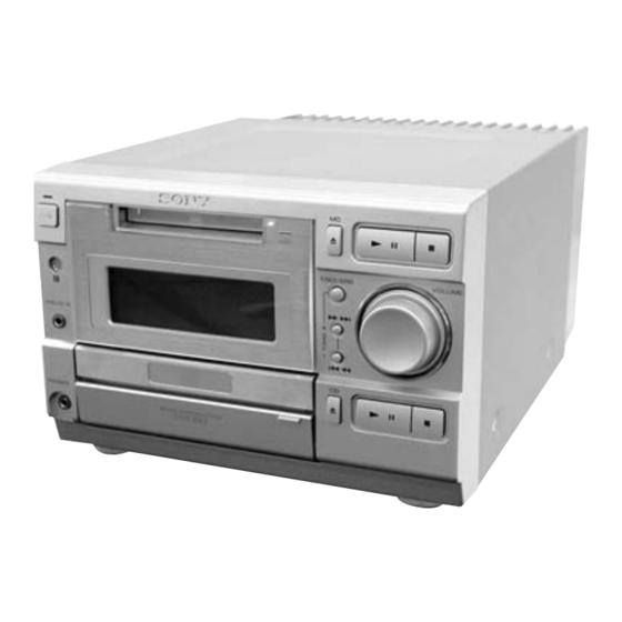
Page 19: General
SECTION 2 GENERAL LOCATION OF CONTROLS • Front View 12 3 1 I/1 button and indicator 2 Remote sensor 3 MD disc slot 4 MD Z button 5 N X (MD) button and indicator 6 x (MD) button 7 CD disc tray 8 CD Z button 9 N X (CD) button and indicator 0 x (CD) button... - Page 20 • Rear View 1 PC LINK jack 2 TAPE IN/OUT jacks 3 SPEAKER IMPEDANCE USE 6-16 Ω terminals 4 Cooling fan 5 AM ANTENNA terminals 6 TAPE CONTROL jack 7 DIGITAL OPTICAL IN jack 8 FM 75 Ω jack 9 Power cord •...
- Page 21 This section is extracted from instruction manual.
-
Page 23: Disassembly
SECTION 3 DISASSEMBLY • This set can be disassembled in the order shown below. CASE (Page 24) FRONT PANEL SECTION D.C. FAN (M901), BACK PANEL ASS’Y (Page 24) (Page 25) SP BOARD, MAIN BOARD AND RDS IC BOARD (AEP, UK models) (Page 25) MD MECHANISM DECK (MDM-7X2A) CD MECHANISM DECK (CDM55A-21BD53) - Page 24 Note: Follow the disassembly procedure in the numerical order given. CASE 4 case 1 two screws (CASE3 TP2) 1 two screws (CASE3 TP2) FRONT PANEL SECTION 1 ground wire 6 front panel section 5 wire (flat type) (29 core) (CN100) 3 three claws 2 three screws (BVTT3 ×...
- Page 25 D.C. FAN (M901), BACK PANEL ASS’Y 2 three screws 7 back panel ass’y (BVTP3 × 10) 6 D.C. fan (M901) 2 five screws (BVTP3 × 10) 5 two floating screws (PTPWH M2.6) 3 two claws 1 connector (CN109) SP BOARD, MAIN BOARD AND RDS IC BOARD (AEP, UK models) 1 two connectors (CN103, 801) 2 SP board...
- Page 26 MD MECHANISM DECK (MDM-7X2A) 4 four step screws 7 mechanism deck (BVTPWH M3) (MDM-7X2A) 1 wire (flat type) (17 core) (CN103) 1 wire (flat type) (27 core) (CN102) 6 two insulators 3 ground wire 6 insulator 2 BTN screw (1.7 × 3) 6 insulator BD (MD) BOARD 1 Remove the solder (four portions).
- Page 27 HOLDER ASS’Y 1 claw 2 holder ass’y GUIDE (L), SLIDER (EJ), SLIDER, LEVER (HEAD) 4 slider (EJ) 3 slider 2 guide (L) 1 two screws (BTP2 × 6) 6 lever (head) 5 lever (CHG)
- Page 28 OPTICAL PICK-UP (KMS-262A/J1N), OVER WRITE HEAD (HR901) 9 optical pick-up (KMS-262A/J1N) over write head (HR901) 8 main shaft 7 screw (KTP2 × 6) 7 screw (KTP2 × 6) 5 screw (BTP2 × 6) 3 screw (BTP2 × 6) 6 base (BU-A) 4 base (BU-D) 2 gear (SD) 1 screw...
- Page 29 CD MECHANISM DECK (CDM55A-21BD53) 8 base (MDM) section 5 two screws (BVTT3 × 6) 7 wire (flat type) (21 core) (CN1002) 5 two screws 2 loading panel (BVTT3 × 6) 9 screw (BVTT3 × 6) 1 two claws 4 wire (flat type) (31 core) qs CD mechanism deck (CN107)
- Page 30 BASE UNIT (BU-21BD53), HOLDER (55-BU21) 1 three floating screws (DIA. 12) 2 floating screw (PTPWH M2.6) 5 base unit (BU-21BD53) 4 two insulators 4 two insulators (BU21) (BU21) 6 two cone coil springs 6 two cone coil springs 8 holder (55-BU21) 7 shaft (BU21) TRAY (CDM), LOADING BOARD...
- Page 31 CAM (CDM55) 3 spacer (55) 4 pulley (LDG) 6 gear (B) 5 gear (A) 1 torsion spring 7 roller 8 cam (CDM55) 2 lever (SW)
-
Page 32: Test Mode
SECTION 4 TEST MODE MD SECITON Note 1: About “R” As this unit has only a few buttons, some operations require the use of remote commander (RM-S5EN/provided with unit: 1-476-086-21) buttons. These operations are indicated as “R” in this manual. [MENU/NO] Example: ...Press the... - Page 33 5. SELECTING THE TEST MODE There are 26 types of test modes as shown below. The groups can be switched by pressing the button. After “R” M > “R” selecting the group to be used, press the ENTER/YES “R” button. After setting a certain group, pressing the M >...
- Page 34 5-1. Operating the Continuous Playback Mode 1. Entering the continuous playback mode (1) Set the disc in the unit. (Whichever recordable discs or discs for playback only are available) (2) Press the . m “R” M > “R” button to display “CPLAY2MODE” (C36). (3) Press the button to change the display to “CPLAY2MID”.
- Page 35 7. TEST MODE DISPLAYS [CD-MD SYNC HIGH] Each time the button is pressed, the display changes in the following order. When CPLAY or CREC are started, the display will forcibly be switched to the error rate display as the initial mode. 1.
- Page 36 8. AUTOMATIC SELF-DIAGNOSIS FUNCTION This test mode performs CREC and CPLAY automatically for mainly checking the characteristics of the optical pick-up. To perform this test mode, the laser power must first be checked. Perform AUTO CHECK after the laser power check and Iop Compare. Procedure: 1.
-
Page 37: Electrical Adjustments
SECTION 5 ELECTRICAL ADJUSTMENTS MD SECTION Note 1:About “R” As this unit has only a few buttons, some operations require the use of remote commander (RM-S5EN/provided with unit: 1-476-086-21) buttons. These operations are indicated as “R” in this manual. [MENU/NO] Example: ...Press the button of the remote commander. - Page 38 Adjustment flow • Abbreviation Start OP: optical pick-up After turning off and then on the power, initialize the EEPROM Replace IC195 For details, refer to “WHEN MEMORY NG IS DIS- PLAYED” in 1. SERVICING NOTES (See page 12) 7. INITIAL SETTING OF ADJUSTMENT VALUE Replace OP or IC195 (See page 43) 9.
- Page 39 2. PRECAUTIONS FOR CHECKING LASER DIODE • Oscilloscope (Measure after performing CAL of prove.) • Digital voltmeter EMISSION • Thermometer To check the emission of the laser diode during adjustments, never • Jig for checking BD (MD) board waveform view directly from the top as this may lose your eye-sight. (Part No.
- Page 40 5. USING THE CONTINUOUSLY RECORDED DISC Procedure: 1. Set the laser power meter on the objective lens of the optical * This disc is used in focus bias adjustment and error rate check. pick-up. (When it cannot be set properly, press the m “R”...
- Page 41 6-4. Auto Check 6-6. Traverse Check This test mode performs CREC and CPLAY automatically for mainly checking the characteristics of the optical pick-up. To Note 1: Data will be erased during MO reading if a recorded disc is used in this adjustment. perform this test mode, the laser power must first be checked.
- Page 42 9. Press the button to display “EFB = 6-7. Focus Bias Check ENTER/YES “R” P”. Change the focus bias and check the focus tolerance amount. Then, the optical pick-up moves to the pit area automatically Procedure: and servo is imposed. 1.
- Page 43 7. INITIAL SETTING OF ADJUSTMENT VALUE 9. TEMPERATURE COMPENSATION OFFSET ADJUSTMENT Note: Save the temperature data at that time in the non-volatile memory Mode which sets the adjustment results recorded in the non-volatile as 25 ˚C reference data. memory to the initial setting value. However the results of the tempera- Note: ture compensation offset adjustment will not change to the initial setting 1.
- Page 44 6. Press the . m “R” M > “R” button so that the button. YES “R” reading of the laser power meter becomes 6.9 to 7.1 mW, press 4. After “Complete!” is displayed momentarily, the display changes ENTER/YES “R” button to save it. to “Iop 7.0 mW”.
- Page 45 8. Press the . m “R” M > “R” button so that the 18. Press the button, display “EFB = SAVE” ENTER/YES “R” waveform of the oscilloscope becomes the specified value. for a moment and save the adjustment results in the non-volatile (When the .
- Page 46 14. ERROR RATE CHECK 16. AUTO GAIN CONTROL OUTPUT LEVEL ADJUSTMENT 14-1. CD Error Rate Check Be sure to perform this adjustment when the optical pick-up is Procedure: replaced. 1. Load the check disc (TDYS-1). If the adjustment results becomes “Adjust NG!”, the optical pick- 2.
- Page 47 Adjustment and checking Loacation: – BD (MD) BOARD (Component Side) – – BD (MD) BOARD (Conductor Side) – D101 IC101 CN105 1. I+3V CN101 2. IOP 3. GND 4. TE 5. FE 6. VC 7. RF IC151 IC190 Note: It is useful to use the jig for checking the waveform. (Refer to Ser- vicing Notes on page 11)
-
Page 48: Cd Section
Note: A clear RF signal waveform means that the shape “◊” can be clearly CD SECTION distinguished at the center of the waveform. Note: RF signal waveform 1. CD Block is basically designed to operate without adjustment. There- VOLT/DIV: 200 mV fore, check each item in order given. - Page 49 Checking Location: – BD (CD) BOARD (Conductor Side) – (VC) IC171 (FE) TP (TE) TP (RF) IC101...
- Page 50 MEMO...
-
Page 51: Diagrams
HCD-MD595 SECTION 6 DIAGRAMS 6-1. BLOCK DIAGRAM – MD SERVO Section – DIGITAL SIGNAL PROCESSOR, EFM/ACIRC ENCODER/DECODER, SHOCK PROOF MEMORY CONTROLLER, ATRAC ENCODER/DECODER OVER WRITE IC151 (1/2) EFMO ADDT DADTI HEAD DRIVE (Page 52) IC181, Q181, 182 DATAI SAMPLING HR901... -
Page 52: Block Diagram - D/A, A/D Converter Section
HCD-MD595 6-2. BLOCK DIAGRAMS – D/A, A/D CONVERTER Section – VINL (Page 53) DADTI DAT AO DIGITAL DECIMATION (Page 51) CANCELLATION CONVERTER INTERFACE FILTER VINR FILTER BLOCK R-CH A/D CONVERTER SCLK CLOCK CONTROL IC1005 • R-ch is omitted due to same as L-ch. -
Page 53: Block Diagram - Main Section
HCD-MD595 6-3. BLOCK DIAGRAM – MAIN Section – (Page 52) J101 (2/2) TAPE OUT R-CH MUTING Q101 R-CH J602 R-CH MUTING ANALOG CONTROL Q102 J601 R-CH PHONES INPUT SELECT SWITCH, J101 (1/2) TONE CONTROL, ELECTRICAL VOLUME IC301 TAPE IN R-CH... -
Page 54: Block Diagram - Display, Power Supply Section
HCD-MD595 6-4. BLOCK DIAGRAM – DISPLAY, POWER SUPPLY Section – LIQUID CRYSTAL DISPLAY UNIT • Abbreviation LCD600 : Australian model LCD DATA : Canadian model LCD CLK : Hong Kong model RW/CS LCD CE : Tourist model LCD CLEAR : Malaysia model : Singapore model D607 –... -
Page 55: Note For Printed Wiring Boards And Schematic Diagrams
6-5. NOTE FOR PRINTED WIRING BOARDS AND SCHEMATIC DIAGRAMS • Circuit Boards Location (In addition to this, the necessary note is printed in each block) Note on Schematic Diagram: Note on Printed Wiring Boards: AMP board • X : parts extracted from the component side. •... -
Page 56: Printed Wiring Board - Bd (Cd) Board
HCD-MD595 6-6. PRINTED WIRING BOARD – BD (CD) Board – • See page 55 for Circuit Boards Location. MD DIGITAL BOARD CN1002 (Page 65) There are a few cases that the part isn't mounted in model is printed on diagrams. -
Page 57: Schematic Diagram - Bd (Cd) Board
HCD-MD595 6-7. SCHEMATIC DIAGRAM – BD (CD) Board – • See page 76 for waveforms. (Page • Voltages and waveforms are dc with respect to ground The components identified by mark 0 or dotted Les composants identifiés par une marque 0 sont under no-signal conditions. -
Page 58: Schematic Diagram - Bd (Md) Board (1/2)
HCD-MD595 6-8. SCHEMATIC DIAGRAM – BD (MD) Board (1/2) – • • See page 76 for waveforms. See page 77 for IC Block Diagram. (Page 59) (Page 59) (Page 59) • Voltages and waveforms are dc with respect to ground The components identified by mark 0 or dotted Les composants identifiés par une marque 0 sont... -
Page 59: Schematic Diagram - Bd (Md) Board (2/2)
HCD-MD595 6-9. SCHEMATIC DIAGRAM – BD (MD) Board (2/2) – • • See page 76 for waveforms. See page 77 for IC Block Diagram. (Page 58) (Page 61) (Page 58) (Page 63) (Page 58) • Voltages and waveforms are dc with respect to ground under no-signal conditions. -
Page 60: Printed Wiring Board - Bd (Md) Board
HCD-MD595 6-10. PRINTED WIRING BOARD – BD (MD) Board – • See page 55 for Circuit Boards Location. BD (MD) BOARD FLEXIBLE BOARD BD (MD) BOARD (CONDUCTOR SIDE) (COMPONENT SIDE) 1-678-514- S102-2 PROTECT (LOADING) –1 DETECT –2 S102-1 REFLECT RATE... -
Page 61: Schematic Diagram - Md Digital Board (1/3)
HCD-MD595 6-11. SCHEMATIC DIAGRAM – MD DIGITAL Board (1/3) – • • See page 76 for waveform. See page 77 for IC Block Diagram. (Page (Page 62) (Page 63) • Voltages and waveforms are dc with respect to ground under no-signal conditions. -
Page 62: Schematic Diagram - Md Digital Board (2/3)
HCD-MD595 6-12. SCHEMATIC DIAGRAM – MD DIGITAL Board (2/3) – • • See page 76 for waveform. See page 77 for IC Block Diagram. (Page 61) (Page 57) (Page 63) • Voltages and waveforms are dc with respect to ground under no-signal conditions. -
Page 63: Schematic Diagram - Md Digital Board (3/3)
HCD-MD595 6-13. SCHEMATIC DIAGRAM – MD DIGITAL Board (3/3) – • • See page 76 for waveforms. See page 77 for IC Block Diagrams. (Page 62) (Page 66) (Page • Voltages and waveforms are dc with respect to ground (Page 61) under no-signal conditions. -
Page 64: Printed Wiring Board - Md Digital Board (Component Side)
HCD-MD595 6-14. PRINTED WIRING BOARD – MD DIGITAL Board (Component Side) – • See page 55 for Circuit Boards Location. • Semiconductor Location Ref. No. Location D1104 D1106 IC1001 IC1002 IC1005 IC1006 IC1008 IC1101 Q1003 Q1004 Q1103... -
Page 65: Printed Wiring Boards - Md Digital (Conductor Side)/Loading Boards
HCD-MD595 6-15. PRINTED WIRING BOARDS – MD DIGITAL (Conductor Side)/LOADING Boards – • See page 55 for Circuit Boards Location. MD DIGITAL BOARD CN1005 CLOSE OPEN M201 CD TRAY OPEN/CLOSE (Page 60) DETECT (Page 60) • Semiconductor Location Ref. No. -
Page 66: Schematic Diagram - Main (1/2)/Rds Ic Boards
HCD-MD595 6-16. SCHEMATIC DIAGRAM – MAIN (1/2)/RDS IC Boards – • See page 77 for IC Block Diagrams. (Page 63) (Page 69) (Page 67) (Page 67) (Page 75) • Voltages and waveforms are dc with respect to ground under no-signal (detuned) conditions. -
Page 67: Schematic Diagram - Main Board (2/2)
HCD-MD595 6-17. SCHEMATIC DIAGRAM – MAIN Board (2/2) – • See page 76 for waveforms. (Page 73) (Page 66) (Page 66) • Voltages and waveforms are dc with respect to ground under no-signal (detuned) conditions. no mark : FM... -
Page 68: Printed Wiring Boards - Main/Rds Ic Boards
HCD-MD595 6-18. PRINTED WIRING BOARDS – MAIN/RDS IC Boards – • See page 55 for Circuit Boards Location. (Page 65) (Page 69) (Page 72) (Page 74) • Semiconductor Location Ref. No. Location Ref. No. Location Ref. No. Location Ref. No. -
Page 69: Printed Wiring Board - Sp Board
HCD-MD595 6-19. PRINTED WIRING BOARD – SP Board – • 6-20. SCHEMATIC DIAGRAM – SP Board – See page 55 for Circuit Boards Location. (Page 68) (Page 71) (Page 66) • Voltages and waveforms are dc with respect to ground under no-signal (detuned) conditions. -
Page 70: Printed Wiring Board - Amp Board
HCD-MD595 6-21. PRINTED WIRING BOARD – AMP Board – • See page 55 for Circuit Boards Location. (Page 74) (Page 69) • Semiconductor Location Ref. No. Location D801 D802 D832 D851 D852 IC801 Q801 Q802 Q841 Q851 Q852 Q871 Q872... -
Page 71: Schematic Diagram - Amp Board
HCD-MD595 6-22. SCHEMATIC DIAGRAM – AMP Board – (Page 69) (Page 75) • Voltages and waveforms are dc with respect to ground under no-signal (detuned) conditions. no mark : FM The components identified by mark 0 or dotted Les composants identifiés par une marque 0 sont line with mark 0 are critical for safety. -
Page 72: Printed Wiring Boards - Panel/Bl Boards
HCD-MD595 6-23. PRINTED WIRING BOARDS – PANEL/BL Boards – • See page 55 for Circuit Boards Location. • Semiconductor Location Ref. No. Location D601 D602 D603 D604 D605 D606 IC602 Q601 Q602 Q603 Q604 Q605 Q606 Q608 Q609 Q610 (Page 68) There are a few cases that the part isn't mounted in model is printed on diagrams. -
Page 73: Schematic Diagram - Panel/Bl Boards
HCD-MD595 6-24. SCHEMATIC DIAGRAM – PANEL/BL Boards – (Page 67) • Voltages and waveforms are dc with respect to ground under no-signal (detuned) conditions. no mark : FM... -
Page 74: Printed Wiring Board - Power Board
HCD-MD595 6-25. PRINTED WIRING BOARD – POWER Board – • See page 55 for Circuit Boards Location. • Semiconductor (Page 70) Location Ref. No. Location D921 D971 D972 D973 D974 D981 D982 D983 D984 D985 D991 D992 D993 IC921 Q991... -
Page 75: Schematic Diagram - Power Board
HCD-MD595 6-26. SCHEMATIC DIAGRAM – POWER Board – (Page 71) (Page 66) • Voltages and waveforms are dc with respect to ground under no-signal (detuned) conditions. no mark : FM The components identified by mark 0 or dotted Les composants identifiés par une marque 0 sont line with mark 0 are critical for safety. - Page 76 • Waveforms – BD (MD) Board – – MD DIGITAL Board – – MAIN Board – – BD (CD) Board – 1 IC101 wg (MDP) (CD PLAY mode) 6 IC101 us (XTAO) 1 IC101 1 (I), 2 (J) (MD PLAY mode) 1 IC1101 el (X1) 1 IC501 eg (XTIN) 2.6 Vp-p...
- Page 77 • IC Block Diagrams – BD (MD) Board – IC101 CXA2523AR 43 42 USROP – RF AGC – USRC RFA1 BPF3T RFA2 RFA3 PEAK3T – HLPT –1 – – –2 – OFST PTGR TEMP PEAK – –2 – BOTTOM 36 BOTM –...
- Page 78 IC141 BH6511FS INTERFACE INTERFACE CHARGE PREDRIVE PREDRIVE PUMP. PREDRIVE PREDRIVE INTERFACE INTERFACE IC151 CXD2662R 100 99 98 97 96 95 94 93 92 91 90 89 88 87 86 85 84 83 82 81 80 79 78 77 76 SPINDLE GENERATOR SERVO 75 TE...
- Page 79 – MD DIGITAL Board – IC1005 µDA1360TS IC1004 LB1641 VDDA T.S.D O.C.P VSSA MOTOR MOTOR 14 FSEL DRIVE DRIVE VINL CLOCK – CONTROL VREF CANCELLATION DECIMATION FILTER FILTER FWD/REV/STOP 13 DATAO DIGITAL CONTROL LOGIC VINR – 12 WS INTERFACE 11 BCK VREF (N) VREF (P) 10 VSSD...
- Page 80 IC301 M62428AFP6000C AVDD VREF REF AMP AGND – VREFI VREFO SUR R SURROUND SW MIC IN AGND SUR C IN1A IN2A IN1B – IN2B IN1C BUFF BUFF AMP1 AMP2 IN2C IN1D IN2D AMP1 AMP2 REC OUT1 REC OUT2 INBAS1 INBAS2 BASS BASS AMP1...
-
Page 81: Ic Pin Function Description
6-27. IC PIN FUNCTION DESCRIPTION • BD (MD) BOARD IC101 CXA2523AR (RF AMP, FOCUS/TRACKING ERROR AMP) Pin No. Pin Name Description I-V converted RF signal I input from the optical pick-up block detector I-V converted RF signal J input from the optical pick-up block detector Middle point voltage (+1.65V) generation output terminal 4 to 9 A to F... - Page 82 • BD (MD) BOARD IC151 CXD2662R (DIGITAL SIGNAL PROCESSOR, DIGITAL SERVO PROCESSOR, EFM/ACIRC ENCODER/DECODER, SHOCK PROOF MEMORY CONTROLLER, ATRAC ENCODER/DECODER) Pin No. Pin Name Description Focus OK signal output terminal “H” is output when focus is on (“L”: NG) MNT0 (FOK) Not used (open) MNT1 (SHOCK) Track jump detection signal output to the MD mechanism controller (IC1001)
- Page 83 Pin No. Pin Name Description XCAS Column address strobe signal output to the D-RAM (IC152) “L” active Address signal output to the D-RAM (IC152) XRAS Row address strobe signal output to the D-RAM (IC152) “L” active Write enable signal output to the D-RAM (IC152) “L” active Two-way data bus with the D-RAM (IC152) MVCI I (S)
- Page 84 Pin No. Pin Name Description FRDR Focus servo drive PWM signal (–) output to the BH6511FS (IC141) Clock signal (176.4 kHz) output terminal (X’tal system) Not used (open) SRDR Sled servo drive PWM signal (–) output to the BH6511FS (IC141) SFDR Sled servo drive PWM signal (+) output to the BH6511FS (IC141) SPRD...
- Page 85 • MD DIGITAL BOARD IC1001 M30805SGP (MD MECHANISM CONTROLLER) Pin No. Pin Name Description 1, 2 — Not used (open) LVL1 L-ch level output terminal Not used (open) LVL0 R-ch level output terminal Not used (open) 5 to 7 — Not used (open) MUTE Muting control signal output to the D/A converter (IC1006) “L”: muting...
- Page 86 Pin No. Pin Name Description C2-PWM-B Not used (open) XINT Interrupt status input from the CXD2662R (IC151) — Not used (open) XELT Not used (open) Laser power select signal output to the CXD2662R (IC151) and HF module switch circuit WR-PWR “L”: playback mode, “H”: recording mode I2CCLK Shift clock signal input/output terminal for the IIC bus...
- Page 87 Pin No. Pin Name Description VCC3 — Power supply terminal (+3.3V) Address signal output to the flash memory (IC1002) VSS3 — Ground terminal 77 to 85 A17 to A9 Address signal output to the flash memory (IC1002) 86 to 89 SEL3 to SEL0 Model destination setting input terminal Writing protect signal output to the flash memory (IC1002)
- Page 88 • MD DIGITAL BOARD IC1101 µPDSS3033AYGF-M05-3BA (CD MECHANISM CONTROLLER) Pin No. Pin Name Description DRVDAT Serial data output to a FL driver Not used (open) DRVCLK Serial data transfer clock signal output to a FL driver Not used I2CDAT Data input/output terminal for the IIC bus Not used (open) I2CCLK Shift clock signal input/output terminal for the IIC bus...
- Page 89 Pin No. Pin Name Description IN-SW Detection input from the tray open/close detect switch (S1) “L”: when tray is close CD loading motor (M201) control signal output to the motor driver IC (IC1102) LOD POS “L” active *1 CD loading motor (M201) control signal output to the motor driver IC (IC1102) LOD NEG “L”...
- Page 90 • MAIN BOARD IC501 µPDSS3033AYGF-M11-3BA (SYSTEM CONTROLLER) Pin No. Pin Name Description GEQ DATA Serial data output to the M62428AFP (IC301) GEQ CLK Serial data transfer clock signal output to the M62428AFP (IC301) IIC DAT Data input/output terminal for the IIC bus CANT USE Not used (fixed at “L”) IIC CLK...
- Page 91 Pin No. Pin Name Description Power down detection signal output to the MD mechanism controller (IC1001) and CD MD/CD POWER mechanism controller (IC1101) TR RELAY Standby relay (RY991) control signal output “L”: speaker off RECMUTE Muting on/off control signal output of tape output signal “L”: muting on DIMMER LCD back light on/off control signal output “H”: LED on GC POWER...
- Page 92 Pin No. Pin Name Description PC POWER Power on request signal input from the PC LINK jack (CN104) SIRCS Remote control signal input from the remote control receiver (IC602) AC CUT IN AC power off detection signal input terminal Not used (open) RDS DATA RDS serial data input from the RDS decoder (IC401) Used for the AEP, UK models RDS serial data transfer clock signal input from the RDS decoder (IC401)
-
Page 93: Exploded Views
SECTION 7 Ver. 1.1 EXPLODED VIEWS NOTE: • -XX and -X mean standardized parts, so they • Items marked “*” are not stocked since they The components identified by mark 0 or dotted line with mark may have some difference from the original are seldom required for routine service. - Page 94 (2) CHASSIS SECTION MDM-7X2A not supplied not supplied M901 not supplied supplied T900 not supplied supplied not supplied CDM55A-21BD53...
- Page 95 Ref. No. Part No. Description Remark Ref. No. Part No. Description Remark 1-792-831-11 WIRE (FLAT TYPE) (21 CORE) X-4953-287-1 PANEL ASSY, BACK (MY, SP, HK, JE) 1-773-315-11 WIRE (FLAT TYPE) (31 CORE) X-4953-289-1 PANEL ASSY, BACK (AUS) A-4473-547-A MD DIGITAL BOARD, COMPLETE 4-228-095-11 PANEL, BACK (AEP, UK) 4-228-097-01 BASE (MDM) 4-228-095-21 PANEL, BACK (US, CND)
- Page 96 Ver. 1.1 (3) MD MECHANISM DECK SECTION-1 (MDM-7X2A) Ref. No. Part No. Description Remark Ref. No. Part No. Description Remark * 301 4-996-267-01 BASE (BU-D) 4-227-012-01 SPRING (HOLDER), TENSION 4-908-618-21 SCREW (+BTP) (2X6) 4-227-019-02 PLATE (HOLDER), RETAINER 4-227-007-01 GEAR (SB) 4-227-013-01 SPRING (EJ), TENSION 4-227-025-01 BELT (LOADING) 4-226-996-01 LIMITTER (EJ)
- Page 97 (4) MD MECHANISM DECK SECTION-2 (MDM-7X2A) HR901 S102 M101 M102 The components identified by mark 0 or dotted line with mark 0 are critical for safety. Replace only with part number M103 specified. Les composants identifiés par une marque 0 sont critiquens pour la sécurité.
- Page 98 (5) CD MECHANISM DECK SECTION (CDM55A-21BD53) M201 The components identified by mark 0 or dotted line with mark 0 are critical for safety. Replace only with part number specified. Les composants identifiés par une marque 0 sont critiquens pour la sécurité.
-
Page 99: Electrical Parts List
SECTION 8 ELECTRICAL PARTS LIST NOTE: • Due to standardization, replacements in the • Items marked “*” are not stocked since they The components identified by mark 0 or dotted line with mark are seldom required for routine service. parts list may be different from the parts speci- 0 are critical for safety. - Page 100 BD (MD) Ref. No. Part No. Description Remark Ref. No. Part No. Description Remark 0 R831 1-212-881-11 FUSIBLE 1/4W F R841 1-249-437-11 CARBON 1/4W C145 1-164-156-11 CERAMIC CHIP 0.1uF R842 1-249-437-11 CARBON 1/4W C146 1-117-720-11 CERAMIC CHIP 4.7uF C147 1-117-720-11 CERAMIC CHIP 4.7uF R843 1-249-441-11 CARBON...
- Page 101 BD (MD) Ref. No. Part No. Description Remark Ref. No. Part No. Description Remark IC195 8-759-640-41 IC BR24C08F-E2 R114 1-216-827-11 METAL CHIP 3.3K 1/16W R115 1-216-833-11 METAL CHIP 1/16W < SHORT > R116 1-216-839-11 METAL CHIP 1/16W JW201 1-216-295-11 SHORT R117 1-216-837-11 METAL CHIP 1/16W...
- Page 102 BD (MD) LOADING MAIN Ref. No. Part No. Description Remark Ref. No. Part No. Description Remark < VIBRATOR > C142 1-126-933-11 ELECT 100uF X171 1-781-569-21 OSCILLATOR, CRYSTAL (90.3168MHz) C144 1-126-925-11 ELECT 470uF C145 1-126-933-11 ELECT 100uF ************************************************************** C146 1-124-698-81 ELECT 100uF 1-678-380-11 BL BOARD C151...
- Page 103 MAIN Ref. No. Part No. Description Remark Ref. No. Part No. Description Remark < COIL > C902 1-126-767-11 ELECT 1000uF C905 1-126-926-11 ELECT 1000uF FB111 1-412-473-21 INDUCTOR C906 1-126-964-11 ELECT 10uF FB112 1-412-473-21 INDUCTOR C907 1-126-925-11 ELECT 470uF C911 1-126-925-11 ELECT 470uF <...
- Page 104 MAIN Ref. No. Part No. Description Remark Ref. No. Part No. Description Remark R152 1-249-417-11 CARBON 1/4W R511 1-249-429-11 CARBON 1/4W R153 1-249-429-11 CARBON 1/4W R512 1-249-417-11 CARBON 1/4W R154 1-249-417-11 CARBON 1/4W R513 1-247-807-31 CARBON 1/4W R155 1-249-441-11 CARBON 100K 1/4W R514...
- Page 105 MAIN MD DIGITAL Ref. No. Part No. Description Remark Ref. No. Part No. Description Remark < VIBRATOR > C1106 1-163-038-11 CERAMIC CHIP 0.1uF X501 1-781-107-21 VIBRATOR, CERAMIC (16MHz) C1107 1-126-960-11 ELECT X502 1-567-098-41 VIBRATOR, CRYSTAL (32.768kHz) C1108 1-163-038-11 CERAMIC CHIP 0.1uF C1109 1-163-038-11 CERAMIC CHIP...
- Page 106 MD DIGITAL PANEL Ref. No. Part No. Description Remark Ref. No. Part No. Description Remark R1002 1-216-066-00 METAL CHIP 5.1K 1/10W R1093 1-216-033-00 METAL CHIP 1/10W R1005 1-216-025-11 RES-CHIP 1/10W R1006 1-216-025-11 RES-CHIP 1/10W R1094 1-216-033-00 METAL CHIP 1/10W R1007 1-216-025-11 RES-CHIP 1/10W R1095...
- Page 107 PANEL POWER Ref. No. Part No. Description Remark Ref. No. Part No. Description Remark C619 1-162-282-31 CERAMIC 100PF R622 1-249-425-11 CARBON 4.7K 1/4W R623 1-249-425-11 CARBON 4.7K 1/4W C620 1-162-286-31 CERAMIC 220PF R625 1-249-402-11 CARBON 1/4W C621 1-162-286-31 CERAMIC 220PF R631 1-249-413-11 CARBON 1/4W...
- Page 108 POWER RDS IC Ref. No. Part No. Description Remark Ref. No. Part No. Description Remark C982 1-115-364-11 ELECT 22000uF < TRANSFORMER > C983 1-136-165-00 FILM 0.1uF 0 T901 C984 1-128-548-11 ELECT 4700uF 1-435-573-11 TRANSFORMER, POWER (AEP, UK) 0 C991 0 T901 1-113-925-11 CERAMIC 0.01uF 250V...
- Page 109 Ref. No. Part No. Description Remark Ref. No. Part No. Description Remark Q881 8-729-620-05 TRANSISTOR 2SC2603-EF M102 A-4672-900-A MOTOR ASSY, SLED (for MD) < RESISTOR > M103 A-4672-975-A MOTOR ASSY, LOADING (for MD) M201 A-4672-771-A MOTOR (LD) ASSY (LOADING) (for CD) R875 1-249-441-11 CARBON 100K...
- Page 110 HCD-MD595 REVISION HISTORY Clicking the version allows you to jump to the revised page. Also, clicking the version at the upper right on the revised page allows you to jump to the next revised page. Ver. Date Description of Revision 2000.08...