Table of Contents
Advertisement
Quick Links
TABLE OF CONTENTS
1 Safety Precautions----------------------------------------------- 3
1.1. General Guidelines---------------------------------------- 3
1.2. Caution for AC Cord (For GS only) ------------------- 4
1.3. Before Use (For PH only)-------------------------------- 4
1.4. Before Repair and Adjustment ------------------------- 4
1.5. Protection Circuitry ---------------------------------------- 5
Model No.
Product Color: (K)...Black Type
PAGE
1.6. Safety Part Information -----------------------------------5
2 Warning --------------------------------------------------------------6
to Electrostatically Sensitive (ES) Devices ----------6
3 Service Navigation -----------------------------------------------8
© Panasonic Corporation 2014. All rights reserved.
Unauthorized copying and distribution is a violation of
law.
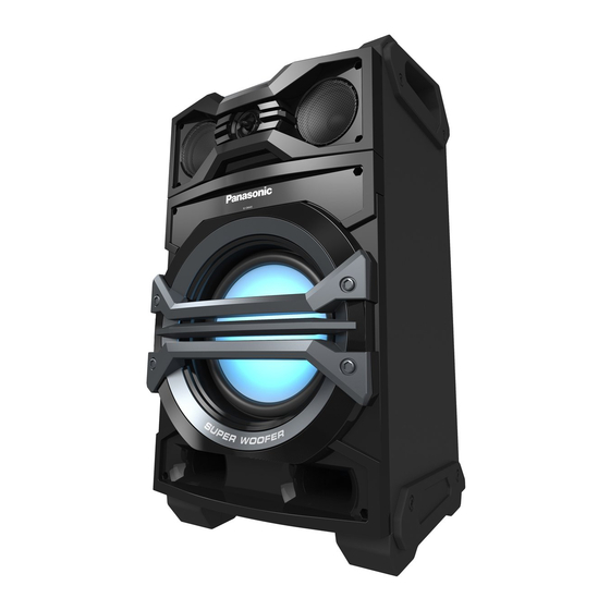
Active Speaker System
SC-CMAX5GS
SC-CMAX5PH
SC-CMAX5PR
PSG1408001CE
PAGE
Advertisement
Table of Contents

Related Manuals for Panasonic SC-CMAX5GS


Summary of Contents for Panasonic SC-CMAX5GS
-
Page 1: Table Of Contents
1.4. Before Repair and Adjustment ------------------------- 4 2.2. Service caution based on Legal restrictions --------7 1.5. Protection Circuitry ---------------------------------------- 5 3 Service Navigation -----------------------------------------------8 © Panasonic Corporation 2014. All rights reserved. Unauthorized copying and distribution is a violation of law. - Page 2 3.1. Service Information ----------------------------------------8 12.12. PANEL CIRCUIT (3/3)---------------------------------- 63 4 Specifications ------------------------------------------------------9 12.13. FL DISPLAY CIRCUIT---------------------------------- 64 5 Location of Controls and Components------------------ 10 13 Printed Circuit Board------------------------------------------ 65 5.1. Main Unit & Remote Control Key Button 13.1. MAIN P.C.B. ASS’Y (Side A)-------------------------- 65 Operations (For PH/PR) -------------------------------- 10 13.2.
-
Page 3: Safety Precautions
1 Safety Precautions 1.1. General Guidelines 1. IMPORTANT SAFETY NOTICE There are special components used in this equipment which are important for safety. These parts are marked by in the Schematic Diagrams, Circuit Board Layout, Exploded Views and Replacement Parts List. It is essential that these critical parts should be replaced with manufacturer’s specified parts to prevent X-RADIATION, shock, fire, or other hazards. -
Page 4: Caution For Ac Cord (For Gs Only)
1.2. Caution for AC Cord (For GS only) Figure 1-2 1.3. Before Use (For PH only) Be sure to disconnect the AC cord before adjusting the voltage selector. Use a minus(-) screwdriver to set the voltage selector (on the bottom panel) to the voltage setting for the area in which the unit will be used. -
Page 5: Protection Circuitry
1.5. Protection Circuitry The protection circuitry may have operated if either of the following conditions are noticed: • No sound is heard when the power is turned on. • Sound stops during a performance. The function of this circuitry is to prevent circuitry damage if, for example, the positive and negative speaker connection wires are "shorted", or if speaker systems with an impedance less than the indicated rated impedance of the amplifier are used. -
Page 6: Warning
2 Warning 2.1. Prevention of Electrostatic Discharge (ESD) to Electrostatically Sensi- tive (ES) Devices Some semiconductor (solid state) devices can be damaged easily by static electricity. Such components commonly are called Elec- trostatically Sensitive (ES) Devices. The following techniques should be used to help reduce the incidence of component damage caused by electrostatic discharge (ESD). -
Page 7: Service Caution Based On Legal Restrictions
2.2. Service caution based on Legal restrictions 2.2.1. General description about Lead Free Solder (PbF) The lead free solder has been used in the mounting process of all electrical components on the printed circuit boards used for this equipment in considering the globally environmental conservation. The normal solder is the alloy of tin (Sn) and lead (Pb). -
Page 8: Service Navigation
3 Service Navigation 3.1. Service Information This service manual contains technical information which will allow service personnel’s to understand and service this model. Please place orders using the parts list and not the drawing reference numbers. If the circuit is changed or modified, this information will be followed by supplement service manual to be filed with original service manual. -
Page 9: Specifications
4 Specifications • Specifications are subject to change without notice. • Mass and dimensions are approximate. • Total harmonic distortion is measured by the digital spectrum ana- lyzer. General Power consumption 92 W *Trolley handle at fully pushed-down position Power consumption in standby Approx. -
Page 10: Location Of Controls And Components
5 Location of Controls and Components 5.1. Main Unit & Remote Control Key Button Operations (For PH/PR) -
Page 11: Main Unit & Remote Control Key Button Operations (For Gs)
5.2. Main Unit & Remote Control Key Button Operations (For GS) -
Page 12: Service Mode
6 Service Mode This unit is equipped with features of service mode & doctor mode setting for checking the functions & reliability. 6.1. Self Diagnostic Mode Step 1 : Select USB A mode Step 1 : In service mode Press [SETUP] on the remote control. -
Page 13: Self Diagnostic Function Error Code
6.2. Self Diagnostic Function Error Code Self-Diagnostic Function provides information on any problems occurring for the unit and its respective components by displaying the error codes. These error code such as U**, H** and F** are stored in memory and held unless it is cleared. The error code is automatically display after entering into self-diagnostic mode. -
Page 14: Doctor Mode
6.3. Doctor Mode Note : To enter the Doctor Mode, please use MAX770 remote control. (Part No : N2QAYB000915) 6.3.1. Doctor Mode Table 1 Item Key Operation FL Display Mode Name Description Front Key Doctor Mode AUX Mode: To enter into Doctor Mode for (Display 1) 1. - Page 15 6.3.2. Doctor Mode Table 2 Item Key Operation FL Display Mode Name Description Front Key Bluetooth mac Bluetooth Address Check In Doctor Mode: Address Checking 1. Press [10] [1] and display will show. 2. To cancel this mode press Display of BlueTooth MAC Address will scroll [POWER, /I] button on forever Main Unit...
-
Page 17: Troubleshooting Guide
7 Troubleshooting Guide ● Reset Method (Factory Shipment Status) . Plug In AC cord together with (no 2) Press and hold the power button for 4 seconds then FL display will show RESET for 2 seconds 3. Turn off the power. ●... - Page 18 IC1001 IC4803 IC4001 Mid/Hi Speaker YAMAHA C1AB00003800 SW Speaker Check Command From SoC Pin 4,5 Check IC Supply IC4001 Check Xtal Opera on (3.3V) : Pin 21,40 Troubleshoo ng X4001 (24 MHz) Check Audio Input Pin : 6 (Mic ) Digital Data Square wave Pin : 7 (AUX - Non GS/JPN) (0-3.3V )
- Page 19 Change D-AMP IC Check Spekaer Output JK3503 : Sub Woofer Ch Result : +36V (VDD) SW : IC3101 DAMP + Terminal to GND Hi/Mid : IC3301 JK3502 : Mid/Hi Ch Troubleshoo ng - Terminal to GND Check D-AMP IC Result : +18V (1/2 SW : IC3301 VDD) Hi/Mid : IC3301...
-
Page 21: Disassembly And Assembly Instructions
8 Disassembly and Assembly Instructions • This section describes the disassembly and/or assembly procedures for all major printed circuit boards & main compo- nents for the unit. (You may refer to the section of “Main components and P.C.B Locations” as described in the service manual) •... -
Page 22: Disassembly Flow Chart
8.1. Disassembly flow chart The following chart is the procedure for disassembling the casing and inside parts for internal inspection when carrying out the ser- vicing. To assemble the unit, reverse the steps shown in the chart below. 8.1.1. Amp Unit 8.1.2. -
Page 23: Type Of Screws
8.2. Type of screws 8.3. Main Parts Location Diagram... -
Page 24: Disassembly Of Handle Bar Unit
8.4. Disassembly of Handle Bar 8.5. Disassembly of Rear Panel Unit • Refer to “Disassembly of Handle Bar Unit” Step 1 : Remove 6 screws. Step 1 : Remove 4 screws. Caution : During assembling, fixed the screws in sequence Step 2 : Remove Handle Bar Unit. - Page 25 • (For PH only) Step 5 : Detach 2P Fan wires at connector (CN2101) on the Step 4 : Remove Voltage Selector P.C.B. as shown. Main P.C.B. Assembly. Caution: During assembling, ensure Voltage Selector Step 6 : Remove Rear Panel. P.C.B.
-
Page 26: Disassembly Of Amp Unit Block
8.6. Disassembly of Amp Unit Step 8 : Place Amp Unit Block on the support block. Step 9 : Cut the cable tie. Block Step 10 : Detach 4P wire at connector (CN2604) on Main • Refer to “Disassembly of Handle Bar Unit” P.C.B. -
Page 27: Disassembly Of Main P.c.b. Assembly
8.7. Disassembly of Main P.C.B. 8.8. Disassembly of SMPS Module Assembly & Voltage Selector P.C.B. • Refer to “Disassembly of Handle Bar Unit” • Refer to “Disassembly of Handle Bar Unit” • Refer to “Disassembly of Rear Panel” • Refer to “Disassembly of Rear Panel” •... -
Page 28: Disassembly Of Top Panel Unit
8.9. Disassembly of Top Panel Unit 8.10. Disassembly of Bluetooth P.C.B. Assembly • Refer to “Disassembly of Handle Bar Unit” • Refer to “Disassembly of Rear Panel” • Refer to “Disassembly of Handle Bar Unit” • Refer to “Disassembly of Amp Unit Block” •... -
Page 29: Disassembly Of Panel P.c.b
8.11. Disassembly of Panel P.C.B. Step 3 : Remove 15 screws. • Refer to “Disassembly of Handle Bar Unit” • Refer to “Disassembly of Rear Panel” • Refer to “Disassembly of Amp Unit Block” • Refer to “Disassembly of Top Panel Unit” •... -
Page 30: Disassembly Of Fl Display P.c.b
Step 5 : Detach 30P FFC at connector (CN6005) on Panel 8.12. Disassembly of FL Display P.C.B.. P.C.B. Step 6 : Remove Panel P.C.B.. • Refer to “Disassembly of Handle Bar Unit” • Refer to “Disassembly of Rear Panel” • Refer to “Disassembly of Amp Unit Block” •... -
Page 31: Disassembly Of Top Front Panel Block
8.13. Disassembly of Top Front Step 3 : Detach speaker wire. Step 4 : Remove Top Front Panel Block. Panel Block Step 1 : Remove 4 screws. Step 2 : Detach Top Front Panel Block. -
Page 32: Disassembly Of Tweeter Speaker (6Cm)
8.14. Disassembly of Tweeter 8.15. Disassembly of Woofer Speaker (6cm) Speaker (10cm) • Refer to “Disassembly of Top Front Panel Block” • Refer to “Disassembly of Top Front Panel Block” Step 1 : Detach speaker wire. Step 1 : Detach speaker wire. Step 2 : Remove 4 screws. -
Page 33: Disassembly Of Center Front Panel
8.16. Disassembly of Center Front Caution 1 : Scrape off and clean up the remaining glue at the boss and hole. Panel Caution 2 : During assembling, align the hole of the Boss with the Center Front Panel and fix it properly. Step 1 : Remove 2 screws. -
Page 34: Disassembly Of Subwoofer Front Panel Block
8.17. Disassembly of Subwoofer Step 2 : Insert flathead screwdriver into the grooves. Step 3 : Apply light force to push the Subwoofer Front Panel Front Panel Block Block as arrow shown. • Refer to “Disassembly of Center Front Panel” Step 4 : Insert a steel rule in between the Subwoofer Front Panel Block and Speaker Cabinet Assembly. - Page 35 Step 6 : Lift up himelon. Caution 1 : Scrape off and clean up the remaining glue at the boss and hole. Caution : Replace the himelon if they are torn during disas- Caution 2 : During assembling, align the holes of the sembling.
-
Page 36: Disassembly Of Woofer Speaker (25Cm)
8.18. Disassembly of Woofer 8.19. Disassembly of Lighting Wire Speaker (25cm) P.C.B. Assembly • Refer to “Disassembly of Center Front Panel” • Refer to “Disassembly of Center Front Panel” • Refer to “Disassembly of Subwoofer Front Panel Block” • Refer to “Disassembly of Subwoofer Front Panel Block” Step 1 : Remove 8 screws. -
Page 37: Service Position
9 Service Position Note: For description of the disassembly procedures, see the Section 8 9.1. Checking of SMPS Module, Voltage Selector P.C.B. & Main P.C.B. Assembly Step 9 : Place Main P.C.B. Assembly on support block. Step 1 : Remove Handle Bar Unit. Step 10 : Connect 4P wire at connector (CN2508) on Main Step 2 : Remove Rear Panel. -
Page 38: Checking Of Bluetooth P.c.b. Assembly, Panel P.c.b. & Fl Display P.c.b
Step 18 : Place SMPS Module on support block. 9.2. Checking of Bluetooth P.C.B. Step 19 : Connect 13P wire at connector (CN2103) on Main Assembly, Panel P.C.B. & FL P.C.B. Assembly. Display P.C.B. Step 1 : Remove Handle Bar Unit. Step 2 : Remove Rear Panel. - Page 39 Step 11 : Place Panel P.C.B. on support block. Step 18 : Place FL Display P.C.B. & Bluetooth P.C.B. Assembly Step 12 : Connect 4P wire at connector (CN2508) on Main on support block. P.C.B. Assembly. Step 19 : Connect 12P FFC at connector (P7701) on Bluetooth Step 13 : Connect 30P FFC at connector (CN2506) on Main P.C.B.
- Page 40 Step 21 : Check Panel P.C.B., Bluetooth P.C.B. Assembly & FL Display P.C.B. according to the diagram shown.
-
Page 41: Block Diagram
FLASH DAT1 WP#(DQ2) FLASH DAT2 DI(DQ0) FLASH DAT0 FLASH CLK HOLD#(DQ3) FLASH DAT3 IC1004 RFKWECMAX5GM EEPROM EEPROM SDA EEPROM SCL TO SYSTEM CONTROL BLOCK (2/3) NOTE: “ * ” REF IS FOR INDICATION ONLY SC-CMAX5GS/PH/PR SYSTEM CONTROL (1/3) BLOCK DIAGRAM... -
Page 42: System Control (2/3) Block Diagram
CN6005 CN6006 PRESET EQ CN6005 CN6006 S6223 CN6005 CN6006 DJ JUKEBOX D6203 S6213 MANUAL EQ S6218 PLAY/PAUSE D6204 S6214 D.BASS S6219 D6205 S6215 REC/PAUSE S6220 D6206 S6216 TO SYSTEM CONTROL S6217 BLOCK (1/3) D6207 SC-CMAX5GS/PH/PR SYSTEM CONTROL (2/3) BLOCK DIAGRAM... -
Page 43: System Control (3/3) Block Diagram
I2C SDA NRST NRST DSP ERR DSP ERR FOR PH/PR SYNC SYNC SOC MCLK SOC MCLK PDET DC DET PWR ILLUMINATION ILLUMINATION GUITAR SW GUITAR SW MIC DET MIC DET MPORT DET MPORT DET SC-CMAX5GS/PH/PR SYSTEM CONTROL (3/3) BLOCK DIAGRAM... -
Page 44: Audio (1/3) Block Diagram
CN2510 MPORT IN L COM Y 3 VINL LRCK 7 TUN WCK TUN SDO DOUT DOUT 9 MCK OUT SCKI 6 FOR PH/PR SOC MCLK CN6300 CN2510 MPORT DET MPORT DET MPORT DET SYSTEM CONTROL SC-CMAX5GS/PH/PR AUDIO (1/3) BLOCK DIAGRAM... -
Page 45: Audio (2/3) Block Diagram
BLOCK (3/3) 9 WCK IN 46 SDO1 FOR PH/PR 5 SDI1 MCK OUT 48 MCK OUT 13 XIN X4801 14 XOUT DSP ERR 19 IRQ N FROM/TO SYSTEM CONTROL DSP RESET2 11 IC N FOR GS SC-CMAX5GS/PH/PR AUDIO (2/3) BLOCK DIAGRAM... -
Page 46: Audio (3/3) Block Diagram
INPUT A BST A INPUT B OUT A JK3503 OUT A SUBWOOFER JK3503 OUT B BST B /OTW BST C /FAULT OUT C OUT D OUT D DAMP RST /RST BST D TO AUDIO BLOCK (2/3) SC-CMAX5GS/PH/PR AUDIO (3/3) BLOCK DIAGRAM... -
Page 47: Power Supply (1/2) Block Diagram
REGULATOR +3.3V 1 CN +1.8V VO 3 +1.8V +3.3V 4 VIN FOR GS CN2103 PCONT PCONT CN2103 SMPS ID SMPS ID FROM/TO SYSTEM CONTROL CN2103 TEMP DET TEMP DET TO POWER SUPPLY BLOCK (2/2) SC-CMAX5GS/PH/PR POWER SUPPLY (1/2) BLOCK DIAGRAM... -
Page 48: Power Supply (2/2) Block Diagram
IC9003 C0DBZYY00716 USB HIGH SIDE SWITCH CN2507 CN1401 PW MUX +12V PW MUX +12V PW MUX +12V +12V +12V D2108 TO POWER SUPPLY BLOCK (1/2) NOTE: “ * ” REF IS FOR INDICATION ONLY SC-CMAX5GS/PH/PR POWER SUPPLY (2/2) BLOCK DIAGRAM... -
Page 49: Wiring Connection Diagram
(TO SPEAKERS (FRONT HIGH, FRONT MID)) CN6400 (TO SUBWOOFER) CN6001 CN2103 (TO BLUETOOTH P.C.B. ASS’Y) JK3503 JK3502 CN2604 PANEL P.C.B. (TO CHASSIS GND) CN9002 CN6005 CN6401 VOLTAGE SELECTOR P.C.B. SMPS MODULE (For PH only) CN6006 FL DISPLAY P.C.B. SC-CMAX5GS/PH/PR WIRING CONNECTION DIAGRAM... -
Page 51: Schematic Diagram
12 Schematic Diagram 12.1. Schematic Diagram Notes (All schematic diagrams may be modified at any time with the development of new technology) Notes: S1400: MIC/GUITAR SWITCH. S6200: POWER SWITCH ( S6202: STOP SWITCH ( ). S6211: SUPER WOOFER SWITCH. S6212: LATIN/PRESET EQ SWITCH. -
Page 53: Main (Soc) Circuit
DS: MAIN (DSP): SCHEMATIC DIAGRAM - 3 ~ 4 DA: MAIN (DAMP): SCHEMATIC DIAGRAM - 5 QR1001 B1GBCFJJ0040 VR: MAIN (VREG FAN): SCHEMATIC DIAGRAM - 6 ~ 7 SWITCH CN: MAIN (CONNECTOR): SCHEMATIC DIAGRAM - 8 SC-CMAX5GS/PH/PR MAIN (SOC) CIRCUIT... -
Page 54: Main (Usb) Circuit
US: MAIN (USB): SCHEMATIC DIAGRAM - 2 USBLED_REC DS: MAIN (DSP): SCHEMATIC DIAGRAM - 3 ~ 4 DA: MAIN (DAMP): SCHEMATIC DIAGRAM - 5 VR: MAIN (VREG FAN): SCHEMATIC DIAGRAM - 6 ~ 7 SC-CMAX5GS/PH/PR MAIN (USB) CIRCUIT CN: MAIN (CONNECTOR): SCHEMATIC DIAGRAM - 8... -
Page 55: Main (Dsp) Circuit (1/2)
US: MAIN (USB): SCHEMATIC DIAGRAM - 2 DS: MAIN (DSP): SCHEMATIC DIAGRAM - 3 ~ 4 DA: MAIN (DAMP): SCHEMATIC DIAGRAM - 5 VR: MAIN (VREG FAN): SCHEMATIC DIAGRAM - 6 ~ 7 SC-CMAX5GS/PH/PR MAIN (DSP) CIRCUIT CN: MAIN (CONNECTOR): SCHEMATIC DIAGRAM - 8... -
Page 56: Main (Dsp) Circuit (2/2)
US: MAIN (USB): SCHEMATIC DIAGRAM - 2 DS: MAIN (DSP): SCHEMATIC DIAGRAM - 3 ~ 4 DA: MAIN (DAMP): SCHEMATIC DIAGRAM - 5 VR: MAIN (VREG FAN): SCHEMATIC DIAGRAM - 6 ~ 7 SC-CMAX5GS/PH/PR MAIN (DSP) CIRCUIT CN: MAIN (CONNECTOR): SCHEMATIC DIAGRAM - 8... -
Page 57: Main (Damp) Circuit
R3317 DS: MAIN (DSP): SCHEMATIC DIAGRAM - 3 ~ 4 DA: MAIN (DAMP): SCHEMATIC DIAGRAM - 5 HEATSINK HEATSINK VR: MAIN (VREG FAN): SCHEMATIC DIAGRAM - 6 ~ 7 SC-CMAX5GS/PH/PR MAIN (DAMP) CIRCUIT CN: MAIN (CONNECTOR): SCHEMATIC DIAGRAM - 8... -
Page 58: Main (Vreg Fan) Circuit (1/2)
US: MAIN (USB): SCHEMATIC DIAGRAM - 2 DS: MAIN (DSP): SCHEMATIC DIAGRAM - 3 ~ 4 DA: MAIN (DAMP): SCHEMATIC DIAGRAM - 5 VR: MAIN (VREG FAN): SCHEMATIC DIAGRAM - 6 ~ 7 SC-CMAX5GS/PH/PR MAIN (VREG FAN) CIRCUIT CN: MAIN (CONNECTOR): SCHEMATIC DIAGRAM - 8... -
Page 59: Main (Vreg Fan) Circuit (2/2)
US: MAIN (USB): SCHEMATIC DIAGRAM - 2 DS: MAIN (DSP): SCHEMATIC DIAGRAM - 3 ~ 4 DA: MAIN (DAMP): SCHEMATIC DIAGRAM - 5 VR: MAIN (VREG FAN): SCHEMATIC DIAGRAM - 6 ~ 7 ZJ2100 CN: MAIN (CONNECTOR): SCHEMATIC DIAGRAM - 8 SC-CMAX5GS/PH/PR MAIN (VREG FAN) CIRCUIT... -
Page 60: Main (Connector) Circuit
US: MAIN (USB): SCHEMATIC DIAGRAM - 2 DS: MAIN (DSP): SCHEMATIC DIAGRAM - 3 ~ 4 DA: MAIN (DAMP): SCHEMATIC DIAGRAM - 5 VR: MAIN (VREG FAN): SCHEMATIC DIAGRAM - 6 ~ 7 SC-CMAX5GS/PH/PR MAIN (CONNECTOR) CIRCUIT CN: MAIN (CONNECTOR): SCHEMATIC DIAGRAM - 8... -
Page 61: Panel Circuit (1/3)
C6021 25V220 SWITCHING TRANSFORMER CN6002 BT_UART_TX BT_UART_TX R6032 BT_UART_RX BT_UART_RX BT_HOST_WAKE C6022 R6026 BT_HOST_WAKE 4700P BT_LDO_ON BT_LDO_ON BT_+5V BT_+5V D6008 BT_UART_RTS B0JAME000114 BT_UART_RTS R6025 BLUETOOTH P.C.B. ASS’Y DGND 5.6K PW_+15V DGND PW_SYS3R3V LB6000 G1C4R7MA0172 DGND DGND DGND SC-CMAX5GS/PH/PR PANEL CIRCUIT... -
Page 62: Panel Circuit (2/3)
MIC AMP 1000P C1416 0.01 CN1402 TO CHASSIS GND R1412 C1401 C1402 C1406 R1401 R1402 C1408 50V4.7 50V1 50V1 R1426 C1403 C1404 C1407 50V0.1 50V4.7 2200P R9006 R1404 4.7K C6409 0.01 R1403 C1409 4700P VR1401 MIC VOL 1 SC-CMAX5GS/PH/PR PANEL CIRCUIT... -
Page 63: Panel Circuit (3/3)
RIGHT AUX IN 2 L6301 J0JBC0000019 L6300 J0JBC0000019 JK6104 R6152 LB6404 C6407 CN6400 J0JBC0000019 LEFT AGND R6153 MAIN (DSP) CIRCUIT L-CH_OUT (CN2508) AGND R6150 LB6405 C6408 AUDIO OUT IN SCHEMATIC R6151 R-CH_OUT J0JBC0000019 RIGHT DIAGRAM - 3 SC-CMAX5GS/PH/PR PANEL CIRCUIT... -
Page 64: Fl Display Circuit
DGND R6018 FL DISPLAY DRIVER FL_CLK SG13 PW_SYS3R3V R6016 IR6500 FL_CS R6017 SG12 REMOTE SENSOR R6006 SG11 LB6003 R6007 J0JYC0000366 16 17 R6008 R6009 C6008 C6010 C6012 330P 330P 330P C6500 C6501 C6017 100P 1000P 0.01 SC-CMAX5GS/PH/PR FL DISPLAY CIRCUIT... -
Page 65: Printed Circuit Board
R3321 R3322 C2165 R3536 Q3502 IC2107 C3529 C3530 C3521 C3522 C3525 C3526 Q3500 Q3501 R2235 Q2117 QR2102 R2201 C3571 R3529 R2200 R2215 R2241 C6109 G2001 R6136 C3568 LB2543 C6108 R3526 LB2544 C2183 C2186 LB2545 (SIDE A) SC-CMAX5GS/PH/PR MAIN P.C.B. ASS’Y... -
Page 66: Main P.c.b. Ass'y (Side B)
C2145 JK3503 (TO SPEAKER Q2114 (SUBWOOFER)) ZJ2100 CN2103 C3559 (TO SMPS MODULE) R3508 C3557 C3504 C2171 C3503 R2234 D2109 JK3502 LB2100 R3500 (TO SPEAKERS R2233 (FRONT HIGH, FRONT MID)) CN2604 C3501 (TO SUBWOOFER) C3502 (SIDE B) SC-CMAX5GS/PH/PR MAIN P.C.B. ASS’Y... -
Page 67: Panel P.c.b
R9003 VR6200 USB A (PLAY) C6021 CN6401 LB6000 C6400 LB6400 LB6401 R9002 R9001 C6401 R9000 JK6401 MIC VOL 2/GUITAR USB B (REC/PLAY) MIC VOL 1 VOLUME ILLUMINATION/ CONTROL NOTE: " * " REF IS FOR INDICATION ONLY SC-CMAX5GS/PH/PR PANEL P.C.B. -
Page 68: Fl Display P.c.b
FL DISPLAY P.C.B. (REP5106AB) LB6003 W223 W224 C6002 FL6000 LB6002 LB6001 C6503 W222 W230 C6026 R6033 C6024 W206 C6025 R6030 C6501 C6500 IR6500 IC6000 SENSOR W220 W217 CN6006 W218 W225 NOTE: " * " REF IS FOR INDICATION ONLY SC-CMAX5GS/PH/PR FL DISPLAY P.C.B. -
Page 69: Voltage And Waveform Measurement
14 Voltage and Waveform Measurement 14.1. Voltage Measurement Note: • Indicated voltage values are the standard values for the unit measured by the DC electronic circuit tester (high-impedance) with the chassis taken as standard. Therefore, there may exist some errors in the voltage values, depending on the internal impedance of the DC circuit tester. •... - Page 70 14.1.2. MAIN P.C.B. ASS’Y (2/4) IC2102 REF NO. MODE PLAY 15.3 STANDBY 15.3 IC2103 REF NO. MODE PLAY 21.3 39.5 15.2 STANDBY 21.3 39.5 15.2 IC2104 REF NO. MODE PLAY STANDBY IC2107 REF NO. MODE PLAY STANDBY IC2108 REF NO. MODE PLAY STANDBY...
- Page 71 14.1.3. MAIN P.C.B. ASS’Y (3/4) IC4001 REF NO. MODE PLAY STANDBY IC4001 REF NO. MODE PLAY STANDBY IC4506 REF NO. MODE PLAY -1.6 -3.2 STANDBY -1.6 -3.2 IC4800 REF NO. MODE PLAY STANDBY IC4801 REF NO. MODE PLAY STANDBY IC4802 REF NO.
- Page 72 14.1.4. MAIN P.C.B. ASS’Y (4/4) IC9002 REF NO. MODE PLAY STANDBY IC9003 REF NO. MODE PLAY STANDBY Q1001 Q1002 Q2001 Q2002 Q2100 REF NO. MODE Q2104 Q2106 Q2108 Q2113 Q2117 REF NO. MODE PLAY 11.1 12.5 15.3 13.1 STANDBY 11.1 12.5 15.3 13.1 Q3500 Q3501...
- Page 73 14.1.5. PANEL & FL DISPLAY P.C.B. REF NO. IC1400 MODE PLAY 12.3 12.3 STANDBY 12.3 12.3 IC1401 REF NO. MODE PLAY 12.3 12.3 STANDBY 12.3 12.3 Q6000 Q6001 QR6000 QR6130 REF NO. MODE PLAY 15.5 -0.2 12.2 STANDBY 15.5 -0.2 12.2 SC-CMAX5PH/PR/GS PANEL P.C.B.
-
Page 75: Exploded View And Replacement Parts List
15.1. Cabinet Parts Location (1/4) *HEATSINK UNIT (FOR PH ONLY) ZJ1001 ZJ2100 CN2507 CN2510 P1002 (SMPS MODULE) CN2511 (MAIN P.C.B. ASS’Y) CN2506 CN2101 CN2103 CN2604 CN2508 JK3503 JK3502 (FOR PH ONLY) SC-CMAX5GS-K SC-CMAX5PH-K SC-CMAX5PR-K NOTE: " * " PART IS NOT SUPPLIED. CABINET DRAWING... -
Page 76: Cabinet Parts Location (2/4)
15.2. Cabinet Parts Location (2/4) CN6001 JK6104 VR1401 JK6103 JK1401 VR1400 CN6002 JK6301 JK1403 S1400 FL6000 CN6400 (PANEL P.C.B.) JK6400 VR6100 JK6401 IR6500 CN9002 CN6401 CN1401 CN6006 CN6300 CN1402 (FL DISPLAY P.C.B.) CN6005 VR6200 SC-CMAX5GS-K (BLUETOOTH P.C.B. ASS’Y) SC-CMAX5PH-K 31 31 SC-CMAX5PR-K CABINET DRAWING... -
Page 77: Cabinet Parts Location (3/4)
15.3. Cabinet Parts Location (3/4) (LIGHTING P.C.B.) SC-CMAX5GS-K SC-CMAX5PH-K SC-CMAX5PR-K CABINET DRAWING... -
Page 78: Cabinet Parts Location (4/4)
15.4. Cabinet Parts Location (4/4) SC-CMAX5GS-K SC-CMAX5PH-K SC-CMAX5PR-K CABINET DRAWING... -
Page 79: Packaging
REMOTE CONTROL AC CORD (FOR GS,PH ONLY) AC CORD (FOR PR ONLY) AC CORD (FOR GS ONLY) AC CORD (FOR GS ONLY) O/I BOOK AC PLUG ADAPTOR (FOR PH ONLY) SC-CMAX5 GS/PH/PR POLYFOAM (TOP) SC-CMAX5GS-K POLYFOAM (BOTTOM) SC-CMAX5PH-K SC-CMAX5PR-K PACKAGING DRAWING... -
Page 81: Mechanical Replacement Parts List
15.6. Mechanical Replacement Parts List Safety Ref. No. Part No. Part Name & Qty Remarks Description RKA0335-K CUSHION B Safety Ref. No. Part No. Part Name & Qty Remarks RKA0336-K CHASSIS CUSHION Description RMZX1022-1 PCB SPACER RGW0428-1S VOLUME KNOB CABINET AND CHASSIS RGW0435-K SKIP KNOB... - Page 82 Safety Ref. No. Part No. Part Name & Qty Remarks Description RMF0737 HIMELON RMF0738 HIMELON RMF0739 HIMELON RMF0730 HIMELON RMQ2420 EPT SEALER RMQ2421 EPT SEALER RMF0736 RMF0731 RMF0735 RMF0740 HIMELON RYQ1458-K SPEAKER BOX ASS’Y EAS6PH134C TWEETER SPEAKER (6CM) L0AA10A00044 WOOFER SPEAKER (10CM) L0AA25A00032 WOOFER SPEAKER...
-
Page 83: Electrical Replacement Parts List
15.7. Electrical Replacement Parts List Safety Ref. No. Part No. Part Name & Qty Remarks Description Safety Ref. No. Part No. Part Name & Qty Remarks IC1004 RFKWECMAX5GM (E.S.D) Description JIGS & PRINTED CIRUIT IC1005 C0JBAR000596 (E.S.D) BOARDS IC1400 C1AB00003130 (E.S.D) IC1401 C1AB00003130... - Page 84 Safety Ref. No. Part No. Part Name & Qty Remarks Safety Ref. No. Part No. Part Name & Qty Remarks Description Description Q2104 B1ABCF000231 TRANSISTOR (E.S.D) S6212 EVQ21405RJ SW LATIN/PRESET Q2106 B1ABCF000231 TRANSISTOR (E.S.D) S6213 EVQ21405RJ SW MANUAL EQ Q2108 B1ABCF000231 TRANSISTOR (E.S.D)
- Page 85 Safety Ref. No. Part No. Part Name & Qty Remarks Safety Ref. No. Part No. Part Name & Qty Remarks Description Description LB1038 J0JCC0000286 INDUCTOR LB9003 J0JYC0000656 INDUCTOR LB1039 J0JCC0000286 INDUCTOR R1004 J0JCC0000287 INDUCTOR LB1041 J0JYC0000656 INDUCTOR R1005 J0JCC0000287 INDUCTOR LB1400 J0JBC0000019 INDUCTOR...
- Page 86 Safety Ref. No. Part No. Part Name & Qty Remarks Safety Ref. No. Part No. Part Name & Qty Remarks Description Description LB1040 D0GBR00J0004 1/10W W201 ERJ8GEY0R00V 1/4W LB2300 D0GBR00J0004 1/10W W202 ERJ8GEY0R00V 1/4W ERJ8GEY0R00V 1/4W W203 ERJ8GEY0R00V 1/4W ERJ8GEY0R00V 1/4W W204 ERJ6GEY0R00V...
- Page 87 Safety Ref. No. Part No. Part Name & Qty Remarks Safety Ref. No. Part No. Part Name & Qty Remarks Description Description R1107 D0GB222JA065 2.2K 1/10W R2115 D1BB3002A074 1/10W R1108 D0GB222JA065 2.2K 1/10W R2116 D1BB1002A074 1/10W R1111 D0GB332JA065 3.3K 1/10W R2123 D0GBR00J0004 1/10W...
- Page 88 Safety Ref. No. Part No. Part Name & Qty Remarks Safety Ref. No. Part No. Part Name & Qty Remarks Description Description R3113 D0GBR00J0004 1/10W R4105 D0GA101JA023 1/16W R3115 D0GBR00J0004 1/10W R4581 D0GB221JA065 1/10W R3117 D0GB101JA065 1/10W R4589 D0GBR00J0004 1/10W R3118 D0GBR00J0004 1/10W...
- Page 89 Safety Ref. No. Part No. Part Name & Qty Remarks Safety Ref. No. Part No. Part Name & Qty Remarks Description Description R6032 D0GB100JA065 1/10W C1003 F1H1C104A178 0.1uF R6033 D0GB223JA065 1/10W C1004 F1H1C104A178 0.1uF R6035 D0GB272JA065 2.7K 1/10W C1005 F1H1C104A178 0.1uF R6037 D0GBR00J0004...
- Page 90 Safety Ref. No. Part No. Part Name & Qty Remarks Safety Ref. No. Part No. Part Name & Qty Remarks Description Description C2104 F1J1A106A024 10uF C3105 F1H1H104B047 0.1uF C2106 F1H1H104B047 0.1uF C3106 F1H1H104B047 0.1uF C2107 F2A1A221B161 220uF C3107 F1H1H333B055 0.033uF 50V C2109 F2A1A101B138 100uF...
- Page 91 Safety Ref. No. Part No. Part Name & Qty Remarks Safety Ref. No. Part No. Part Name & Qty Remarks Description Description C4007 F1H0J105A051 6.3V C4863 F1H1H101B052 100pF C4008 F1H0J105A051 6.3V C4864 F1H1H101B052 100pF C4009 F1H0J105A051 6.3V C6000 F1H1H104B047 0.1uF C4010 F1H1H102B047 1000pF...
- Page 92 Safety Ref. No. Part No. Part Name & Qty Remarks Description C9004 F1H1C104A178 0.1uF C9005 F1H1C104A178 0.1uF C9007 F1H1H104B047 0.1uF C9008 F1H1H104B047 0.1uF IPSG1408...