Table of Contents
Advertisement
Quick Links
SERVICE MANUAL
Ver. 1.2 2011.05
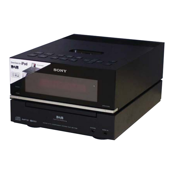
• HCD-BX77DBi is the amplifier, CD player, tuner
and iPod section in CMT-BX77DBi.
iPod is a trademark of Apple Inc., registered in the U.S.
and other countries.
MPEG Layer-3 audio coding technology and patents
licensed from Fraunhofer IIS and Thomson.
All other trademarks and registered trademarks are of
their respective holders. In this manual,
are not specified.
Note: Refer to supplement-1 for SPECIFICATIONS of the following serial No. or larger.
AEP model : Serial No. 5100859 or larger
UK model : Serial No. 6123118 or larger
Amplifier section
DIN power output (rated):
18 watts + 18 watts (6 ohms at 1 kHz, DIN)
Continuous RMS power output (reference): 25 watts + 25 watts (6 ohms at
1 kHz, 10% THD)
Music power output (reference): 38 watts + 38 watts (6 ohms at 1 kHz, 10%
THD)
Inputs
AUDIO IN (stereo mini jack): voltage 250 mV, impedance 47 kilohms
Outputs
PHONES (stereo mini jack): accepts headphones of 8 ohms or more
SPEAKER: accepts impedance of 6 to 16 ohms
CD player section
System: Compact disc and digital audio system
Laser Diode Properties
Emission Duration: Continuous
Laser Output*: Less than 44.6 μW
* This output is the value measurement at a distance of 200 mm from the
objective lens surface on the Optical Pick-up Block with 7 mm aperture.
Frequency response: 20 Hz
Signal-to-noise ratio: More than 90 dB
Dynamic range: More than 90 dB
Tuner section
DAB tuner section:
Frequency range*
Band-III: 174.928 (5A) MHz
* For details, see "DAB frequency table" below.
Antenna: FM/DAB lead antenna
Antenna terminal: 75 ohms, F female
FM stereo, FM/AM superheterodyne tuner
FM tuner section:
Tuning range: 87.5 MHz
Antenna: FM/DAB lead antenna
Antenna terminals: 75 ohms unbalanced
Intermediate frequency: 10.7 MHz
AM tuner section:
Tuning range: 531 kHz
Antenna: AM loop antenna, external antenna terminal
Intermediate frequency: 450 kHz
9-889-832-03
Sony Corporation
2011E05-1
©
2011.05
Published by Sony Techno Create Corporation
HCD-BX77DBi
TM
and ® marks
SPECIFICATIONS
20 kHz
239.200 (13F) MHz
108.0 MHz (50 kHz step)
1,602 kHz (9 kHz step)
Model Name Using Similar Mechanism
Base Unit Name
Optical Pick-up Name
DAB frequency table (Band-III)
Frequency
Label
Frequency
174.928 MHz
5A
209.936 MHz
176.640 MHz
5B
211.648 MHz
178.352 MHz
5C
213.360 MHz
180.064 MHz
5D
215.072 MHz
181.936 MHz
6A
216.928 MHz
183.648 MHz
6B
218.640 MHz
185.360 MHz
6C
220.352 MHz
187.072 MHz
6D
222.064 MHz
188.928 MHz
7A
223.936 MHz
190.640 MHz
7B
225.648 MHz
192.352 MHz
7C
227.360 MHz
194.064 MHz
7D
229.072 MHz
195.936 MHz
8A
230.784 MHz
197.648 MHz
8B
232.496 MHz
199.360 MHz
8C
234.208 MHz
201.072 MHz
8D
235.776 MHz
202.928 MHz
9A
237.488 MHz
204.640 MHz
9B
239.200 MHz
206.352 MHz
9C
208.064 MHz
9D
COMPACT DISC RECEIVER
AEP Model
UK Model
HCD-BX70DBi
BU-K6BD90-WOD
KSM-213DCP
Label
10A
10B
10C
10D
11A
11B
11C
11D
12A
12B
12C
12D
13A
13B
13C
13D
13E
13F
– Continued on next page –
Advertisement
Table of Contents

Related Manuals for Sony HCD-BX77DBi


Summary of Contents for Sony HCD-BX77DBi
- Page 1 HCD-BX77DBi SERVICE MANUAL AEP Model UK Model Ver. 1.2 2011.05 • HCD-BX77DBi is the amplifier, CD player, tuner and iPod section in CMT-BX77DBi. iPod is a trademark of Apple Inc., registered in the U.S. Model Name Using Similar Mechanism HCD-BX70DBi and other countries.
-
Page 2: Table Of Contents
COMPONENTS IDENTIFIED BY MARK 0 OR DOTTED LINE WITH MARK 0 ON THE SCHEMATIC DIAGRAMS AND IN THE PARTS LIST ARE CRITICAL TO SAFE OPERATION. REPLACE THESE COMPONENTS WITH SONY PARTS WHOSE PART NUMBERS APPEAR AS SHOWN IN THIS MANUAL OR IN SUPPLEMENTS PUBLISHED BY SONY. -
Page 3: Servicing Notes
HCD-BX77DBi SECTION 1 SERVICING NOTES UNLEADED SOLDER NOTES ON HANDLING THE OPTICAL PICK-UP Boards requiring use of unleaded solder are printed with the lead- BLOCK OR BASE UNIT free mark (LF) indicating the solder contains no lead. (Caution: Some printed circuit boards may not come printed with... -
Page 4: Disassembly
HCD-BX77DBi SECTION 2 DISASSEMBLY • This set can be disassembled in the order shown below. 2-1. DISASSEMBLY FLOW 2-2. PANEL (SIDE L/R) (Page 5) 2-3. TOP PANEL BLOCK (Page 5) 2-5. FRONT PANEL BLOCK 2-6. REAR PANEL BLOCK 2-4. TOP KEY BOARD, 2-11. -
Page 5: Panel (Side L/R)
HCD-BX77DBi Note: Follow the disassembly procedure in the numerical order given. 2-2. PANEL (SIDE L/R) 2 screw (BVTP3 3 panel (side L) 2 screw (BVTP3 1 two screws (BVTP S3 3 panel (side R) 1 two screws (BVTP S3 2-3. -
Page 6: Top Key Board, Ip Board, Panel Top (Ip)
HCD-BX77DBi 2-4. TOP KEY BOARD, IP BOARD, PANEL TOP (IP) qh panel top (IP) 7 button (function) 6 button (function B) qg base (IP) assy 5 button (tune) qf four screws 4 button (enter) (BVTP2.6 ) qs connector (CN101) 2 TOP KEY board... -
Page 7: Rear Panel Block
HCD-BX77DBi 2-6. REAR PANEL BLOCK 5 rear panel block 1 flexible flat cable (11 core) (CN310) 3 two screws (BVTP3 4 three screws (BVTP S3 2 fan motor connector (CN313) 2-7. PANEL (REAR) 1 two screws (BVTP3 8 panel (rear) -
Page 8: Amp Board Block
HCD-BX77DBi 2-8. AMP BOARD BLOCK 4 two screws (BV3) 1 flexible flat cable (7 core) (AMP board: CN308/MAIN board: CN309) 5 AMP board block 2 connector (CN312) 3 connector (CN320) 2-9. POWER BOARD BLOCK 6 four screws (BV SUMITITE S 4... -
Page 9: Main Board
HCD-BX77DBi 2-10. MAIN BOARD 3 flexible flat cable (11 core) (CN326) 2 flexible flat cable (21 core) (CN305) 4 connector (CN316) 5 connector (CN904) 1 flexible flat cable (5P) (CN311) 6 two screws (BVTT3 7 MAIN board 2-11. DAB BOARD, MODULE (DAB TUNER) -
Page 10: Loading Mechanism Block
HCD-BX77DBi 2-12. LOADING MECHANISM BLOCK 3 two screws (BVTP2.6) 4 holder (CD) 5 three screws (BV3) 0 loading mechanism block 9 door CD 8 flexible flat cable (5 core) (CN001) 1 flexible flat cable (21 core) (CN305) 7 flexible flat cable (21 core) -
Page 11: Belt
HCD-BX77DBi 2-14. BELT 5 belt belt 3 claw 3 claw 4 tray (AU) 1 Slide the boss in the direction of the arrow. 2-15. OPTICAL PICK-UP BLOCK (KSM-213DCP) Note 1: When disconnecting the wire (fl at type) (16 core) of optical pick-up block, solder the short-land. -
Page 12: Test Mode
HCD-BX77DBi SECTION 3 TEST MODE COLD RESET CD SHIP MODE The cold reset clears all data including preset data stored in the This mode moves the optical pick-up to the position durable to RAM to initial conditions. Execute this mode when returning the vibration. - Page 13 HCD-BX77DBi CD SERVICE MODE This mode can run the CD sled motor freely. Use this mode, for instance, when cleaning the optical pick-up. Procedure: 1. Press the [ ] button to turn the power on. 2. Press the [FUNCTION] button to select “CD”.
-
Page 14: Electrical Checks
HCD-BX77DBi SECTION 4 ELECTRICAL CHECKS CD SECTION TUNER SECTION FM TUNE LEVEL CHECK Note: 1. CD Block is basically constructed to operate without adjust- ment. signal generator 2. Use YEDS-18 disc (Part No. 3-702-101-01) unless otherwise indicated. 3. Use an oscilloscope with more than 10 MΩ impedance. -
Page 15: Diagrams
HCD-BX77DBi SECTION 5 DIAGRAMS 5-1. BLOCK DIAGRAM - CD SERVO Section - AVDD DETECTOR +3.3V FNi1 (A) 97 FPi1 (B) CD-L (Page 17) AGCi RFEQo 81 RFi 94 FNi2 (C) 82 RFRPi R-CH 96 FPi2 (D) RFRP RFZI 100 TNi (E) -
Page 16: Block Diagram - Ipod, Tuner, Dab Section
HCD-BX77DBi 5-2. BLOCK DIAGRAM - iPod, TUNER, DAB Section - CN102 (iPod) iPod-L L-CH LINE AMP LINE-OUT-L IC303 (Page 17) R-CH LINE-OUT-R MUTING R-ch is omitted due to same as L-ch. Q103, 105 SIGNAL PATH : TUNER (FM/AM) MUTING iPod INTERFACE... -
Page 17: Block Diagram - Main Section
HCD-BX77DBi 5-3. BLOCK DIAGRAM - MAIN Section - J301 R-CH AUDIO IN CD-L (Page 15) INPUT SELECTOR IC312 DAB-L (Page 16) INPUT SELECTOR, TUNER-L ELECTRICAL VOLUME, SURROUND/TONE CONTROL (Page 16) IC304 Q320 Q319 iPod-L (Page 16) POWER AMP SEL1 IC601... -
Page 18: Block Diagram - Panel, Power Supply Section
HCD-BX77DBi 5-4. BLOCK DIAGRAM - PANEL, POWER SUPPLY Section - T801 DC/DC CONVERTER FL901 FLUORESCENT RECT INDICATOR TUBE D904, 905 PROTECT (Page 17) Q903 GRID DRIVE T901 Q905 MAIN POWER TRANSFORMER 59, 60 1 – 31, 61 – 64 33 – 42... - Page 19 HCD-BX77DBi THIS NOTE IS COMMON FOR PRINTED WIRING BOARDS AND SCHEMATIC DIAGRAMS. • Circuit Boards Location. (In addition to this, the necessary note is printed in each block.) For Printed Wiring Boards. For Schematic Diagrams. Note: Note: • X : Parts extracted from the component side.
-
Page 20: Printed Wiring Boards - Cd Section
HCD-BX77DBi 5-5. PRINTED WIRING BOARDS - CD Section - • See page 19 for Circuit Boards Location. • : Uses unleaded solder. CD BOARD (CONDUCTOR SIDE) CD BOARD (COMPONENT SIDE) M401 (SPINDLE) S201 (LIMIT) C404 C403 R402 IC401 TP124 M402... -
Page 21: Schematic Diagram - Cd Board
HCD-BX77DBi 5-6. SCHEMATIC DIAGRAM - CD Board - • See page 22 for Waveforms. • See page 36 for IC Block Diagrams. • See page 38 for IC Pin Function Description. R127 C107 R126 C136 R125 R142 R139 R129 Q301... -
Page 22: Printed Wiring Board - Dab Board
HCD-BX77DBi • Waveforms 5-7. PRINTED WIRING BOARD - DAB Board - • See page 19 for Circuit Boards Location. • : Uses unleaded solder. – CD Board – – IP Board – – PANEL Board – IC101 ia (RFi) IC101 9 (XOUT) IC902 t;... -
Page 23: Schematic Diagram - Dab Board
HCD-BX77DBi 5-8. SCHEMATIC DIAGRAM - DAB Board - • See page 36 for IC Block Diagrams. C833 C811 R825 R803 R807 220p 4.7k R805 R811 C817 ANTENNA DAB 75 DAB TUNER MODULE C818 CN800 LINE AMP IC803 NJM4558M- C834 R813... -
Page 24: Printed Wiring Board - Ip Board
HCD-BX77DBi Ver. 1.1 5-9. PRINTED WIRING BOARD - IP Board - • See page 19 for Circuit Boards Location. • : Uses unleaded solder. IP BOARD IP BOARD (SIDE A) (SIDE B) R105 C102 IC103 C105 R135 IC102 C109 R122... -
Page 25: Schematic Diagram - Ip Board
HCD-BX77DBi Ver. 1.1 5-10. SCHEMATIC DIAGRAM - IP Board - • See page 22 for Waveforms. • See page 36 for IC Block Diagrams. • See page 38 for IC Pin Function Description. IP BOARD IC B/D CN102 (iPod) IC102... -
Page 26: Printed Wiring Boards - Main Section
HCD-BX77DBi 5-11. PRINTED WIRING BOARDS - MAIN Section - • See page 19 for Circuit Boards Location. • : Uses unleaded solder. ANTENNA FM 75 COAXIAL M901 (Page 20) (Page 24) (Page 22) TUNER (FM/AM) (FAN) SUPPLIED WITH THE CD BOARD... -
Page 27: Schematic Diagram - Main Section (1/3)
HCD-BX77DBi 5-12. SCHEMATIC DIAGRAM - MAIN Section (1/3) - • See page 36 for IC Block Diagrams. R201 (1/3) 2.2k JR201 R-IN AGND R101 2.2k JR101 L-IN C116 C216 STBY C368 R117 R217 ±PRE C369 C367 R109 R209 4.7k 4.7k... -
Page 28: Schematic Diagram - Main Section (2/3)
HCD-BX77DBi 5-13. SCHEMATIC DIAGRAM - MAIN Section (2/3) - • See page 22 for Waveforms. • See page 36 for IC Block Diagrams. • See page 38 for IC Pin Function Description. (Page 27) (2/3) C362 C498 R487 R473 R485... -
Page 29: Schematic Diagram - Main Section (3/3)
HCD-BX77DBi 5-14. SCHEMATIC DIAGRAM - MAIN Section (3/3) - • See page 36 for IC Block Diagrams. (Page 27) (Page 25) (Page 27) (Page (3/3) CLP311 EP301 CN325 CN326 IC307 KIA7809API-U/PF R431 R419 C365 C359 (CHASSIS) D329 MA2J1110GLS0 CN316 REGULATOR... -
Page 30: Printed Wiring Boards - Amp, Headphone Section
HCD-BX77DBi 5-15. PRINTED WIRING BOARDS - AMP, HEADPHONE Section - • See page 19 for Circuit Boards Location. • : Uses unleaded solder. (Page 26) (Page 26) MAIN BOARD MAIN BOARD CN309 CN321 AMP BOARD C515 C522 C521 (CHASSIS) (CHASSIS) -
Page 31: Schematic Diagram - Amp, Headphone Section
HCD-BX77DBi 5-16. SCHEMATIC DIAGRAM - AMP, HEADPHONE Section - • See page 36 for IC Block Diagrams. IC601 STK433-730-E POWER AMP R502 C502 R505 C504 470p 470p CN308 C511 R501 R521 C501 C505 R-IN 100p 100p C512 R506 R522 10 50V... -
Page 32: Printed Wiring Boards - Panel Section
HCD-BX77DBi 5-17. PRINTED WIRING BOARDS - PANEL Section - • See page 19 for Circuit Boards Location. • : Uses unleaded solder. PANEL BOARD C812 R933 T801 R930 DC/DC CONVERTER R919 R932 C814 Q903 FL901 R920 C811 JW812 Q905 FLUORESCENT INDICATOR TUBE... -
Page 33: Schematic Diagram - Panel Section
HCD-BX77DBi 5-18. SCHEMATIC DIAGRAM - PANEL Section - • See page 22 for Waveforms. • See page 36 for IC Block Diagrams. (Page CN802 TUNER/ iPod BAND AUDIO IN R856 R855 R854 R853 4.7k 2.2k FL901 S804 S807 S806 S805... -
Page 34: Printed Wiring Board - Power Board
HCD-BX77DBi 5-19. PRINTED WIRING BOARD - POWER Board - • See page 19 for Circuit Boards Location. • : Uses unleaded solder. POWER BOARD SUB POWER D906 TRANSFORMER (AC IN) LINE FILTER (Page 26) MAIN BOARD CN303 NOT REPLACEABLE: BUILT IN TRANSFORMER... -
Page 35: Schematic Diagram - Power Board
HCD-BX77DBi 5-20. SCHEMATIC DIAGRAM - POWER Board - D923 MC2838 D922 MA2J1110GLS0 C914 R905 R904 R906 4.7k 4.7k C921 R909 R908 R910 R911 1000 T902 TRANSFORMER D908 MC2838 CN904 D907 USB UNREG GND MC2836 USB UNREG RELAY SUB GND UNREG SUB... - Page 36 HCD-BX77DBi • IC Block Diagrams – IP Board – – MAIN Board – – CD Board – IC102 TK11133CSCL-G IC201 R5523N001B-TR-F IC401 BA5826HFP-E2 IC201 TK63115SCL-G@GT 5 OUT VIN 1 VO1(–) D.BUFF THERMAL & GATE CURRENT VO4(–) OVER CURRENT CONTROL LIMIT VO1(+) D.BUFF...
- Page 37 HCD-BX77DBi – AMP Board – IC601 STK433-730-E PRE DRIVE FINAL DRIVE PRE DRIVE FINAL DRIVE STANDBY CIRCUIT – PANEL Board – IC902 PT6302LQ-010 VSS 49 OSCI 50 OSCILLATOR OSCO 51 TIMING TIMING RSTB 52 GENERATOR 1 GENERATOR 2 SG35 DUTY CONTROL...
- Page 38 HCD-BX77DBi • IC Pin Function Description CD BOARD IC101 TC94A70FG-006 (D, HZ (CD-MP3 PROCESSOR) Pin No. Pin Name Description AVSS3 Ground terminal RFZi RF ripple zero crossing signal input terminal RFRP RF ripple signal output terminal SBAD/RFDC Sub beam addition signal or RF peak detection signal output terminal...
- Page 39 HCD-BX77DBi Pin No. Pin Name Description Microcomputer interface mode selection signal input terminal Fixed at “H” in this set DOUT (PO6) Digital audio data output terminal Not used AOUT (PO7) Audio data output terminal Not used BCK (PO8) Bit clock signal output terminal...
- Page 40 HCD-BX77DBi IP BOARD IC101 R5F21246SN060FP (iPod INTERFACE) Pin No. Pin Name Description Not used Not used Not used Not used MODE Mode selection signal input terminal “L”: single chip mode, “H”: serial I/O mode, 6, 7 P34, P44 Not used...
- Page 41 HCD-BX77DBi MAIN BOARD IC301 R5F3640DDFAR (SYSTEM CONTROLLER) Pin No. Pin Name Description CD BUS2 to CD 1 to 3 Serial data output to the CD-MP3 processor BUS0 SIRCS SIRCS signal input from the remote control receiver STBY-RELAY Power on/off control signal output terminal “H”: power on...
- Page 42 HCD-BX77DBi Pin No. Pin Name Description Power supply terminal (+3.3V) Not used Ground terminal Not used I-POWER MONITOR Power monitor input terminal DEC BUS SEL Bus selection signal output terminal Not used MP3 IREQ Request signal input from the CD-MP3 processor...
-
Page 43: Exploded Views
HCD-BX77DBi SECTION 6 EXPLODED VIEWS Note: • -XX and -X mean standardized parts, so • The mechanical parts with no reference The components identifi ed by mark 0 they may have some difference from the number in the exploded views are not sup- or dotted line with mark 0 are critical for original one. -
Page 44: Top Panel Section
HCD-BX77DBi Ver. 1.1 6-2. TOP PANEL SECTION not supplied not supplied (TOP KEY board) not supplied (HOLD board) Note: (Former) AEP model : Serial No. 5100858 or smaller UK model : Serial No. 6123117 or smaller (New) AEP model : Serial No. 5100859 or larger UK model : Serial No. -
Page 45: Front Panel Section
HCD-BX77DBi 6-3. FRONT PANEL SECTION not supplied (PANEL board) not supplied FL901 Ref. No. Part No. Description Remark Ref. No. Part No. Description Remark A-1772-933-A PANEL ASSY, FRONT 1-831-997-21 CABLE, FLEXIBLE FLAT (13 CORE) 4-233-372-02 FOOT (FELT) FL901 1-519-993-21 INDICATOR TUBE, FLUORESCENT 3-087-053-01 +BVTP2.6 (3CR) -
Page 46: Main Board Section
HCD-BX77DBi 6-4. MAIN BOARD SECTION not supplied (GUARD board) not supplied not supplied (AMP board) M901 supplied not supplied (5VREG board) not supplied (9VREG board) supplied POWER board section Ref. No. Part No. Description Remark Ref. No. Part No. Description... -
Page 47: Power Board Section
HCD-BX77DBi 6-5. POWER BOARD SECTION F902 not supplied F901 (POWER board) not supplied T901 not supplied not supplied not supplied not supplied not supplied (HP board) loading mechanism section not supplied Ref. No. Part No. Description Remark Ref. No. Part No. -
Page 48: Loading Mechanism Section
HCD-BX77DBi 6-6. LOADING MECHANISM SECTION not supplied not supplied (MOTOR board) not supplied base unit section Ref. No. Part No. Description Remark Ref. No. Part No. Description Remark A-1242-967-B LOADING (BK) ASSY 4-156-130-01 SPRING, CONE 3-080-478-01 BELT 4-229-005-41 INSULATOR 4-985-672-01... -
Page 49: Base Unit Section (Bu-K6Bd90-Wod)
HCD-BX77DBi 6-7. BASE UNIT SECTION (BU-K6BD90-WOD) (including sled motor (M402), spindle motor (M401)) spindle motor (M401) sled motor (M402) S201 Ref. No. Part No. Description Remark Ref. No. Part No. Description Remark A-1217-914-A CD BOARD, COMPLETE 0 301 A-4735-357-A OPTICAL PICK-UP BLOCK (KSM-213D) -
Page 50: Electrical Parts List
HCD-BX77DBi SECTION 7 5VREG 9VREG ELECTRICAL PARTS LIST Note: • Due to standardization, replacements in • CAPACITORS When indicating parts by reference num- the parts list may be different from the uF: μF ber, please include the board name. parts specifi ed in the diagrams or the com- •... - Page 51 HCD-BX77DBi Ref. No. Part No. Description Remark Ref. No. Part No. Description Remark R544 1-216-853-11 METAL CHIP 470K 1/10W C206 1-165-908-11 CERAMIC CHIP 1uF C207 1-165-908-11 CERAMIC CHIP 1uF R545 1-216-833-11 METAL CHIP 1/10W C301 1-164-360-11 CERAMIC CHIP 0.1uF R546...
- Page 52 HCD-BX77DBi Ref. No. Part No. Description Remark Ref. No. Part No. Description Remark R153 1-216-857-11 METAL CHIP 1/10W C828 1-126-929-11 ELECT 4700uF R154 1-216-857-11 METAL CHIP 1/10W C833 1-126-160-11 ELECT R155 1-216-805-11 METAL CHIP 1/10W C834 1-126-160-11 ELECT R156 1-216-809-11...
- Page 53 HCD-BX77DBi Ver. 1.1 MAIN Ref. No. Part No. Description Remark Ref. No. Part No. Description Remark < RESISTOR > Q103 6-551-750-01 TRANSISTOR 2SD2114KT146W Q104 6-551-750-01 TRANSISTOR 2SD2114KT146W R132 1-216-841-11 METAL CHIP 1/10W Q105 6-551-750-01 TRANSISTOR 2SD2114KT146W R133 1-216-821-11 METAL CHIP...
- Page 54 HCD-BX77DBi MAIN Ref. No. Part No. Description Remark Ref. No. Part No. Description Remark C120 1-126-960-11 ELECT C366 1-164-156-11 CERAMIC CHIP 0.1uF C122 1-100-597-91 CERAMIC CHIP 0.1uF C367 1-126-935-11 ELECT 470uF C123 1-162-974-11 CERAMIC CHIP 0.01uF C368 1-164-156-11 CERAMIC CHIP 0.1uF...
- Page 55 HCD-BX77DBi MAIN Ref. No. Part No. Description Remark Ref. No. Part No. Description Remark IC304 6-712-055-01 IC BD3499FV-E2 IC307 6-713-032-01 IC KIA7809API-U/PF JR498 1-216-864-11 SHORT CHIP IC310 6-702-038-11 IC PST3628NR < COIL > IC311 8-759-598-69 IC BA6956AN IC312 8-759-430-37 IC MC14052BDTR2...
- Page 56 HCD-BX77DBi MAIN Ref. No. Part No. Description Remark Ref. No. Part No. Description Remark R131 1-216-837-11 METAL CHIP 1/10W R413 1-216-841-11 METAL CHIP 1/10W R134 1-216-829-11 METAL CHIP 4.7K 1/10W R414 1-216-805-11 METAL CHIP 1/10W R153 1-260-304-51 CARBON 1/2W R415...
- Page 57 HCD-BX77DBi MAIN MOTOR PANEL Ref. No. Part No. Description Remark Ref. No. Part No. Description Remark R611 1-216-829-11 METAL CHIP 4.7K 1/10W X302 1-814-062-21 VIBRATOR, CERAMIC (5MHz) R700 1-216-809-11 METAL CHIP 1/10W ************************************************************ R701 1-216-809-11 METAL CHIP 1/10W R702 1-216-809-11...
- Page 58 HCD-BX77DBi PANEL POWER TOP KEY Ref. No. Part No. Description Remark Ref. No. Part No. Description Remark < RESISTOR > D919 6-501-569-01 DIODE 1N5401-C352 D920 6-500-335-01 DIODE MC2838-T112-1 R851 1-216-821-11 METAL CHIP 1/10W D922 6-501-817-01 DIODE MA2J1110GLS0 R852 1-216-825-11 METAL CHIP 2.2K...
- Page 59 HCD-BX77DBi TOP KEY Ref. No. Part No. Description Remark S807 1-762-875-21 SWITCH, KEYBOARD (TUNER/BAND) S809 1-762-875-21 SWITCH, KEYBOARD (DAB AUTOSCAN) S810 1-762-875-21 SWITCH, KEYBOARD (DSGX) S811 1-762-875-21 SWITCH, KEYBOARD ( x CANSEL) S812 1-762-875-21 SWITCH, KEYBOARD (FUNCTION) S813 1-762-875-21 SWITCH, KEYBOARD (FOLDER +)
- Page 60 HCD-BX77DBi MEMO...
- Page 61 HCD-BX77DBi AEP Model UK Model SERVICE MANUAL Ver. 1.1 2010.08 SUPPLEMENT-1 File this supplement with the service manual. Subject: Change of IP board to corresponded for new iPod series In this set, to correspond to new model iPod, the IP board has been changed in the midway of production.
- Page 62 HCD-BX77DBi 2. SPECIFICATIONS iPod section Main unit Compatible iPod models*: Amplifier section * Update your iPod to use the latest software before you use it. DIN power output (rated): 18 watts + 18 watts (6 ohms at 1 kHz, DIN)
- Page 63 HCD-BX77DBi Ver. 1.2 3. DIAGRAMS THIS NOTE IS COMMON FOR PRINTED WIRING BOARDS AND SCHEMATIC DIAGRAMS. (In addition to this, the necessary note is printed in each block.) For Printed Wiring Boards. For Schematic Diagrams. Note: Note: • : Internal component.
- Page 64 HCD-BX77DBi Ver. 1.2 3-2. SCHEMATIC DIAGRAM - IP Board - IP BOARD CN102 (iPod) IC102 CL109 R110 100k TK11133CSCL-G DGND R108 100k IC103 DGND CONT CL150 R107 100k TPA+ RESET SIGNAL GENERATOR CL103 USB D+ VOUT CL149 R109 100k IC103...
- Page 65 HCD-BX77DBi Ver. 1.2 4. ELECTRICAL PARTS LIST Note: • Due to standardization, replacements in • CAPACITORS When indicating parts by reference num- the parts list may be different from the uF: μF ber, please include the board name. parts specifi ed in the diagrams or the com- •...
- Page 66 HCD-BX77DBi REVISION HISTORY Checking the version allows you to jump to the revised page. Also, clicking the version at the top of the revised page allows you to jump to the next revised page. Ver. Date Description of Revision 2010.04 2010.08...