
Related Manuals for Asus Aaeon GENESYS-WHU6


Summary of Contents for Asus Aaeon GENESYS-WHU6
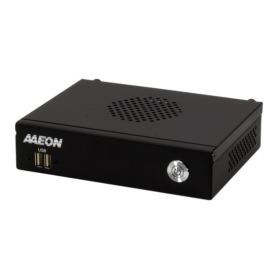
- Page 1 GENESYS-WHU6 GENESYS Compact Embedded System User’s Manual 1 Last Updated: March 16, 2021...
- Page 2 Copyright Notice This document is copyrighted, 2021. All rights are reserved. The original manufacturer reserves the right to make improvements to the products described in this manual at any time without notice. No part of this manual may be reproduced, copied, translated, or transmitted in any form or by any means without the prior written permission of the original manufacturer.
- Page 3 Acknowledgement All other products’ name or trademarks are properties of their respective owners. Microsoft Windows is a registered trademark of Microsoft Corp. ⚫ Intel®, Pentium®, and Celeron® are registered trademarks of Intel Corporation ⚫ Intel Core™ is a trademark of Intel Corporation ⚫...
- Page 4 Packing List Before setting up your product, please make sure the following items have been shipped: Item Quantity GENESYS-WHU6 If any of these items are missing or damaged, please contact your distributor or sales representative immediately. Preface...
- Page 5 About this Document This User’s Manual contains all the essential information, such as detailed descriptions and explanations on the product’s hardware and software features (if any), its specifications, dimensions, jumper/connector settings/definitions, and driver installation instructions (if any), to facilitate users in setting up their product. Users may refer to the product page at AAEON.com for the latest version of this document.
- Page 6 Safety Precautions Please read the following safety instructions carefully. It is advised that you keep this manual for future references All cautions and warnings on the device should be noted. Make sure the power source matches the power rating of the device. Position the power cord so that people cannot step on it.
- Page 7 If any of the following situations arises, please the contact our service personnel: Damaged power cord or plug Liquid intrusion to the device iii. Exposure to moisture Device is not working as expected or in a manner as described in this manual The device is dropped or damaged Any obvious signs of damage displayed on the device...
- Page 8 FCC Statement This device complies with Part 15 FCC Rules. Operation is subject to the following two conditions: (1) this device may not cause harmful interference, and (2) this device must accept any interference received including interference that may cause undesired operation.
- Page 9 China RoHS Requirements (CN) 产品中有毒有害物质或元素名称及含量 AAEON Main Board/ Daughter Board/ Backplane 有毒有害物质或元素 部件名称 铅 汞 镉 六价铬 多溴联苯 多溴二苯醚 (Pb) (Hg) (Cd) (Cr(VI)) (PBB) (PBDE) 印刷电路板 ○ ○ ○ ○ ○ ○ 及其电子组件 外部信号 ○ ○ ○ ○ ○ ○ 连接器及线材...
- Page 10 China RoHS Requirement (EN) Poisonous or Hazardous Substances or Elements in Products AAEON Main Board/ Daughter Board/ Backplane Poisonous or Hazardous Substances or Elements Hexavalent Polybrominated Polybrominated Component Lead Mercury Cadmium Chromium Biphenyls Diphenyl Ethers (Pb) (Hg) (Cd) (Cr(VI)) (PBB) (PBDE) PCB &...
-
Page 11: Table Of Contents
Table of Contents Chapter 1 - Product Specifications..................1 Specifications ......................2 Chapter 2 – Hardware Information ..................5 Dimensions ....................... 6 Jumpers and Connectors ..................8 List of Jumpers ......................9 2.3.1 Front Panel Connector (JP1) ................. 9 2.3.2 COM2 Pin8 Function Selection (JP3) ............ - Page 12 2.4.16 Nano SIM Card Socket (CN20) ..............24 2.4.17 CPU Fan (CN22) ................... 25 2.4.18 Battery Connector (CN23) ................. 25 2.4.19 LAN (RJ-45) Port 1/Port 2 (CN24/CN25) ..........26 2.4.20 USB 3.2 Gen 2 Ports 0 & 1 (CN26) ............27 2.4.21 USB 3.2 Gen 2 Ports 2 &...
- Page 13 3.4.5 Advanced: SIO Configuration ..............57 3.4.5.1 Serial Port 1 Configuration .............. 58 3.4.5.2 Serial Port 2 Configuration ............. 59 3.4.6 Advanced: Power Management ............... 60 Setup Submenu: Chipset ..................61 3.5.1 Chipset: System Agent (SA) Configuration ..........62 3.5.2 Chipset: PCH IO Configuration ..............
-
Page 14: Chapter 1 - Product Specifications
Chapter 1 Chapter 1 - Product Specifications... -
Page 15: Specifications
Specifications System Form Factor 3.5" Subcompact Board System Intel® 8th Generation Core™ i7/i5/i3/Celeron i7-8665UE (4C, 1.7GHz, up to 4.4GHz) i5-8365UE (4C, 1.6GHz, up to 4.1GHz) i3-8145UE (2C, 2.2GHz, up to 3.9GHz) Celeron 4305UE (2C, 2GHz) CPU Frequency Up to 4.4GHz Chipset 8th Generation Intel®... - Page 16 Display VGA/LCD Controller Intel® 8th Generation Core™ i7/i5/i3/Celeron Video Output VGA x 1 HDMI 2.0 x 1 Backlight inverter supply — Ethernet Intel® i210/i211 & i219, 10/100/1000Base, RJ 45 x2 Audio High Definition Audio Interface (Optional) USB Port USB 3.2 Gen 2 x 4 USB 2.0 x 2 Serial Port RS-232/422/485 x 2...
- Page 17 Touch — Chapter 1 – Product Specifications...
-
Page 18: Chapter 2 - Hardware Information
Chapter 2 Chapter 2 – Hardware Information... -
Page 19: Dimensions
Dimensions GENESYS-WHU6 System View Chapter 2 – Hardware Information... - Page 20 GENE-WHU6 Board Chapter 2 – Hardware Information...
-
Page 21: Jumpers And Connectors
Jumpers and Connectors Chapter 2 – Hardware Information... -
Page 22: List Of Jumpers
List of Jumpers Please refer to the table below for all of the board’s jumpers that you can configure for your application Label Function Front Panel Connector COM2 Pin8 Function Selection Clear CMOS Jumper JP10 Auto Power Button Enable/Disable Selection 2.3.1 Front Panel Connector (JP1) Function... -
Page 23: Com2 Pin8 Function Selection (Jp3)
2.3.2 COM2 Pin8 Function Selection (JP3) Ring (Default) +12V 2.3.3 Clear CMOS Jumper (JP9) Normal (Default) Clear CMOS 2.3.4 Auto Power Button Enable/Disable Selection (JP10) 1 2 3 Disable/ATX (Default) Enable/AT Note: When disabled, use Power Button JP10 (pins 1-2) to power on the system. Chapter 2 –... -
Page 24: List Of Connectors
List of Connectors Please refer to the table below for all of the board’s connectors that you can configure for your application Label Function +5V Output for SATA HDD SATA Port External Power Input Audio I/O Port External +5VSB Input DDR4 SO-DIMM Slot COM Port 1 RS-232/422/485 COM Port 2 RS-232/422/485... -
Page 25: Output For Sata Hdd (Cn1)
Label Function CN29 VGA Port CN30 M.2 B-Key 2280 CN31 LAN SDP CONN 2.4.1 +5V Output for SATA HDD (CN1) Pin Name Signal Type Signal Level +5V at 1A 2.4.2 SATA Port (CN2) Pin 1 Pin 7 Pin Name Signal Type Signal Level SATA_TX+ DIFF... -
Page 26: External Power Input (Cn3)
2.4.3 External Power Input (CN3) Pin Name Signal Type Signal Level +12V +9~+36V (or +12V) Note: There are two types of power input, 9~36V or 12V only; by BOM change. 2.4.4 Audio I/O Port (CN5) MIC_L MIC_R GND_AUDIO LINE_L_IN LINE_R_IN GND_AUDIO LEFT_OUT GND_AUDIO... -
Page 27: External +5Vsb Input (Cn6)
Pin Name Signal Type Signal Level GND_AUDIO RIGHT_OUT +5V_AUDIO 2.4.5 External +5VSB Input (CN6) Pin Name Signal Type Signal Level PS_ON# +5VSB 2.4.6 DDR SO-DIMM Slot (CN7) Standard Specifications Chapter 2 – Hardware Information... -
Page 28: Com Port 1 (Cn8)
2.4.7 COM Port 1 (CN8) RS-232 Pin Name Signal Type Signal Level DCD1 DSR1 RTS1 ±5V ±5V CTS1 DTR1 ±5V Chapter 2 – Hardware Information... - Page 29 RS-485 Pin Name Signal Type Signal Level RS485_ D- ±5V RS485_D+ ±5V RS-422 Pin Name Signal Type Signal Level RS422_TX- ±5V RS422_TX+ ±5V RS422_RX+ RS422_RX- Chapter 2 – Hardware Information...
-
Page 30: Com Port 2 (Cn9)
2.4.8 COM Port 2 (CN9) RS-232 Pin Name Signal Type Signal Level DCD2 DSR2 RTS2 ±5V ±5V CTS2 DTR2 ±5V Chapter 2 – Hardware Information... - Page 31 RS-485 Pin Name Signal Type Signal Level RS485_ D2- ±5V RS485_D2+ ±5V NC/+5V/+12V +5V/+12V at 0.5A RS-422 Pin Name Signal Type Signal Level RS422_TX2- ±5V RS422_TX2+ ±5V RS422_RX2+ RS422_RX2- NC/+5V/+12V +5V/+12V at 0.5A Note 1: COM2 RS-232/422/485 can be set by BIOS setting. Default is RS-232. Note 2: Pin 8 function can be set by JP3 (See Ch 2.3.2).
-
Page 32: Mini-Card Slot (Full-Mini Card) (Cn10)
2.4.9 Mini-Card Slot (Full-Mini Card) (CN10) Pin Name Signal Type Signal level PCIE_WAKE# +3.3VSB +3.3V +1.5V +1.5V PCIE_CLK_REQ# UIM_PWR UIM_DATA PCIE_REF_CLK- DIFF UIM_CLK PCIE_REF_CLK+ DIFF UIM_RST UIM_VPP W_DISABLE# +3.3V PCIE_RST# +3.3V PCIE_RX- DIFF +3.3VSB +3.3V Chapter 2 – Hardware Information... - Page 33 Pin Name Signal Type Signal level PCIE_RX+ DIFF +1.5V +1.5V SMB_CLK +3.3V PCIE_TX- DIFF SMB_DATA +3.3V PCIE_TX+ DIFF USB_D- DIFF USB_D+ DIFF +3.3VSB +3.3V +3.3VSB +3.3V +1.5V +1.5V Chapter 2 – Hardware Information...
-
Page 34: Ddr So-Dimm Slot (Cn11)
Pin Name Signal Type Signal level +3.3VSB +3.3V 2.4.10 DDR SO-DIMM Slot (CN11) Standard Specifications 2.4.11 M.2 E-Key 2230 (CN12) Standard Specifications 2.4.12 USB 2.0 Port 5 (CN15) Pin Name Signal Type Signal Level +5VSB USB5_D- DIFF USB5_D+ DIFF Chapter 2 – Hardware Information... -
Page 35: Bios Debug Port (Cn16)
2.4.13 BIOS Debug Port (CN16) Pin Name Signal Type Signal Level SPI_MISO SPI_CLK +3.3VSB +3.3V SPI_MOSI SPI_CS Chapter 2 – Hardware Information... -
Page 36: Usb 2.0 Port 6 (Cn17)
2.4.14 USB 2.0 Port 6 (CN17) Pin Name Signal Type Signal Level +5VSB USB6_D- DIFF USB6_D+ DIFF G ND 2.4.15 LPC Port (CN18) Pin Name Signal Type Signal Level LAD0 +3.3V LAD1 +3.3V LAD2 +3.3V LAD3 +3.3V +3.3V +3.3V LFRAME# LRESET# +3.3V LCLK... -
Page 37: Nano Sim Card Socket (Cn20)
Pin Name Signal Type Signal Level SMB_CLK/I2C_CLK SMB_ALERT/SERIRQ +3.3V 2.4.16 Nano SIM Card Socket (CN20) Pin Name Signal Type Signal Level UIM_PWR UIM_RST UIM_CLK UIM_VPP UIM_DATA Chapter 2 – Hardware Information... -
Page 38: Cpu Fan (Cn22)
2.4.17 CPU Fan (CN22) Pin Name Signal Type Signal Level FAN_POWER +12V at 1A FAN_TAC 2.4.18 Battery Connector (CN23) Pin Name Signal Type Signal level +3.3V 3.3V Chapter 2 – Hardware Information... -
Page 39: Lan (Rj-45) Port 1/Port 2 (Cn24/Cn25)
2.4.19 LAN (RJ-45) Port 1/Port 2 (CN24/CN25) ACT/LINK SPEED Pin Name Signal Type Signal level MDI0+ DIFF MDI0- DIFF MDI1+ DIFF MDI2+ DIFF MDI2- DIFF MDI1- DIFF MDI3+ DIFF MDI3- DIFF Chapter 2 – Hardware Information... -
Page 40: Usb 3.2 Gen 2 Ports 0 & 1 (Cn26)
2.4.20 USB 3.2 Gen 2 Ports 0 & 1 (CN26) Pin Name Signal Type Signal Level +5VSB USB0_D- DIFF USB0_D+ DIFF USB0_SSRX− DIFF USB0_SSRX+ DIFF USB0_SSTX− DIFF USB0_SSTX+ DIFF +5VSB USB1_D- DIFF USB1_D+ DIFF USB1_SSRX− DIFF USB1_SSRX+ DIFF USB1_SSTX− DIFF USB1_SSTX+ DIFF Chapter 2 –... -
Page 41: Usb 3.2 Gen 2 Ports 2 & 3 (Cn27)
2.4.21 USB 3.2 Gen 2 Ports 2 & 3 (CN27) Pin Name Signal Type Signal Level +5VSB USB2_D- DIFF USB2_D+ DIFF USB2_SSRX− DIFF USB2_SSRX+ DIFF USB2_SSTX− DIFF USB2_SSTX+ DIFF +5VSB USB3_D- DIFF USB3_D+ DIFF USB3_SSRX− DIFF USB3_SSRX+ DIFF USB3_SSTX− DIFF USB3_SSTX+ DIFF Chapter 2 –... -
Page 42: Hdmi (Cn28)
2.4.22 HDMI (CN28) Pin Name Signal Type Signal Level HDMI_TX2+ DIFF HDMI_TX2- DIFF HDMI_TX1+ DIFF HDMI_TX1- DIFF HDMI_TX0+ DIFF HDMI_TX0- DIFF HDMI_CLK+ DIFF HDMI_CLK- DIFF DDC_CLK DDC_DATA HDMI_HPD Chapter 2 – Hardware Information... -
Page 43: Vga Port (Cn29)
2.4.23 VGA Port (CN29) Pin Name Signal Type Signal Level GREEN BLUE RED_GND_RTN GREEN_GND_RTN BLUE_GND_RTN DDC_DATA HSYNC VSYNC DDC_CLK 2.4.24 M.2 B-Key 2280 (CN30) Standard Specifications Chapter 2 – Hardware Information... -
Page 44: Lan Spd Connector (Cn31)
2.4.25 LAN SPD Connector (CN31) Pin Name Signal Type Signal Level SDP0 SDP1 SDP2 SDP3 Chapter 2 – Hardware Information... -
Page 45: Block Diagram
Block Diagram Chapter 2 – Hardware Information... -
Page 46: Hardware Installation
Hardware Installation This section details the steps needed to install various hardware components for the GENESYS-WHU6. It is recommended that you read through each step before beginning installation and to make sure you have all necessary tools and components. 2.6.1 Accessing the Bottom Panel For this process you will need a Philips head screwdriver. - Page 47 To reassemble the system, follow these steps in reverse order. Chapter 2 – Hardware Information...
-
Page 48: Ram Module Installation
2.6.2 RAM Module Installation Before you begin, make sure you have the RAM module(s) you wish to install ready. Memory Slot CN11 Memory Slot Step 1: Insert the RAM module in the DDR SO-DIMM Slot (CN11) at about 45° angle, then gently press down until it is secured by the tabs. -
Page 49: 2.5" Sata Drive Installation
2.6.3 2.5” SATA Drive Installation Before beginning, make sure you have the following prepared: 1 x SATA Drive 4 x Black Screws (to mount 2.5” drive) 1 x SATA Cable 1 x SATA Power Cable Phillips head screwdriver Please note the location of the SATA Port (CN2) and SATA Power connector (CN1) SATA Port SATA Power Step 1: Connect the SATA and SATA Power cables to the 2.5”... - Page 50 Step 2: Line up the mounting holes on the SATA drive with the four mounting points on the bottom panel. Note the orientation of the cables. Step 3: Secure the drive with four black mounting screws. Step 4: Insert the SATA Cable into CN2 and SATA Power Cable into CN1. If you are finished with hardware installation, replace the back panel and secure with two black screws.
-
Page 51: Com Port Installation
2.6.4 COM Port Installation Before beginning installation, please ensure you have the following: 2 x COM Port Connectors with cables 4 x jack standoffs (two included with each COM Port Connector) Phillips head screwdriver Note: This procedure will require opening both the top and bottom panels. Take care if you have already installed the 2.5”... - Page 52 Step 1: Hand loosen the spring mounted case screws securing the top panel to the rear panel of the system. The top panel will swing open towards the front panel. Step 2: Remove the COM Port knockouts by pushing with a finger or tool. Chapter 2 –...
- Page 53 Step 3: Fasten the COM Port Connectors to the appropriate knockouts using the four jack standoffs. Then, feed the cables around the side of the heatsink and board as shown. Chapter 2 – Hardware Information...
- Page 54 Step 4: Access the bottom side of the board. Carefully route the cables around the board and connect each to the appropriate board connector. It may help to do each cable one at a time to ensure the ports are connected correctly. Step 4: Reattach the bottom panel and secure with two black screws.
-
Page 55: Wallmount Assembly
2.6.5 Wallmount Assembly Before beginning, ensure all panels on the system are secured. Then make sure you have to following components ready: 2 x Wallmount brackets 4 x Black screws (2 x for each bracket) Phillips head screwdriver Line up the brackets with the four open holes on the bottom panel of the system as shown, then secure brackets with the four screws. -
Page 56: Vesa Mount Installation
2.6.6 VESA Mount Installation Before beginning, ensure all panels on the system are secured. Then make sure you have to following components ready: 4 x silver screws with washers (rounded head) 2 x VESA Mount screws (head is flat) 1 x VESA Mount Phillips head screwdriver Insert VESA mount screws into the two empty holes on the bottom panel of the system as shown. - Page 57 The system can now be attached to the VESA bracket. Mount the bracket to a surface or the back of a display/monitor with VESA attachment points. Use the four silver screws with washers to secure the bracket to the back of the monitor with the arrow pointing up.
-
Page 58: Chapter 3 - Ami Bios Setup
Chapter 3 Chapter 3 - AMI BIOS Setup... -
Page 59: System Test And Initialization
System Test and Initialization The GENESYS-WHU6 board uses certain routines to perform testing and initialization during the boot up sequence. If an error, fatal or non-fatal, is encountered, the module will output a few short beeps or display an error message. The module can usually continue the boot up sequence with non-fatal errors. -
Page 60: Ami Bios Setup
AMI BIOS Setup The AMI BIOS ROM has a pre-installed Setup program that allows users to modify basic system configurations, which is stored in the battery-backed CMOS RAM and BIOS NVRAM so that the information is retained when the power is turned off. To enter BIOS Setup, press <Del>... -
Page 61: Setup Submenu: Main
Setup Submenu: Main Chapter 3 – AMI BIOS Setup... -
Page 62: Setup Submenu: Advanced
Setup Submenu: Advanced Chapter 3 – AMI BIOS Setup... -
Page 63: Advanced: Trusted Computing
3.4.1 Advanced: Trusted Computing Options Summary Security Device Support Disable Enable Optimal Default, Failsafe Default Enables or Disables BIOS support for security device. O.S. will not show Security Device. TCG EFI protocol and INT1A interface will not be available. SHA-1 PCR Bank Disable Enable Optimal Default, Failsafe Default... - Page 64 Options Summary Platform Hierarchy Disabled Enabled Optimal Default, Failsafe Default Enable or disable Platform Hierarchy Storage Hierarchy Disabled Enabled Optimal Default, Failsafe Default Enable or Disable Storage Hierarchy Endorsement Hierarchy Disabled Enabled Optimal Default, Failsafe Default Enable or Disable Endorsement Hierarchy TPM2.0 UEFI Spec Version TCG_1_2 TCG_2...
-
Page 65: Advanced: Cpu Configuration
3.4.2 Advanced: CPU Configuration Options Summary Hyper-Threading Disabled Enabled Optimal Default, Failsafe Default Enable/Disable Hyper-Threading Technology Active Processor Cores Optimal Default, Failsafe Default Number of cores to enable in each processor package. Intel (VMX) Virtualization Disabled Technology Enabled Optimal Default, Failsafe Default When enabled, a VMM can utilize the additional hardware capabilities provided by Vanderpool Technology. -
Page 66: Advanced: Sata Configuration
Options Summary Turbo Mode Disabled Enabled Optimal Default, Failsafe Default Enable/Disable Turbo mode 3.4.3 Advanced: SATA Configuration Options Summary SATA Controller(s) Disabled Enabled Optimal Default, Failsafe Default Enable/Disable SATA Device. mSATA port Disabled Enabled Optimal Default, Failsafe Default Enable or Disable SATA Port Port * Disabled Optimal Default, Failsafe Default... -
Page 67: Advanced: Hardware Monitor
3.4.4 Advanced: Hardware Monitor Chapter 3 – AMI BIOS Setup... -
Page 68: Smart Fan Mode Configuration
3.4.4.1 Smart Fan Mode Configuration Options Summary Fan Mode Manual Duty-Cycle Mode Auto Duty-Cycle Mode Optimal Default, Failsafe Default Smart Fan Mode Select Temperature Source CPU Temperature System Temperature System Temperature 2 Optimal Default, Failsafe Default Select the monitored temperature source for this fan. Temperature Auto fan speed control. - Page 69 Manual Duty Mode Options Summary Manual Duty Mode Optimal Default, Failsafe Default Manual mode fan control, user can write expected duty cycle (PWM fan type) 1-100 Chapter 3 – AMI BIOS Setup...
-
Page 70: Advanced: Sio Configuration
3.4.5 Advanced: SIO Configuration Chapter 3 – AMI BIOS Setup... -
Page 71: Serial Port 1 Configuration
3.4.5.1 Serial Port 1 Configuration Options Summary Use This Device Disable Enable Optimal Default, Failsafe Default Enable or Disable this Logical Device. Possible: Use Automatic Settings Optimal Default, Failsafe Default IO=3F8h; IRQ=4 IO=2F8h; IRQ=3 Allows user to change Device's Resource settings. New settings will be reflected on This Setup Page after System restarts. -
Page 72: Serial Port 2 Configuration
3.4.5.2 Serial Port 2 Configuration Options Summary Use This Device Disable Enable Optimal Default, Failsafe Default Enable or Disable this Logical Device. Possible: Use Automatic Settings Optimal Default, Failsafe Default IO=2F8h; IRQ=3 IO=3F8h; IRQ=4 Allows user to change Device's Resource settings. New settings will be reflected on This Setup Page after System restarts. -
Page 73: Advanced: Power Management
3.4.6 Advanced: Power Management Options Summary Power Mode ATX Type Optimal Default, Failsafe Default AT Type Select system power mode Restore AC Power Last State Optimal Default, Failsafe Default Loss Always On Always Off IO Restore AC power Loss RTC wake system Disable Optimal Default, Failsafe Default from S5... -
Page 74: Setup Submenu: Chipset
Setup Submenu: Chipset Chapter 3 – AMI BIOS Setup... -
Page 75: Chipset: System Agent (Sa) Configuration
3.5.1 Chipset: System Agent (SA) Configuration Chapter 3 – AMI BIOS Setup... -
Page 76: Chipset: Pch Io Configuration
3.5.2 Chipset: PCH IO Configuration Options Summary Full-MiniCard Slot SATA Optimal Default, Failsafe Default Function PCIe Select function enabled for Full-Size MiniCard Slot M.2 KEY-B Slot SATA Function PCIe Optimal Default, Failsafe Default Select function enabled for M.2 KEY-B Chapter 3 – AMI BIOS Setup... -
Page 77: Serial Io Configuration
3.5.2.1 Serial IO Configuration Options Summary I2C3 Controller Disabled Enabled Optimal Default, Failsafe Default Enables/Disables Serial IO Controller Chapter 3 – AMI BIOS Setup... -
Page 78: Setup Submenu: Security
Setup Submenu: Security Change User/Administrator Password You can set an Administrator Password or User Password. An Administrator Password must be set before you can set a User Password. The password will be required during boot up, or when the user enters the Setup utility. A User Password does not provide access to many of the features in the Setup utility. -
Page 79: Security: Secure Boot
3.6.1 Security: Secure Boot Options Summary Secure Boot Disabled Optimal Default, Failsafe Default Enabled Secure Boot feature is Active if Secure Boot is Enabled, Platform Key(PK) is enrolled and the System is in User mode. The mode change requires platform reset Secure Boot Mode Custom Optimal Default, Failsafe Default... -
Page 80: Key Management
3.6.1.1 Key Management Options Summary Factory Key Provision Disabled Optimal Default, Failsafe Default Enabled Secure Boot feature is Active if Secure Boot is Enabled, Platform Key(PK) is enrolled and the System is in User mode. The mode change requires platform reset Restore Factory Keys Force System to User Mode. - Page 81 Options Summary Restore DB defaults Restore DB variable to factory defaults Platform Key(PK) Details Export Update Delete Key Exchange Keys Details Export Update Append Delete Authorized Signatures Details Export Update Append Delete Forbidden Signatures Details Export Update Append Delete Authorized TimeStamps Update Append OsRecovery Signatures...
-
Page 82: Setup Submenu: Boot
Setup Submenu: Boot Options Summary Quiet Boot Disabled Enabled Optimal Default, Failsafe Default Enable/Disable showing boot logo. Lunch PXE ROM Disabled Optimal Default, Failsafe Default Enabled Controls the execution of UEFI and Legacy Network OpROM Chapter 3 – AMI BIOS Setup... -
Page 83: Boot: Bbs Priorities
3.7.1 Boot: BBS Priorities Chapter 3 – AMI BIOS Setup... -
Page 84: Setup Submenu: Save & Exit
Setup Submenu: Save & Exit Chapter 3 – AMI BIOS Setup... -
Page 85: Chapter 4 - Driver Installation
Chapter 4 Chapter 4 – Driver Installation... -
Page 86: Driver Download/Installation
Driver Download/Installation Drivers for the GENESYS-WHU6 can be downloaded from the product page on the AAEON website by following this link: https://www.aaeon.com/en/p/subcompact-boards-genesys-whu6 Download the driver(s) you need and follow the steps below to install them. Step 1 – Install Chipset Drivers Open the Step 1 –... - Page 87 Step 4 – Install Serial IO Drivers Open the Step 4 – Intel Serial IO folder and select your OS Run the SetupSerialIO.exe file in the folder Follow the instructions Drivers will be installed automatically Step 5 – Install LAN Driver Open the Step 5 –...
-
Page 88: Appendix A - I/O Information
Appendix A Appendix A - I/O Information... -
Page 89: I/O Address Map
I/O Address Map Appendix A – I/O Information... -
Page 90: A.2 Memory Address Map
A.2 Memory Address Map Appendix A – I/O Information... -
Page 91: A.3 Irq Mapping Chart
A.3 IRQ Mapping Chart Appendix A – I/O Information... - Page 92 Appendix A – I/O Information...
-
Page 93: Appendix B - Mating Connectors And Cables
Appendix B Appendix B – Mating Connectors and Cables... -
Page 94: Mating Connectors And Cables
Mating Connectors and Cables Mating Connector Connector Available Function Cable P/N Label Cable Vendor Model no +5Vout 2 Pins for PHR-2 1702150155 Connector HDD Power SATA Molex 88750-5318 SATA Cable 1709070500 Connector +9~24V Vin Power Cable 1702002010 Connector Audio Molex 51021-1000 Audio Cable 1709100254... - Page 95 Mating Connector Connector Available Function Cable P/N Label Cable Vendor Model no Digital I/O CN19 Neltron 2026B-10 Connector Touch Screen CN21 SHR-9V-S-B Connector CPU Fan CN22 Molex 22-01-2035 Connector External RTC CN23 Molex 51021-0200 Battery Cable 175011901C Connector Appendix B – Mating Connectors and Cables...