
Related Manuals for LG MDD64K


Summary of Contents for LG MDD64K
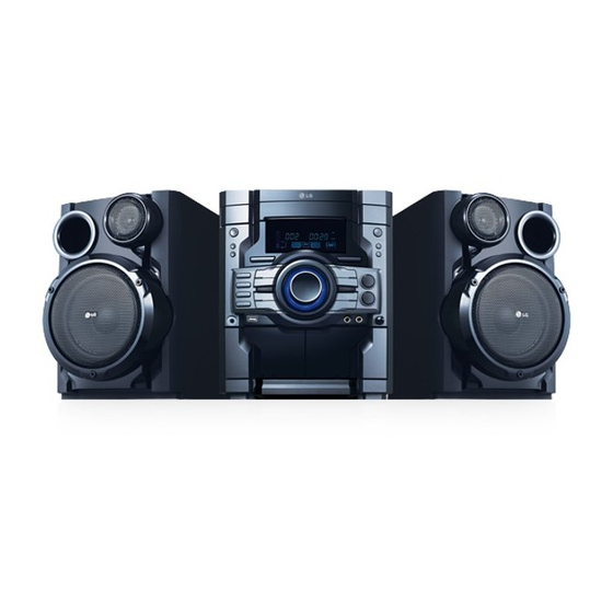
- Page 1 Internal Use Only Website http://biz.lgservice.com DVD Mini Hi-Fi System SERVICE MANUAL CAUTION BEFORE SERVICING THE UNIT, READ THE “SAFETY PRECAUTIONS” IN THIS MANUAL. MODEL : MDD64K (MDS64V) P/NO : AFN73250934 JULY, 2009...
-
Page 2: Table Of Contents
[CONTENTS] SECTION 1. GENERAL • SERVICING PRECAUTIONS ....................1-2 • ESD PRECAUTIONS ......................1-4 • SERVICE INFORMATION FOR EEPROM ................1-5 • PROGRAM DOWNLOAD GUIDE ................... 1-6 • SPECIFICATIONS ......................... 1-7 SECTION 2. EXPLODED VIEWS • CABINET AND MAIN FRAME SECTION ................2-1 •... -
Page 3: Section 1. General
SECTION 1. GENERAL SERVICING PRECAUTIONS NOTES REGARDING HANDLING OF THE PICK-UP 1. Notes for transport and storage 1) The pick-up should always be left in its conductive bag until immediately prior to use. 2) The pick-up should never be subjected to external pressure or impact. Storage in conductive bag Drop impact 2. - Page 4 NOTES REGARDING COMPACT DISC PLAYER REPAIRS 1. Preparations 1) Compact disc players incorporate a great many ICs as well as the pick-up (laser diode). These compo- nents are sensitive to, and easily affected by, static electricity. If such static electricity is high voltage, components can be damaged, and for that reason components should be handled with care.
- Page 5 SAFETY PRECAUTIONS Electrostatically Sensitive Devices (ESD) Some semiconductor (solid state) devices can be damaged easily by static electricity. Such components commonly are called Electrostatically Sensitive Devices (ESD). Examples of typical ESD devices are integrated circuits and some field-effect transistors and semiconductor chip components. The following techniques should be used to help reduce the incidence of component damage caused by static electricity.
-
Page 6: Service Information For Eeprom
SERVICE INFORMATION FOR EEPROM POWER ON FLD no disc status Remote control DETECT NEW EEPROM pause key ->1->4->7->2 in order (OPTION EDIT SCREEN) NAME OPT 0 FLD ‘OP-0…. OPT 1 OPT 2 OPT 3 OPT 4 Move to appropriate position OPT 5 and make changes OPT 6... -
Page 7: Program Download Guide
PROGRAM DOWNLOAD GUIDE Caution) Do not perform any other work such as disconnecting USB device, switching to the Function and turning off the power while downloading it to the set. The USB device should be disconnected after completing the download. •... -
Page 8: Specifications
SPECIFICATIONS General Power supply Refer to main label. Power consumption Refer to main label. Net Weight 5.4 kg External dimensions (W x H x D) 274 x 334 x 344 mm Operating conditions Temperature: 5°C to 35°C, Operation status: Horizontal Operating humidity 5% to 85% Tuner... -
Page 10: Section 2. Exploded Views
SECTION 2. EXPLODED VIEWS 1. CABINET AND MAIN FRAME SECTION (MDD64) NOTES) THE EXCLAMATION POINT WITHIN AN 266A EQUILATERAL TRIANGLE IS INTENDED TO ALERT THE SERVICE PERSONNEL TO THE PRESENCE OF IMPORTANT SAFETY INFORMATION IN SERVICE 266B LITERATURE. 268L 269L 268R 269R MAIN... -
Page 11: Mechanism Exploded View
2. TAPE DECK MECHANISM EXPLODED VIEW (1) TAPE DECK MECHANISM (A/S & A/S : RIGHT A/S DECK) BRASS MOTOR PULLEY MAYBE CHANGED FOR WOW FLUTTER WHEN NECESSARY RING FW MAYBE ADDED FOR WOW FLUTTER WHEN NECESSARY... - Page 12 (2) TAPE DECK MECHANISM (A/S & A/S : LEFT A/S DECK) RING FW MAYBE ADDED FOR WOW FLUTTER WHEN NECESSARY...
- Page 13 3. MECHANISM DECK EXPLODED VIEW (DVM-H1713) 153A 169A 169B 169C...
-
Page 14: Speaker Exploded View
4. SPEAKER EXPLODED VIEW ᆞ FRONT SPEAKER (MDS64V) A60L A62L A60R A62R A61L A61R... -
Page 15: Packing Accessory View
5. PACKING ACCESSORY VIEW 824 AM Loop antenna 801 Instruction Ass'y 825 FM wire antenna 801S Song Book Micro Phone Disc 808 Battery 900 Remote Control 811 RCA Cable, 1Pin(Black) 803 Packing 803 Packing 804 Bag 802 Caja 2-10... -
Page 16: Section 3. Electrical Part
SECTION 3. ELECTRICAL PART AUDIO ELECTRICAL TROUBLESHOOTING GUIDE 1. POWER (SMPS) POWER (SMPS) Check the fuse Replace the fuse F901 Check the DC V of C905 Check BD901, LF901, 902 if DC V is over 400V Check the DC V of C909,C903,C921 Check IC901, 902 Replace IC901,902 If DC V is in 14~19V... - Page 17 3. VKK PART CHECK 2. P-SENS VKK CHECK P-SENS Check Check Check power circuit Check power circuit the pin6 of P9702 the pin3 of P9702 troubleshooting troubleshooting if DC V is over if DC V is over -28V 5.6V 4. MICOM PART CHECK I MICOM PART CHECK I Refer to SMPS...
- Page 18 5. MICOM PART CHECK II MICOM PART CHECK II Refer to SMPS Check P-SENS troubleshooting (P7904_pin6) Check Check both Replace D101 If output of end voltage of D101 D101 is 5V Check If IC103_pin8 and IC100_pin14,40,55,89 are 5V Check D101 X101:32.768KHz X100:9.8304MHz Check the operation...
- Page 19 7. FLD DISPLAY CHECK FLD DISPLAY CHECK Check CN104 pin1, 2, 3 voltage Refer to SMPS troubleshooting input Check if both end voltage of F1,F2 are over 3.4V VKK : over 26V Check CN304 connection and power pin24:FL+26, Check CN304 connection pin23:FL-22, pin22:VKK over 26V, pin19:+5.6V...
- Page 20 8. PWM MODULATION PART CHECK PWM MODULATION PART CHECK Refer to SMPS check P7905 pin9,10 troubleshooting 3.3V Check IC604(PS9830) Check X601 VDD pin voltage (3,10,22,29, Replace X601 12.288MHz 39,47,56,65,72,87,94) check X601 pin2 :3.3V Check X601 12.288MHz operation Check line resistor output check IC604 Replace R671,R670,R665 SDA:R671,SCL:R670...
- Page 21 9. POWER AMP PART CHECK POWER AMP PART CHECK P7905 pin3:+12V Refer to SMPS troubleshooting pin13,14,15:32V Check each IC700 pin27,26,32,35,40,41 input voltage Check each input Check each line resistor output voltage IC700 pin22,23,44:+12V Check PWM modulator input each pin6,8,16,18 POWER output IC700 pin28,31,36,39 Check output Replace the coil line coil...
- Page 22 10. AUX FUNCTION PART CHECK FUNCTION CHECK Each function (tuner/tape/portable) output to IC200(BU4052) input : L/R_CH Check Check IC200 (BU4052) IC200 (BU4052) Check P7905 connection pin3,13 each function pin7:-12V after replace IC200 pin16:+12V output Each function output line check Check Check IC801 IC801 (MC4580) (MC4580)
- Page 23 11. TUNER/TAPE/PORTABLE FUNCTION PART CHECK TAPE PLAY PART CHECK Check IC201 Refer to SMPS troubleshooting (HA12237)_pin16 12V input Check Check A/B Replace head wire and IC201_ pin5,26 DECK head input tape DECK mechanism output signal Check A DECK head input IC201_pin32, 39 and B DECK head input IC201_pin34, 37 Check IC201...
- Page 24 12. TAPE PLAY PART CHECK TAPE REC PART CHECK Check Refer to PWM modulation IC604(PS9830) troubleshooting _pin49, 52 PWM output Check IC201_pin7, 24 record input Check IC201_ Check IC100_ Replace IC201 pin10, 21 output pin23 "HIGH" Check L203_pin2, 3 Check Q205(D1304)_ Check IC202_pin4 "HIGH"...
- Page 25 DVD ELECTRICAL TROUBLESHOOTING GUIDE 1. POWER PART CHECK GUIDE POWER ON POWER ON Does Does Func Check an audio AUX, FM DVD/CD micom or interface 87.5 AM,USB appear at FLD? reconnect (CN201) appear at FLD? Does it appear DVD error at FLD? Check connector Reconnect it (P400)
- Page 26 2. TEST & DEBUG FLOW POWER ON Check connection lines Flash memory between FLASH & ES8390 or Show LOGO? operates properly? the FLASH access time whether is suitable or not Check connection lines SDRAM works between SDRAM (IC502) & properly? ES8390 or the SDRAM is damaged Check the related circuit of...
- Page 27 Does the Motor Driver SLED move to inner side Check the MD DRV_MMUTE pin 3 when it is at outer High position? Check the related circuit of SLED SLED signal is OK? and Motor driver IC (IC401) Do not put in disc Check the cable connection and tray close with MECHA...
- Page 28 Laser turns on Check the laser power circuit DVDLD or CDLD when reading between ES8390 and power output properly? disc? transistor (Q405, Q406) Collector Check the related circuit of voltage of power transistor laser power transistor is ok? (Q405, Q406) Check cable connection between P400 and pick-up head Put disc in tray...
- Page 29 Check the connections between Proper signal on Focus on ok? PDM01 and pick-up head A,B,C,D from MD? Check the related circuit of Proper FOD signal on ES8390 FOCUS signal IC401? Check cable connection between P400 and MD Check the related circuit Proper TRD signal on Tracking ok? between IC401 and ES8390...
- Page 30 Audio outputs are ok Check the connections signal data on during playing between ES8390 and CN201 ES8390 is ok? disk? Check the MAIN PCB For example composite video, Picture Check the video mute TR signal data on TEST END (Q507), ES8390 video signal ES8390 is ok? data 3-15...
- Page 31 3. USB PART TURN ON USB Check "Searching" or Check the POWER supply circuit "USB" Display (Check P201) Check the HRST # signal Check the USB and DVD part Check the USB part supply Check Reading OK (CN205) Check the USB data line (CN205) Check the ES8390 (Check DATA LINE pin98_USB_NO, 99_PO) 3-16...
-
Page 32: Waveforms Of Major Check Point
WAVEFORMS OF MAJOR CHECK POINT 1. WHEN POWER ON, RESET & DATA ETC WAVEFORM SPI DI IC501 pin 72 SPI DO IC501 pin 46 IC501 pin 47 LCS3# (FLASH) IC503 pin 1 HRST# IC501 pin 91 IC501 pin 90 3-17... - Page 33 2. OPEN/CLOSE WAVEFORM AT POWER ON open IC401 pin 11 UP-sw IC501 pin 63 DOWN-sw IC501 pin 59 close IC401 pin 10 3. STARTING ACTION WAVEFORM IN MD DEVICE Driver STBY SLEGN IC401 pin 18 IC401 pin 17 4. FOCUS WAVEFORM (AT CD) IC401 pin 3 IC401 pin 4 3-18...
- Page 34 5. FOCUS WAVEFORM (AT DVD) Q405(DVD_LD) Q405 Q406(CD_LD) Q406 6. AT POWER ON , SPINDLE SIGNAL AT MD DECK Sclavijad IC401 pin 21 Sclavija+ IC401 pin 15 Sclavija- IC401 pin 16 7. TRACKING SIGNAL IC401 pin 7 P400 pin 16 P400 pin 17 3-19...
- Page 35 8. RF WAVEFORM 9. DISK TYPE JUGEMENT WAVEFORM P400 pin 18 IC401 pin 6 SVRRF IC401 pin 23 P400 pin 18 IC401 pin 6 SVRRF IC401 pin 23 3-20...
-
Page 36: Wiring Diagram
WIRING DIAGRAM TUNER MODULE 3-21... -
Page 37: Block Diagrams
BLOCK DIAGRAMS 1. MAIN BLOCK DIAGRAM 3-22... - Page 38 2. DVD BLOCK DIAGRAM SCI,SDA DSCK#,CKE,CS0#,RAS0# DMA[0..11],DB[0..15] SPI_CS,CLK,DI,KO 3-23...
- Page 39 3-24...
-
Page 40: Circuit Diagrams
BE MODIFIED OR ALTERED WITH OUT PERMISSION WAY, IMPLEMENTATION OF THE LATEST SAFETY during Play mode. FROM THE LG CORPORATION. ALL COMPONENTS AND PERFORMANCE IMPROVEMENT CHANGES SHOULD BE REPLACED ONLY WITH TYPES INTO THE SET IS NOT DELAYED UNTIL THE NEW IDENTICAL TO THOSE IN THE ORIGINAL CIRCUIT. - Page 41 2. MPEG CIRCUIT DIAGRAM MPEG EBY57026801_#1 REV4.1 WAVEFORM 2009. 03. 13 3-27 3-28...
- Page 42 3. SERVO CIRCUIT DIAGRAM SERVO EBY57026801_#2 REV4.1 WAVEFORM 2009. 03. 13 3-29 3-30...
- Page 43 4. I/O CIRCUIT DIAGRAM EBY57026801_#3 REV4.1 2009. 03. 13 3-31 3-32...
- Page 44 5. MICOM+INTERFACE CIRCUIT DIAGRAM MICOM+INTERFACE EBY59807101_#1 REV7.1 2009. 03. 13 3-33 3-34...
- Page 45 6. PWM CIRCUIT DIAGRAM EBY59807101_#2 REV7.1 2009. 03. 13 3-35 3-36...
- Page 46 7. AMP CIRCUIT DIAGRAM EBY59807101_#3 REV7.1 2009. 03. 13 3-37 3-38...
- Page 47 8. DECK CIRCUIT DIAGRAM DECK EBY59807101_#4 REV7.1 2009. 03. 13 3-39 3-40...
- Page 48 9. FRONT CIRCUIT DIAGRAM FRONT EBY60660201 REV4.4 2009. 03. 10 3-41 3-42...
- Page 49 10. HEADPHONE CIRCUIT DIAGRAM HEADPHONE EBY60660301 REV5.1 2009. 03. 10 3-43 3-44...
- Page 50 11. MIC CIRCUIT DIAGRAM EBY60660401 REV5.1 2009. 03. 10 3-45 3-46...
- Page 51 12. KEY CIRCUIT DIAGRAM EBY60660501 REV2.2 2009. 03. 10 3-47 3-48...
-
Page 52: Circuit Voltage Chart
CIRCUIT VOLTAGE CHART PIN NO. VOLT PIN NO. VOLT PIN NO. VOLT PIN NO. VOLT PIN NO. VOLT PIN NO. EE Mode (V) EE Mode (V) EE Mode (V) MAIN 1.71 0.002 5.04 1.11 0.59 IC100 (MICOM LC87F5NC8A) 0.001 0.002 5.04 3.35 1.08... - Page 53 EE Mode (V) EE Mode (V) PIN NO. PB Mode (V) PIN NO. EE Mode (V) 0.71 0.01 0.01 1.53 0.91 0.01 3.35 0.71 0.19 3.38 3.47 0.86 1.23 0.94 3.48 1.23 1.38 0.92 1.53 3.38 3.47 0.02 1.79 1.38 2.62 3.26 0.09...
- Page 54 PRINTED CIRCUIT BOARD DIARGAMS 1-1. MAIN P.C. BOARD DIAGRAM ( TOP VIEW ) 3-53 3-54...
- Page 55 1-2. MAIN P.C. BOARD DIAGRAM ( BOTTOM VIEW ) 3-55 3-56...
- Page 56 2-1. DVD P.C. BOARD DIAGRAM ( TOP VIEW ) 3-57 3-58...
- Page 57 2-2. DVD P.C. BOARD DIAGRAM ( BOTTOM VIEW ) 3-59 3-60...
- Page 58 3. SMPS P.C. BOARD DIAGRAM NOTE: Warning Parts that are shaded are critical With respect to risk of fire or electrical shock. 3-61 3-62...
- Page 59 4. FRONT P.C. BOARD DIAGRAM 5. HEADPHONE P.C. BOARD DIAGRAM 6. KEY P.C. BOARD DIAGRAM (OPTIONAL PART) 7. MIC P.C. BOARD DIAGRAM 3-63 3-64...