
Related Manuals for Sony CVX-V1


Summary of Contents for Sony CVX-V1
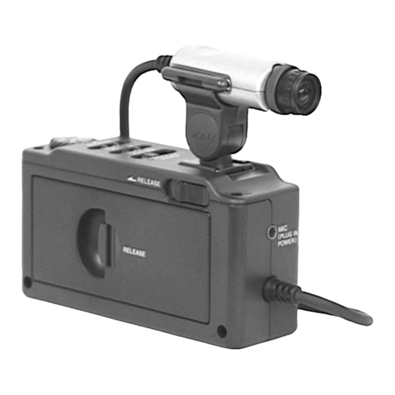
- Page 1 CVX-V1/V1P SERVICE MANUAL US Model Canadian Model CVX-V1 AEP Model UK Model CVX-V1P Photo: CVX-V1P NTSC model: CVX-V1 PAL model : CVX-V1P SPECIFICATIONS COLOR VIDEO CAMERA MICROFILM...
- Page 2 SONY PARTS WHOSE PART NUMBERS APPEAR AS DE FONCTIONNEMENT. NE REMPLACER CES COM- SHOWN IN THIS MANUAL OR IN SUPPLEMENTS PUB- POSANTS QUE PAR DES PIÈCES SONY DONT LES LISHED BY SONY. NUMÉROS SONT DONNÉS DANS CE MANUEL OU DANS LES SUPPLÉMENTS PUBLIÉS PAR SONY.
-
Page 3: Table Of Contents
TABLE OF CONTENTS Section Title Page Section Title Page GENERAL 1-3. Camera System Adjustments ........5-9 ..............1-1 1. 28 MHz Origin Oscillation Adjustment ..... 5-9 2. Picture Frame Setting ..........5-10 3. Color Reproduction Adjustment ....... 5-11 DISASSEMBLY 4. Auto White Balance Reference Data Input ....5-12 5. -
Page 4: General
CVX-V1/V1P SECTION 1 GENERAL... - Page 5 1-2 E...
-
Page 6: Disassembly
CVX-V1/V1P SECTION 2 DISASSEMBLY Note: Follow the disassembly procedure in the numerical order given. 2-1. REMOVAL OF CABINET (LOWER) 2-3. REMOVAL OF CAMERA HEAD ASSEMBLY ASSEMBLY, CS-53 BOARD 2 Camera head assembly 1 Two tapping screws 3 Claw 9 Tapping screw... -
Page 7: Removal Of Lens (Ccd) Assembly
2-4. REMOVAL OF LENS (CCD) ASSEMBLY 2 Two screws (P2) Note 1: When remove a connector, don't pull at 3 Cabinet wire of connector. (upper) Be in danger of the snapping of a wire. 5 Screw (M1.7 × 3) 6 Two connectors (CN101, 102) (Note1, 2) 7 Connection cord... -
Page 8: Block Diagrams
CVX-V1/V1P CVX-V1/V1P SECTION 3 BLOCK DIAGRAMS 3-1. OVERALL BLOCK DIAGRAM LENS BLOCK CD-188 BOARD CS-53 BOARD VA-103 BOARD (SEE PAGE 4-7 - 4-9) (SEE PAGE 4-15 - 4-24) (SEE PAGE 4-33 - 4-41E) IC307 IC701 J701 CAMERA IC305 CAM Y... -
Page 9: Camera (1) Block Diagram
3.2V 17.734475MHz CAMERA/MODE CONTROL TG SCK 3Vp-p OSC I XSHT Q503 CVX-V1P CN101 MUTE CAMERA BLOCK 2 V=60 Hz: CVX-V1 CAM VD MUTE I MUTE XSGI V=50 Hz: CVX-V1P VA-103 BOARD –7.0V IC307 CN801 IC309 2.3 Vp-p (SEE PAGE 3-9) -
Page 10: Camera (2) Block Diagram
CVX-V1/V1P 3-3. CAMERA (2) BLOCK DIAGRAM 3-4. AUDIO BLOCK DIAGRAM CS-53 BOARD VA-103 BOARD VA-103 BOARD 1.1 Vp-p 1.8 Vp-p (SEE PAGE 4-21,4-23) (SEE PAGE 4-37) (SEE PAGE 4-33 - 4-41E) 0.46 Vp-p IC701 IC701 IC701 IC401 MIC AMP IC701... -
Page 11: Power Block Diagram
CVX-V1/V1P 3-5. POWER BLOCK DIAGRAM (FOR CHECK) IF-69 BOARD VA-103 BOARD CN805 (SEE PAGE 4-41E) (SEE PAGE 4-33 - 4-41E) LANC DC CN802 CN901 CN902 UNREG UNREG L901 EASY BATTERY IC801 LANC I/O CONNECTOR TERMINAL CN601 F601 BATT (+) UNREG... -
Page 12: Frame Schematic Diagram
CVX-V1/V1P SECTION 4 PRINTED WIRING BOARDS AND SCHEMATIC DIAGRAMS 4-1. FRAME SCHEMATIC DIAGRAM FRAME... -
Page 13: Cd-188 (Ccd Imager), (Timing Generator) Schematic Diagrams
CVX-V1/V1P CD-188 (CCD IMAGER), (TIMING GENERATOR) SCHEMATIC DIAGRAM CD-188 BOARD (2/2) 7 Vp-p IC101 @∞, @§ 7 Vp-p IC101 @•, #¡ 3 Vp-p IC101 $¢ 3 Vp-p IC101 $∞ CD-188 BOARD (1/2) Precautions for Replacement of CCD Imager • The CD-188 board mounted as a repair part is not equipped with a CCD imager. - Page 14 CVX-V1/V1P CS-53 (CAMERA, Y/C PROCESS, MIC AMP, MODE CONTROL) PRINTED WIRING BOARD – Ref. No.: CS-53 board; 1,000 series – • For printed wiring board. There are few cases that the part isn't mounted in this model is printed on this diagram.
-
Page 15: Camera, Y/C Process) Schematic Diagram
0.9 Vp-p 14.318 MHz: NTSC 14.187 MHz: PAL IC305 !§ IC307 @£ 2.3 Vp-p 3.2 Vp-p 17.734475 MHz 0.14usec IC307 ^£ IC305 2 – 0 NTSC model: CVX-V1 PAL model : CVX-V1P CAMERA, Y/C PROCESS CS-53 (1/3) 4-15 4-16 4-17 4-18... -
Page 16: Mode Control) Schematic Diagram
CS-53 (MODE CONTROL) SCHEMATIC DIAGRAM • See page 4-11 for CS-53 BOARD printed wiring board. CS-53 BOARD (2/3) 3 Vp-p V=60Hz: NTSC V=50Hz: PAL IC502 ^™ 0.7 Vp-p 32.768 kHz IC502 %™ 0.2 Vp-p 20 MHz IC502 $¡ NTSC model: CVX-V1 PAL model : CVX-V1P MODE CONTROL CS-53 (2/3) 4-20 4-21 4-22... -
Page 17: Mic Amp) Schematic Diagram
CVX-V1/V1P CVX-V1/V1P CS-53 (MIC AMP) SCHEMATIC DIAGRAM • See page 4-11 for CS-53 BOARD printed wiring board. MIC AMP CS-53 (3/3) 4-23 4-24... - Page 18 CVX-V1/V1P • For printed wiring boards. There are few cases that the part isn't mounted in this model is printed on this diagram. • VA-103 board is 4-layers print board. However, the patterns of VA-103 (DC-DC CONVERTER, VIDEO/AUDIO I/O, LANC I/O), IF-69 (INTERFACE) PRINTED WIRING BOARDS layers 2 to 3 have not been included in the diagram.
-
Page 19: Va-103 (Dc-Dc Converter, Video/Audio I/O, Lanc I/O)
CVX-V1/V1P VA-103 (DC-DC CONVERTER) SCHEMATIC DIAGRAM VA-103 BOARD (1/3) 13 Vp-p 2.0 µsec Q601 C DC-DC CONVERTER VA-103 (1/3) 4-33 4-34 4-35... -
Page 20: Va-103 (Video/Audio I/O) Schematic Diagram
CVX-V1/V1P VA-103 (VIDEO/AUDIO I/O) SCHEMATIC DIAGRAM • See page 4-28 for VA-103 BOARD printed wiring board. VA-103 BOARD (2/3) 0.46 Vp-p IC701 @™ 0.5 Vp-p IC701 !§ 1.0 Vp-p IC701 !¢ 1.8 Vp-p IC701 9 2.1 Vp-p IC701 6 1.1 Vp-p IC701 #¡... -
Page 21: Va-103 (Lanc I/O), If-69 (Interface) Schematic Diagrams
CVX-V1/V1P VA-103 (LANC I/O), IF-69 (INTERFACE) SCHEMATIC DIAGRAM • See page 4-28 for VA-103 BOARD and IF-69 BOARD printed wiring boards. LANC I/O INTERFACE VA-103 (3/3) IF-69 4-39 4-40 4-41 E... -
Page 22: Adjustments
CVX-V1/V1P SECTION 5 ADJUSTMENTS 5-1. CAMERA SECTION ADJUSTMENT NTSC model: CVX-V1 PAL model : CVX-V1P 1-1. PREPARATIONS BEFORE ADJUSTMENT 1-1-1. List of Service Tools • Oscilloscope • Regulated power supply • Vectorscope • Frequency counter • Color monitor • Digital voltmeter Ref. -
Page 23: Preparations
1-1-2. Preparations Note 1: For details of how remove the cabinet and boards, refer Pattern box to “2. DISASSEMBLY”. 1) Connect the equipment for adjustments according to Fig. 5-1-3. 2) Connect the adjustment remote commander to the CN805 on the VA-103 board via CPC-5 (J-6082-351-A). Front side of the lens L = About 40 cm Fig. -
Page 24: Precaution
1-1-3. Precaution 1. Setting the Switch Unless otherwise specified, set the switches as follows and per- form adjustments. 1. POWER switch (Control switch block) ....ON 2. AE LOCK switch (Control switch block) ... OFF 2. Order of Adjustments Basically carry out adjustments in the order given. Electronic beam scanning frame 0 ±... -
Page 25: Adjustment Remote Commander
1-1-4. ADJUSTMENT REMOTE COMMANDER 2. Precautions Upon Using The adjustment remote commander is used for changing the cal- The Adjustment Remote Commander culation coefficient in signal processing, EVR data, etc. The ad- Mishandling of the adjustment remote commander may erase the justment remote commander performs bi-directional communica- correct adjustment data at times. -
Page 26: Data Process
1-1-5. DATA PROCESS The calculation of the DDS display and the adjustment remote commander display data (hexadecimal notation) are required for obtaining the adjustment data of some adjustment items. In this case, after converting the hexadecimal notation to decimal nota- tion, calculate and convert the result to hexadecimal notation, and use it as the adjustment data. -
Page 27: Initialization Of F
1-2. INITIALIZATION OF F PAGE DATA 3. F Page Table Note: Fixed data-1 : Initialized data. ( Refer to “1. Initializing 1. Initializing the F Page Data the F Page Data”.) Note: If the F page data has been initialized, “Modification of F Fixed data-2 : Modified data. - Page 28 Address Initial Remark Address Initial Remark value value NTSC PAL NTSC PAL Auto White Balance Fixed data1 3D Reference Data Input (Initialized data) Fixed data1 Picture Frame Setting Fixed data1 (Initialized data) Fixed data2 Fixed data1 28MHz Origin Oscillation Adj. Fixed data1 (Initialized data) Fixed data2...
- Page 29 Address Initial Remark Address Initial Remark value value NTSC PAL NTSC PAL Fixed data2 Fixed data1 (Initialized data) Fixed data1 (Initialized data) FE Color Reproduction Adj. Fixed data2 Fixed data1 (Initialized data) Fixed data2 Fixed data1 (Initialized data) Fixed data2 Fixed data1 (Initialized data) Fixed data2...
-
Page 30: Camera System Adjustments
1-3. CAMERA SYSTEM ADJUSTMENTS 1. 28 MHz Origin Oscillation Adjustment (CS-53 board) Set the frequency of the clock for synchronization. If deviated, the synchronization will be disrupted and the color will become in- consistent. Subject Not required Pin !™ of IC304 Measurement Point Measuring Instrument Frequency counter... -
Page 31: Picture Frame Setting
2. Picture Frame Setting Check on the oscilloscope Color bar chart standard picture frame Subject 1. Horizontal period (40 cm from the front of the lens) Measurement Point Video output terminal Measuring Instrument Oscilloscope and TV monitor Adjustment page Adjustment address 36, 37 Specified Value A = B, C = D, t = 0 ±... -
Page 32: Color Reproduction Adjustment
3. Color Reproduction Adjustment For NTSC model Adjust the color Separation matrix coefficient so that proper color reproduction is produced. Color bar chart standard picture Subject frame Measurement Point Video output terminal Measuring Instrument Vectorscope Adjustment Page Adjustment Address 44, 46, AA, AB Specified Value All color luminance points should settle within each color reproduc-... -
Page 33: Auto White Balance Reference Data Input
4. Auto White Balance Reference Data Input 5. Auto White Balance Adjustment Adjust to the proper auto white balance output data. Clear chart Subject If it is not correct, auto white balance and color reproducibility (Color bar standard picture frame) will be poor. -
Page 34: White Balance Check
6. White Balance Check Clear chart Subject (Color bar standard picture frame) Filter C14 for color temperature Filter correction ND filter 1.0 and 0.3 Measurement Point Video output terminal Measuring Instrument Vectorscope Specified Value Fig. 5-1-10. (A) to (C) Checking method: Fig. -
Page 35: Battery Down Adjustment
7. Battery Down Adjustment 11) Select page: F, address: 5B, set data: X , and press the PAUSE Set the battery end voltage. button of the adjustment remote commander. 12) Select page: F, address: 5C, set data: X , and press the PAUSE Mode Camera on button of the adjustment remote commander. -
Page 36: Repair Parts List
X-3949-037-1 CABINET (LOWER) ASSY (CVX-V1P) * 33 3-704-367-01 LABEL (CVX-V1) 3-989-177-01 SHOE * 34 3-704-437-01 LABEL, CAUTION, FUSE REPLACEMENT 3-989-178-01 SPRING, SHOE LEAF (CVX-V1) 1-783-521-22 CORD, CONNECTION IC001 8-752-616-03 IC ICX208AK-43 (CCD IMAGER) (CVX-V1) IC001 8-752-616-11 IC ICX209AK-43 (CCD IMAGER) (CVX-V1P) -
Page 37: Electrical Parts List
1-218-973-11 RES,CHIP 1/16W C003 1-164-943-11 CERAMIC CHIP 0.01uF C004 1-109-982-11 CERAMIC CHIP C005 1-164-844-11 CERAMIC CHIP 0.25PF 16V A-7073-696-A CS-53 BOARD, COMPLETE (CVX-V1) C006 1-109-982-11 CERAMIC CHIP ****************************** A-7073-693-A CS-53 BOARD, COMPLETE (CVX-V1P) C101 1-135-259-11 TANTAL. CHIP 10uF 6.3V *******************************... - Page 38 CS-53 Ref. No. Part No. Description Remark Ref. No. Part No. Description Remark C334 1-162-917-11 CERAMIC CHIP 15PF FB313 1-414-228-11 INDUCTOR CHIP 0UH (CVX-V1P) FB314 1-500-284-21 INDUCTOR CHIP 0UH C335 1-107-826-11 CERAMIC CHIP 0.1uF FB315 1-414-228-11 INDUCTOR CHIP 0UH C336 1-162-970-11 CERAMIC CHIP 0.01uF FB316...
- Page 39 < VIBRATOR > R334 1-216-823-11 METAL CHIP 1.5K 1/16W R335 1-216-829-11 METAL CHIP 4.7K 1/16W X301 1-760-320-11 VIBRATOR, CRYSTAL (28.636MHz) (CVX-V1) (CVX-V1P) X301 1-760-321-11 VIBRATOR, CRYSTAL (28.375MHz) (CVX-V1P) R338 1-216-821-11 METAL CHIP 1/16W X302 1-579-613-11 VIBRATOR, CRYSTAL (17.734475MHz) (CVX-V1P) R339 1-216-827-11 METAL CHIP 3.3K...
- Page 40 Remark A-7073-692-A VA-103 BOARD, COMPLETE (CVX-V1P) C733 1-107-826-11 CERAMIC CHIP 0.1uF C734 1-110-569-11 TANTAL. CHIP 47uF 6.3V ******************************* A-7073-695-A VA-103 BOARD, COMPLETE (CVX-V1) C735 1-162-920-11 CERAMIC CHIP 27PF C736 1-162-920-11 CERAMIC CHIP 27PF ****************************** (Ref.No.:1,000 Series) C737 1-162-970-11 CERAMIC CHIP 0.01uF...
- Page 41 1-414-754-11 INDUCTOR 10uH R704 1-216-821-11 METAL CHIP 1/16W L702 1-414-757-11 INDUCTOR 100uH R705 1-216-821-11 METAL CHIP 1/16W L703 1-412-798-11 INDUCTOR 68uH (CVX-V1) L703 1-412-796-41 INDUCTOR 47uH (CVX-V1P) R706 1-216-821-11 METAL CHIP 1/16W R707 1-216-821-11 METAL CHIP 1/16W < LINE FILTER >...
- Page 42 1-783-522-11 CABLE, FLEXIBLE FLAT (FFC-246) 1-783-523-11 CABLE, FLEXIBLE FLAT (FFC-247) 1-475-734-11 SWITCH BLOCK, CONTROL (VC) 1-758-186-11 LENS, VIDEO (VCL-3901VB) 1-758-157-11 FILTER BLOCK, OPTICAL IC001 8-752-616-03 IC ICX208AK-43 (CCD IMAGER) (CVX-V1) IC001 8-752-616-11 IC ICX209AK-43 (CCD IMAGER) (CVX-V1P) ACCESSORIES ************ 1-784-838-21 ADAPTOR, CONNECTION...
- Page 43 FOR CAMERA COLOR REPRODUCTION ADJUSTMENT Take a copy of CAMERA COLOR For NTSC model REPRODUCTION FRAME and Parts reference sheets with a clear sheet for use. CVX-V1 For PAL model CVX-V1P...
- Page 44 You can find the parts position of mount locations applying to VA-103 board of a set. S I D E B CN801 VA-103 BOARD I C 6 0 1 CN802 CN601 IC702 CN803 I C 6 0 2 CN804 I C 8 0 1 SIDE A CVX-V1/ V1P...
- Page 45 CVX-V1/V1P Sony Corporation 98H0512-1 Printed in Japan © 1998. 8 9-974-102-11 Personal A&V Products Company Published by Quality Assurance Dept. – 92 – (Osaki East)