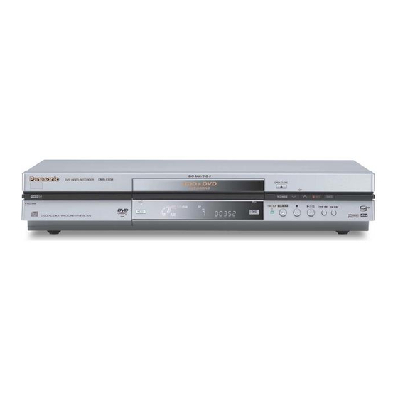
Panasonic DMR-E80HP Service Manual
Dvd video recorder
Hide thumbs
Also See for DMR-E80HP:
- Operating instructions manual (64 pages) ,
- Servise manual (33 pages)
Table of Contents
Advertisement
Quick Links
SPECIFICATIONS
Power supply:
Power consumption:
Recording system:
Optical pick-up:
Recordable discs:
Recording time:
(Using 4.7 GB disc):
ORDER NO.DSD0306005C1
DMR-E80HP / DMR-E80HPC
(S).......................Silver Type
Specifications
AC120 V, 60 Hz
35 W
DVD video recording
standards (DVD-RAM),
DVD video standards (DVD-
R)
System with 1 lens, 2
integration units (662 nm
wavelength for DVDs, 790
nm wavelength for CDs)
12 cm 4.7 GB DVD-RAM
discs
12 cm 9.4 GB DVD-RAM
discs
8 cm 2.8 GB DVD-RAM discs
12 cm 4.7 GB DVD-R discs
(for General Ver. 2.0)
8 cm 1.4 GB DVD-R discs
(for General Ver. 2.0)
Max. 6 hours
XP: 60 minutes
SP: 120 minutes
LP: 240 minutes
EP: 360 minutes
1
DVD Video Recorder
Colour
B24
Advertisement
Table of Contents

Related Manuals for Panasonic DMR-E80HP


Summary of Contents for Panasonic DMR-E80HP
- Page 1 ORDER NO.DSD0306005C1 DVD Video Recorder DMR-E80HP / DMR-E80HPC Colour (S).......Silver Type SPECIFICATIONS Specifications Power supply: AC120 V, 60 Hz Power consumption: 35 W Recording system: DVD video recording standards (DVD-RAM), DVD video standards (DVD- Optical pick-up: System with 1 lens, 2...
-
Page 2: Dvd-Videodiscs
(Using built-in HDD): Max. 104 hours XP: 17 hours SP: 34 hours LP: 68 hours EP: 104 hours (continuous recording time is 6 hours max.) Region number: Region No.1 Discs played: 12 cm 4.7 GB DVD-RAM discs 12 cm 9.4 GB DVD-RAM discs 8 cm 2.8 GB DVD-RAM discs 12 cm 4.7 GB DVD-R discs... - Page 3 Input: LINE (pin jack) Reference input: 309 mVrms FS: 2 Vrms (1 kHz, 0 dB) Input impedance: 47 k Output: LINE (pin jack) Reference output: 309 mVrms FS: 2 Vrms (1 kHz, 0 dB) Output impedance: 1 k (Load impedance: 10 k Number of channels: Recording: 2 channels Playback: 2 channels...
-
Page 4: Safety Precautions
1. SAFETY PRECAUTIONS 1.1. GENERAL GUIDELINES 1. When servicing, observe the original lead dress. If a short circuit is found, replace all parts which have been overheated or damaged by the short circuit. 2. After servicing, see to it that all the protective devices such as insulation barriers, insulation papers shields are properly installed. -
Page 5: Prevention Of Electro Static Discharge
3. Use an AC voltmeter, with 1000 ohms/volt or more sensitivity, to measure the potential across the resistor. 4. Check each exposed metallic part, and measure the voltage at each point. 5. Reverse the AC plug in the AC outlet and repeat each of the above measurements. -
Page 6: Precaution Of Laser Diode
removal devices not classified as "anti-static (ESD protected)" can generate electrical charge sufficient to damage ES devices. 5. Do not use freon-propelled chemicals. These can generate electrical charges sufficient to damage ES devices. 6. Do not remove a replacement ES device from its protective package until immediately before you are ready to install it. -
Page 7: How To Replace The Lithium Battery
( As shown in 15.2.1. The Main P.C.B. ) NOTE: The lithium battery is a critical component. ( Type No.: CR2032-1GUF Manufactured by Panasonic. ) It must never be subjected to excessive heat or discharge. It must therefore only be fitted in equipment designed specifically for its use. -
Page 8: Handling The Lead-Free Solder
5. Handling the Lead-free Solder 5.1. About lead free solder (PbF) Distinction of PbF P.C.B.: P.C.B.s (manufactured) using lead free solder will have a PbF stamp on the P.C.B. Caution: - Pb free solder has a higher melting point than standard solder; Typically the melting point is 50 - 70°F (30 - 40°C) higher. - Page 9 STOP, and OPEN / CLOSE simultaneously for five seconds. - Process mode 1 setting: While the power is off, press SKIP(R), TIME SLIP, and OPEN / CLOSE simultaneously for five seconds. 2. For disassembly and replacement procedures, refer to the “Assembling and Disassemling”.
- Page 10 6.2. Service Explorer in Detail 6.2.1. Does not operate items needed: RAM drive, digital P.C.B., remote control. Conditions: Nothing special.
- Page 11 6.2.2. Poor Pictures Items needed: RAM drive, Digital P.C.B., RF cable, AV cable. Conditions: Check with TU IN-AV OUT(EE). When recording or playback is partially needed, follow the instructions.
- Page 12 6.2.3. Other Items needed: Digital P.C.B., HDD. Conditions: Nothing special.
- Page 13 6.2.4. Caution when replacing the parts 1. RAM Drive In case the unit does not operate normally after replacement of the RAM Drive with new one. A. While power is off, press [SKIP], [TIME SLIP] and [OPEN/ CLOSE] keys simultaneously for five seconds. Then the unit turns into “TEST Mode”, and the region code is stored on the new RAM Drive automatically.
-
Page 14: Standard Inspection Specifications After Making Repairs
Procedure Item to Check Turn on the power. The Panasonic RAM disc should be recognized. Enter the EE (TU IN / AV IN - AV OUT) mode. No abnormality should be seen in the picture, sound or operation. Perform auto recording and playback for one No abnormality should be seen in the picture, minute using the RAM disc. -
Page 15: Assembling And Disassembling
Item Contents Item Contents Check Block noise Distorted sound Crosscut noise noise (static, background noise, etc.) Dot noise The sound level is too low. Picture Picture disruption Sound The sound level is too high. Not bright enough The sound level changes. Too bright Flickering color Color fading... - Page 16 8.2. P.C.B. Positions 8.3. The Top Cover 1. Remove the 2 screws (A) and 3 screws (B). 2. Open the both ends at the front side of the Top cover a bit and lift the Top cover in the direction of the arrows.
- Page 17 8.4. The Front panel 1. Remove the 2 connectors. 2. Remove the 2 tabs (A) and 3 tabs (B) in this order. (The tab (A) and the tab (B) should be removed at the same time, respectively.) 3. Move the front panel to your side slowly and remove it.
- Page 18 8.5. The Front (L) and (R) P.C.B. 1. Remove the 2 screws and remove the Front Angle. 2. Remove the 4 screws (A) and remove the Front (R) P.C.B. 3. Remove the 2 screws (B) with Earth plate and remove the Front (L) P.C.B.
-
Page 19: The Atapi P.c.b
8.6.1. In case of removing Fan motor from Rear panel 1. Remove the 2 screws. 2. Remove the 2 tabs. 8.7. The ATAPI P.C.B. 1. Remove a screw. 2. Remove the connector. 1. Remove the FFC. CAUTION: When replacing ATAPI P.C.B., pay attention as below. - Page 20 8.8. The Digital P.C.B. 1. Remove the FFC(A) and FFC(B).. CAUTION: When replacing Digital P.C.B., pay attention as below. 2. Remove the 2 screws. 3. Press each tab with the nipper to pull out the 3 Connectors and Digital P.C.B.
- Page 21 8.9. HDD 1. Remove the 4 screws. 2. Pull out the HDD holder vertically from Super sheet and HDD...
-
Page 22: The Dvd-Ram Drive
Handling of HDD The following precautions should be taken when handling HDD. 1. Never give an impact to HDD. (Even a drop from 1cm height can be a cause of HDD failure.) 2. When placing HDD on a workbench, provide a mat on a bench for shock absorption and anti-static purposes. - Page 23 8.11. The Main Power Supply P.C.B. and Main P.C.B. 1. Remove the 4 screws (A). 2. Remove the HDD bracket. 3. Remove the 2 connectors and 2 tabs (A). 4. Remove the Main Power Supply P.C.B and tab (B) , pull out it in the direction of the arrow.
-
Page 24: Service Positions
9. Service Positions 9.1. Checking procedure Note: For the disassembling procedure, see the section 8. 9.2. Checking the Digital P.C.B. 1. Remove the Top Cover. 2. Remove the FFC (ATAPI - Digital P.C.B.). 3. Remove the FFC (RAM Drive - Digital P.C.B.) 4. - Page 25 9.3. Checking the Main P.C.B. 1. Remove the Top Cover. 2. Remove the Front Panel. 3. Remove the Rear Panel. 4. Remove the Power Supply P.C.B., Main P.C.B. and RAM Drive and HDD. 5. Use the extension cable (RFKZ0168) to connect the Main P.C.B. and Fan Motor.
- Page 26 P.C.B. and Front P.C.B. (R). Service tools Extension Cable RFKZ0165 (20Pin) (Main P.C.B. - Front (L) P.C.B.) Extension Cable RFKZ0166 (10Pin) (Power supply P.C.B. - Front (R) P.C.B.) Extension Cable RFKZ0169 (4Pin) (HDD - Power supply P.C.B.) Extension cable RFKZ0168 (3Pin) (Fan motor) 9.4.
- Page 27 Power supply P.C.B. 6. Remove the Power Supply P.C.B., fix it on the insulation sheet. 7. Use the extension cables (RFKZ0170,RFKZ0171) to connect the Main P.C.B. and Power Supply P.C.B.. 8. Use the extension cable (RFKZ0165) to connect the Main P.C.B. and Front (L) P.C.B.
-
Page 28: Video Plus
10. List of Various Mode 10.1. List of Various Buttons Each buttons Functions name To turn power on or off on the DVD. VIDEO Plus+ To set timer program using G (Show View/G code/Show view/VIDEO Plus+ code) To set AV input on the TV. Numeric To put each number for buttons(10key) -
Page 29: Play List/Menu
Each buttons Functions name CH UP/DOWN To select channel on the TV or DVD. VOLUME UP/ To control volume on the TV. DOWN SLOW/SEARCH <SLOW> To set the slow mode during still. <SEARCH> To set the cue or review during playback. PLAY/X1.3 <PLAY>... - Page 30 Each buttons Functions name FRAME (Reverse/ To set frame advance. Forward) POSITION To memorize STOP position for MEMORY playing back again. * STOP position is erased by turning power off and openning tray. MARKER (DVD-RAM/-R)To put marker for making chapter. AV LINK To playback on the DVD and select AV1 mode on the TV...
- Page 31 Item FL display Key operation Mode name Description Remote controller key Clear item Items 1-20 are cleared. [0] [0] while in service mode Error code display FL display of the last [0] [1] while in service mode error code held by timer ROM version display Region code, main, [0] [2] while in service mode...
- Page 32 Item FL display Key operation Mode name Description Remote controller key RTSC return XP (A& Disc recording of L1 Initialization mode (EE2/ [1] [3] while in service mode input Encoded and Interlace/ XP/ Audio decoded for external 48kHz) output without playback.
- Page 33 Item FL display Key operation Mode name Description Remote controller key Audio pattern output The audio pattern Initialization mode [2] [3] while in service mode stored in the internal (Interlace) memory is output (1kHz-18dB). Audio 44.1kHz / 48kHz [2] [4] while in white picture switched.
- Page 34 Item FL display Key operation Mode name Description Remote controller key Factors which The disc condition is [4] [4] while in service mode cause drive error displayed when an error occures. Disc manufacture ID Display the [4] [5] while in service mode manufacture’s ID for a disc on which a drive error has occured.
-
Page 35: Test Mode
Item FL display Key operation Mode name Description Remote controller key Main unit All parameters [9] [9] while in service mode initialization (including timer) are initiaized to the factory setting. 10.2.2. Other special modes Item FL display Key operation Mode name Description Remote controller key TEST Mode... - Page 36 10.2.3. List of the U/H/F Error Displays Diagnosis Description FL display Display Remote control Display appears when main unit and remote mode error controller modes are not matched. Abnormal inner Display appears when the drive temperature temperature exceeds 71Åé. Main unit is powered off detected forcibly.
- Page 37 Diagnosis Description FL display Display Drive hardware Display appears when drive unit error is error detected. The event is saved in memory. Remains displayed. Initialization error Display appears when initialization error is when main detected after starting up main microprocessor microprocessor for program recording.
- Page 38 10.3.2. Error generating disk state 10.3.3. Disk production maker ID * Since a display is arbitrarily set up by the disk producer side, the above-mentioned display may be changed. Please make it reference as an example of a display. 11. Abbreviations...
- Page 39 INITIAL/LOGO ABBREVIATIONS A0~UP ADDRESS ACLK AUDIO CLOCK AD0~UP ADDRESS BUS ADATA AUDIO PES PACKET DATA ADDRESS LATCH ENABLE AMUTE AUDIO MUTE AREQ AUDIO PES PACKET REQUEST AUDIO RF SERVO AMP INVERTED INPUT SERVO AMPOUTPUT ASYNC AUDIO WORD DISTINCTION SYNC BIT CLOCK (PCM) BCKIN BIT CLOCK INPUT BLACK DROP OUT...
- Page 40 INITIAL/LOGO ABBREVIATIONS DACCK D/A CONVERTER CLOCK DEEMP DEEMPHASIS BIT ON/OFF DEMPH DEEMPHASIS SWITCHING DIG0~UP FL DIGIT OUTPUT DATA INPUT DMSRCK DM SERIAL DATA READ CLOCK DMUTE DIGITAL MUTE CONTROL DROP OUT DOUT0~UP DATAOUTPUT DATA SLICE RF (BIAS) DRPOUT DROP OUT SIGNAL DREQ DATA REQUEST DRESP...
- Page 41 INITIAL/LOGO ABBREVIATIONS IECOUT IEC958 FORMAT DATA OUTPUT IPFRAG INTERPOLATION FLAG IREF I (CURRENT) REFERENCE ISEL INTERFACE MODE SELECT LDON LASER DIODE CONTROL LASER POWER CONTROL LRCK L CH/R CH DISTINCTION CLOCK MA0~UP MEMORY ADDRESS MEMORY CLOCK MCKI MEMORY CLOCK INPUT MCLK MEMORY SERIAL COMMAND CLOCK...
- Page 42 INITIAL/LOGO ABBREVIATIONS READ ENABLE RFENV RF ENVELOPE RF PHASE DIFFERENCE OUTPUT (CD-ROM) REGISTER SELECT RSEL RF POLARITY SELECT RESET RESERVE SBI0, 1 SERIAL DATA INPUT SBO0 SERIAL DATA OUTPUT SBT0, 1 SERIAL CLOCK SERIAL DATA CLOCK SCKR AUDIO SERIAL CLOCK RECEIVER SERIAL CLOCK SCLK...
- Page 43 SYSTEM CLOCK INITIAL/LOGO ABBREVIATIONS TRACKING ERROR TIBAL BALANCE CONTROL BALANCE OUTPUT 1 BALANCE INPUT BALANCE INPUT BALANCE OUTPUT 2 TPSN OP AMP INPUT TPSO OP AMP OUTPUT TPSP OP AMP INVERTED INPUT TRCRS TRACK CROSSSIGNAL TRON TRACKING ON TRSON TRAVERSE SERVO ON INITIAL/LOGO ABBREVIATIONS VBLANK...
-
Page 44: Voltage And Waveform Chart
INITIAL/LOGO ABBREVIATIONS X' TAL XALE X ADDRESS LATCH ENABLE XAREQ X AUDIO DATA REQUEST XCDROM X CD ROM CHIP SELECT X CHIP SELECT XCSYNC X COMPOSITE SYNC X DATA STROBE XHSYNCO X HORIZONTAL SYNC OUTPUT XHINT XH INTERRUPTREQUEST X' TAL OSCILLATOR INPUT XINT X INTERRUPT X MEMORY WRITE ENABLE... -
Page 45: Block Diagram
13. Block Diagram 13.1. Power Supply Block Diagram 13.1.1. Integrated Circuit Power Supply Chart ( PSC 1 - PSC 15 ) 13.2. Analog Video Block Diagram 13.3. Analog Audio Block Diagram 13.4. Timer Block Diagram 13.5. Digital Section Block Diagram 13.5.1. -
Page 46: Print Circuit Board
14.15. Front (L) Schematic Diagram 14.16. Front (R) Schematic Diagram 15. Print Circuit Board 15.1. Main Power Supply P.C.B. 15.2. Main P.C.B. 15.2.1. Main P.C.B. ( Section 1/4 ) 15.2.2. Main P.C.B. ( Section 2/4 ) 15.2.3. Main P.C.B. ( Section 3/4 ) 15.2.4. - Page 47 16.2. Casing Parts & Mechanism Section 2...
- Page 48 16.3. Packing & Accessories Section...
-
Page 49: Replacement Parts List
17. Replacement Parts List Notes: *Important safety notice: Components identified by mark have special characteristics important for safety. Furthermore, special parts which have purposes of fire-retardant (resistors), high-quality sound (capacitors), low-noise (resistors), etc. are used. When replacing any of components, be sure to use only manufactures specified parts shown in the parts list. - Page 50 FRONT ORNAMENT(R) 20-11 RGK1622-K FRONT ORNAMENT(L) 20-12 RKF0667-K TRAY DOOR 20-13 VMB3410 BLINDER SPRING 20-14 XTN2+6G SCREW 20-15 VGB0560 PANASONIC BADGE 20-16 RMC0539 EARTH PLATE 20-17 RGL0620-Q LIGHTING PIECE 20-18 RKF0666E-S PANEL DOOR 20-19 XTBS26+8J SCREW 20-20 RMA1639 FRONT ANGLE...
-
Page 51: Lithium Battery
Ref. No. Part No. Part Name & Description Remarks 20-24 RGL0629-Q PANEL LIGHT(B) 20-25 RMX0268 DOOR DAMPER VGQ5954 TAPE RGQ0324-K SHEET XTBS26+10J SCREW REP3528DB FRONT(L) P.C.B. (RTL) REP3528EA FRONT(R) P.C.B. (RTL) RMC0549 EARTH PLATE (A) N3CBBTM00005 HARD DISC DRIVE ASS’Y REP3542A ATAPI P.C.B. - Page 52 Ref. No. Part No. Part Name & Description Remarks C1505,06 F2A0J471A256 6.3V 470U C1507 ECJ1VB1C104K 16V 0.1U C1508 F2A0J470A012 6.3V 47U C1509 F2A1E4700048 25V 47U C1512 F2A1E4700048 25V 47U C1514 F2A1E4700048 25V 47U C1528 ECJ1VB1C104K 16V 0.1U C1530 F2A1E4700048 25V 47U C1532 ECJ1VB1C104K 16V 0.1U...
- Page 53 Ref. No. Part No. Part Name & Description Remarks C3070 ECJ1VB1H472K 50V 4700P C3071 ECJ1VB1H103K 50V 0.01U C3072,73 ECJ1VC1H470J 50V 47P C3074 ECJ1VC1H560J 50V 56P C3075 ECJ1VC1H390J 50V 39P C3076-84 ECJ1VB1H103K 50V 0.01U C3085 ECJ1VB1H473K 50V 0.047U C3086-91 ECJ1VB1H103K 50V 0.01U C3092 ECJ1VB1C104K 16V 0.1U...
- Page 54 Ref. No. Part No. Part Name & Description Remarks C4902 ECJ1VF1C104Z 16V 0.1U C4903 F2A0J470A179 6.3V 47U C4904 ECJ1VF1C104Z 16V 0.1U C4906 ECJ1VC1H220J 50V 22P C7404 ECJ1VB1H103K 50V 0.01U C7405 F2A0J470A013 6.3V 47U C7411 ECJ1VB1C104K 16V 0.1U C7412 F2A1A470A140 10V 47U C7416 ECJ1VB1H103K 50V 0.01U...
- Page 55 Ref. No. Part No. Part Name & Description Remarks IC1508 C0DBZHE00014 IC1513 C0DBZHE00014 IC3002 C2BBFE000137 IC3003 C1AB00001805 IC3005 C9ZB00000377 IC4002 C0JBAR000285 IC4003 C0ABBB000118 IC4009 C0ABBB000118 IC4010 C0DBZJG00006 IC4011 C0DBZHG00012 IC4012 C0ABBB000118 IC7405 C0BBBB000006 IC7501 C2BBGF000419 IC7502 C0EBJ0000143 IC7503 C0EBF0000182 IC7504 C0ZBZ0000732 IC7505 C0EBH0000263...
- Page 56 LB7402,03 J0JHC0000032 COIL...
- Page 57 Ref. No. Part No. Part Name & Description Remarks LB7408 J0JHC0000032 COIL LB7508 G0ZZ00001936 COIL LB9701,02 J0JHC0000032 COIL LB9703,04 ERJ3GEY0R00V 1/16W 0 P7501 K1KB20B00040 CONNECTOR(20P) P7503 K1KA03A00173 CONNECTOR(3P) PP1501 K1KA19A00016 CONNECTOR(19P) PP1502 K1KA08A00355 CONNECTOR(8P) PP1503 K1KA15A00124 CONNECTOR(15P) PP9701-03 K1KA30A00180 CONNECTOR(30P) Q3001,02 2SB1218A TRANSISTOR...
- Page 58 Ref. No. Part No. Part Name & Description Remarks R3010 ERJ3GEYJ101 1/16W 100 D0GB101JA002 R3011 ERJ3GEYJ102V 1/16W 1K R3012-14 ERJ3GEY0R00V 1/16W 0 R3015,16 ERJ3GEYJ103V 1/16W 10K D0GB103JA002 R3017,18 ERJ3GEYJ102V 1/16W 1K R3019 ERJ3GEYJ473V 1/16W 47K D0GB473JA002 R3020 ERJ3GEYJ103V 1/16W 10K D0GB103JA002 R3021 ERJ3GEYJ472V...
- Page 59 Ref. No. Part No. Part Name & Description Remarks R3100 ERJ3GEYJ330V 1/16W 33 D0GB330JA002 R3102,03 ERJ3GEYJ472V 1/16W 4.7K R3106 ERJ3GEYJ102V 1/16W 1K R3107 ERJ3GEYJ473V 1/16W 47K D0GB473JA002 R3108 ERJ3GEYJ103V 1/16W 10K D0GB103JA002 R3901-08 ERJ3GEYJ750 1/16W 75 R3920-24 ERJ3GEYJ750 1/16W 75 R3926,27 ERJ3GEYJ750 1/16W 75...
-
Page 60: Tuner Pack
Ref. No. Part No. Part Name & Description Remarks R7501 ERJ3GEYJ103V 1/16W 10K D0GB103JA002 R7502 ERJ3GEYJ683V 1/16W 68K D0GB683JA002 R7503 ERJ3GEYJ103V 1/16W 10K D0GB103JA002 R7504 ERJ3GEYJ683V 1/16W 68K D0GB683JA002 R7505 ERJ3GEYJ472V 1/16W 4.7K R7506,07 ERJ3GEYJ101 1/16W 100 D0GB101JA002 R7509 ERJ3GEYJ101 1/16W 100 D0GB101JA002 R7513,14... - Page 61 W501-08 ERJ3GEY0R00V 1/16W 0...
- Page 62 Ref. No. Part No. Part Name & Description Remarks W510-20 ERJ3GEY0R00V 1/16W 0 W522-25 ERJ3GEY0R00V 1/16W 0 X3001 H0D800400016 CRYSTAL OSCILLATOR X7501 H0A327200082 CRYSTAL OSCILLATOR X7502 H0D419400020 CRYSTAL OSCILLATOR ZJ7401 VJR0978 EARTH ANGLE K9ZZ00000424 ZJ9701 VJR0978 EARTH ANGLE K9ZZ00000424 REP3496F/REP3496FG C3201 EEE0JA220SR 6.3V 22U...
- Page 63 C50028 ECJ1VF1C104Z 16V 0.1U...
- Page 64 Ref. No. Part No. Part Name & Description Remarks D3201,02 MA3S132E0L DIODE D3203,04 MA2ZV0100L DIODE D9001 MA3Z142K0LG DIODE FL3201 F1H0J1050018 FILTER FL3205-13 F1H0J1050018 FILTER FL3216 F1H0J1050018 FILTER FL3218 F1H0J1050018 FILTER FL3220 F1H0J1050018 FILTER FL3225 F1H0J1050018 FILTER FL3401-06 F1H0J1050018 FILTER FL3409-19 F1H0J1050018 FILTER FL3421,22...
- Page 65 Ref. No. Part No. Part Name & Description Remarks IC50003 MN6775511 IC50004 C3ABPG000063 IC50005 C0JBAR000332 IC50006 C0JBAB000474 IC50010 C0FBBK000035 IC50011 C0CBCBD00002 IC50013 C0JBAD000107 IC50014 C0JBAF000206 IC50015 C0CBCBD00002 LB3201-05 J0JHC0000032 COIL LB3401,02 J0JHC0000032 COIL LB4402,03 J0JGC0000020 COIL LB9001 J0JHC0000032 COIL LB9003 J0JHC0000045 COIL LB9005...
- Page 66 Ref. No. Part No. Part Name & Description Remarks R3226 ERJ3GEY0R00V 1/16W 0 R3232 ERJ3GEYJ220V 1/16W 22 R3233 ERJ3GEY0R00V 1/16W 0 R3237,38 ERJ3GEY0R00V 1/16W 0 R3239 ERJ3GEYJ104 1/16W 100K R3240 ERJ3GEYJ105V 1/16W 1M R3241 ERJ3GEYJ681V 1/16W 680 D0GB681JA002 R3242 ERJ3GEYJ104 1/16W 100K R3401 ERJ3GEYJ220V...
- Page 67 Ref. No. Part No. Part Name & Description Remarks R6728 ERJ3GEYJ104 1/16W 100K R6730 ERJ3GEYJ102V 1/16W 1K R6739 ERJ3GEYJ470V 1/16W 47 R6742 ERJ3GEYJ103V 1/16W 10K D0GB103JA002 R6745 ERJ3GEYJ470V 1/16W 47 R6746 ERJ3GEY0R00V 1/16W 0 R6748 ERJ3GEYJ103V 1/16W 10K D0GB103JA002 R6759 ERJ3GEYJ103V 1/16W 10K D0GB103JA002...
- Page 68 Ref. No. Part No. Part Name & Description Remarks RA3209,10 D1H82204A024 RESISTOR-RESISTOR RA3213,14 D1H82204A024 RESISTOR-RESISTOR RA3401-16 D1H82204A024 RESISTOR-RESISTOR RA3419-24 D1H81034A024 RESISTOR-RESISTOR RA3425,26 D1H82204A024 RESISTOR-RESISTOR RA3433 D1H82204A024 RESISTOR-RESISTOR RA3435,36 D1H82204A024 RESISTOR-RESISTOR RA3439-41 D1H82204A024 RESISTOR-RESISTOR RA50009-16 D1H82204A024 RESISTOR-RESISTOR RA50017 D1H81034A024 RESISTOR-RESISTOR RA50018-25 D1H82204A024 RESISTOR-RESISTOR RA50026-29...
- Page 69 Ref. No. Part No. Part Name & Description Remarks REP3528DB C7001 ECJ1VF1A105Z 10V 1U C7003 ECJ1VF1C104Z 16V 0.1U C7004 ECJ1VB1H103K 50V 0.01U D7002 LNJ201LPQJA IR7001 PNA4618M13VT REMOTE SENSOR JK7001 K1U413A00005 JACK,L2 K7002 ERJ3GEY0R00V 1/16W 0 LB7001-05 VLP0323A601T COIL J0JCC0000103 P7001 K1KA20B00132 CONNECTOR(20P) QR7002,03...
- Page 70 Ref. No. Part No. Part Name & Description Remarks S7803 EVQ11G07K SWITCH,CH-DOWN S7804 EVQ11G07K SWITCH,SKIP-R S7805 EVQ11G07K SWITCH,STOP S7808 EVQ11G07K SWITCH,CH-UP S7809 EVQ11G07K SWITCH,MODE S7810 EVQ11G07K SWITCH,EARSE S7811 EVQ11G07K SWITCH,TIME-WARP S7812 EVQ11G07K SWITCH,PLAY S7815 EVQ11G07K SWITCH,SKIP-F S7816 EVQ11G07K SWITCH,OPEN/CLOSE S7817 K0H1BA000372 SWITCH,DVD REP3542A...
- Page 71 C122 KMG1E470 25V 47...
- Page 72 Ref. No. Part No. Part Name & Description Remarks C123 KY0J152 6.3V 1500 C124 TBB224K2 25V 0.22 C125 KY1A221 10V 220 C126 KY1A471 10V 470 C127 KMG1V470 35V 47 C128 MBB104K2 25V 0.1 C129 MBC101K2D 200V 100P C130 ECQB1H102JF 50V 1000P C131 KMG1H4R7 50V 4.7...
- Page 73 Ref. No. Part No. Part Name & Description Remarks L003 LAV35VB150K COIL L004,05 EXCELDR35 COIL L101 EXCELSA24 COIL L103 EXCELSA24 COIL L105 EXCELDR35 COIL L106 LHLZ1R5M COIL L107 EXCELDR35 COIL L108 LHLZ2R2M COIL L110 LH8TB100K COIL L111 EXCELDR35 COIL L112 LHLZ4R7M COIL L114...
- Page 74 Ref. No. Part No. Part Name & Description Remarks R005 ERDS1FJ223 0.5W 22K R006 CR10J473 0.1W 47K R007 CR10F1502 0.1W 15K R008,09 CR10J473 0.1W 47K R010 CR10J104 0.1W 100K R011 CR10F1001 0.1W 1K R012 ER0S2TKF1000 0.25W 100 R013 CR10J102 0.1W 1K R015 CR10J333 0.1W 33K...
- Page 75 Ref. No. Part No. Part Name & Description Remarks R159 ERDS2FJ470 0.25W 47 R160 CR10J101 0.1W 100 R161 CR10J103 0.1W 10K R162,63 CR10J100 0.1W 10 R164 ERG1SJ330P 1W 33 R165 CR10J103 0.1W 10K R166 CR10J473 0.1W 47K R167 CR10J103 0.1W 10K R168 CR10J683 0.1W 68K...
-
Page 76: Schematic Diagram For Printing With A4 Size
Ref. No. Part No. Part Name & Description Remarks VR102 EVMEASA01B52 V.R. Z002 ERZVA7D471 VARISTOR ZD001 RD56EB DIODE ZD002 MAZ82700ML DIODE ZD101 MA8039 DIODE ZD102 MA8027 DIODE ZD103 MA4075N DIODE ZD104 MA8051 DIODE ZD301 MA8051 DIODE ZD302,03 MAZ8051 DIODE JIG TOOLS RFKZ0125 EXTENSION CABLE (40P) RAM DRIVE-DIGITAL P.C.B. - Page 77 IC102 IC103 Ref No. MODE 18.1 PLAY 17.9 STOP 17.9 IC301 IC302 Ref No. MODE 13.6 -0.1 14.5 -0.1 13.4 14.5 PLAY 13.5 -0.1 14.5 -0.1 13.4 14.5 STOP 13.5 -0.1 14.3 -0.1 13.2 14.4 Q101 Ref No. MODE 220.0 PLAY 208.0 STOP...
-
Page 78: Interconnection Schematic Diagram
14 Schematic Diagram 14.1. Interconnection Schematic Diagram U/V TUNER P7001 P7501 PP9701 P900 CPNCIN DM TU7401 N SW 5V N SW 5V DGND KEYIN2(L) KEYIN2(L) V YIN DM KEYIN2(R) KEYIN2(R) DGND KEYIN3(L) KEYIN3(L) CLAMP PULSE KEYIN3(R) KEYIN3(R) CLAMP DC HDD LED(H) HDD LED(H) Y GCA CONT HDD REC LED(H) -
Page 79: Dvd Ram Drive
PP9701 P9001 P3402 P9802 P9801 CNPNCIN DM RESET- RESET- DGND V YIN DM RESET- RESET- DGND CLAMP PULSE CLAMP DC Y GCA CONT DGND DD10 DD10 COUT DM DGND DD11 DD11 DD10 DD10 YOUT DM DGND DD12 DD12 DD11 DD11 RPROUT DM DGND DD13... - Page 80 14.2. Main Power Supply Schematic Diagram ( Main Power Supply P.C.B. ) R1 22K R3 22K RD56EB ETB28BF1N6AD POWER TRANSFORMER C129 R162 R163 100P D2SBA60 L101 EXCELSA24 D101 RL2ZLF C20 470P C109 R27 51K R28 51K D7 AP01C 25V1000 C103 R104 R106 L103 EXCELSA24...
- Page 81 TO PP1501 MAIN P.C.B. PS105 D 1.8V D 1.8V D 3.3V D 3.3V F101 L108 X SW 5.15V 2.5A 2.2u FUSE X SW 5.9V X SW 13V L111 C109 C122 Q110 EXCELDR35 25V1000 25V47 2SD601A R133 C124 (POWER SAVE SW) P ON(H) 6.8K 0.22...
- Page 82 14.3. Sub Power Supply Schematic Diagram (P) ( Main P.C.B. 1/5 ) TO PS105 MAIN POWER SUPPLY P.C.B. PP1501 LB1501 J0JHC0000032 D 1.8V D 1.8V LB1502 J0JHC0000032 D 3.3V D 3.3V LB1503 J0JHC0000032 X SW 5.15V LB1504 J0JHC0000032 X SW 5.9V LB1505 J0JHC0000032 X SW 13V P ON(H)
- Page 83 X SW 13V X SW 5.9V X SW 5.15V JC REG 5V 2 JC REG 5V 1 P:Sub Power Supply Section(Page: M:Main Net Section(Page: V:Video I/O Section(Page: A:Audio Main Section(Page: T:Timer Section(Page: IC1505 C0DBZHG00012 (REG.D +5V) K1502 C1514 25V47 P SAVE(L) JC P ON(H) D 1.5V D 3.3V...
- Page 84 14.4. Main Net Schematic Diagram (M) ( Main P.C.B. 2/5 ) IIC DATA IIC CLK UNREG38V JC REG5V 1 TUNER L TO P9003 DIGITAL P.C.B. TU VIDEO IN (DIGITAL NET) PP9703 DGND JC REG5V 2 CC LN21 CC FIELD QR7401 CC LN21 R7405 UNR521300L...
- Page 85 TU7401 ENGD6201D UNREG38V R7419 R7418 C7417 C7416 D7401 50V1 0.01 MAZ4300NMF JC REG5V 1 TUNER L TU VIDEO IN R7403 K7401 ERJ3GEY0R00V R7452 R7404 JC REG5V 2 LB7402 J0JHC0000032 REG 5V C7405 C7404 6.3V47 0.01 IF OUT IF IN LB7403 J0JHC0000032 REG 5V C7412...
- Page 86 14.5. Video I/O Schematic Diagram (V) ( Main P.C.B. 3/5 ) LINE LINE IN(R) IN(R) IN(L) IN(L) L3 IN L1 IN CPN L3 IN JK3901 K1U822B00001 EXTERNAL AV IN JACK IIC CLK IIC DATA R3017 TU VIDEO IN CLAMP PULSE CLAMP DC Y GCA CONT C GCA CONT...
- Page 87 LINE LINE LINE LINE LINE LINE CPN L1 IN OUT2(R) OUT1(R) OUT2(L) OUT1(L) OUT V2 OUT V1 CPN OUT2 CPN OUT1 JK3902 K1U820B00002 AV OUT JACK R3018 R3924 R3922 R3908 R3907 R3906 R3905 R3902 C3902 R3901 0.01 ANA 5V L3018 G0C120JA0019 L3017 G0C120JA0019 L3006 G0C120JA0019 C3088...
- Page 88 BLUE GREEN JK3903 K1U407B0003 DIGITAL AUDIO OUT COMPONENT VIDEO OUT (525P/525I) R4901 P:Sub Power Supply Section(Page: C4904 C4903 M:Main Net Section(Page: 6.3V47 V:Video I/O Section(Page: R3920 R3926 R3927 A:Audio Main Section(Page: L4901 ELESN220KA T:Timer Section(Page: ANA 5V R3108 C4902 C4901 10V100 L3003 C3012...
- Page 89 R4901 R4903 0 IECOUT C4906 L1 IN L L3 IN L L1 IN R L3 IN R R3084 9.1K R3085 R3070 R3086 CPNCIN DM 9.1K V YIN DM C3906 C3905 0.01 0.01 L123 SWIDE C3058 C3059 C3060 6V1000 6V100 C3055 C3056 6V1000 6V100...
- Page 90 14.6. Audio Schematic Diagram (A) ( Main P.C.B. 4/5 ) AU +9V C4037 50V10 R4052 68K L1 IN L C4038 50V10 R4053 68K L3 IN L C4039 50V10 R4054 68K L2 IN L R4013 18K C4005 25V47 C4043 0.1 C4028 R4037 R4040 R4042...
- Page 91 AU +9V R4063 18K C4077 R4064 18K R4065 18K C4068 C4022 50V10 R4072 R4073 AADC L C4080 C4076 QR4010 QR4011 UNR521100L UNR521100L IC4002 IC4003 (A SEL1 SW.) (A SEL0 SW.) C0JBAR000285 C0ABBB000118 (AUDIO CH SELECTOR SW.) (BUFFER) AADC R C4025 50V10 C4021 0.1 R4060 18K C4079...
- Page 92 14.7. Timer Schematic Diagram (T) ( Main P.C.B. 5/5 ) DP7501 A2BD00000070 DISPLAY P:Sub Power Supply Section(Page: M:Main Net Section(Page: V:Video I/O Section(Page: TL7501 A:Audio Main Section(Page: T:Timer Section(Page: KEYIN3 KEYIN2 TO P7001 FRONT(L)P.C.B. P7501 N SW 5V KEYIN2(L) KEYIN2(R) KEYIN3(L) KEYIN3(R) HDD LED(H)
- Page 93 TL7538 R7567 R7568 R7569 R7570 R7556 R7566 R7571 R7572 R7573 R7517 VWJ0023=5 80 79 78 77 76 75 74 73 72 71 70 69 68 67 66 65 64 63 62 61 60 59 58 57 56 55 54 53 52 51 SEG31 SEG32 SEG33...
- Page 94 LB7508 R7518 G0ZZ00001936 D7502 C7525 C7526 C7524 R7519 MAZ4240NMF 50V10 0.01 T7501 ETS13TB119AP (POWER TRANS.) D7503 D7506 C7532 P:Sub Power Supply Section(Page: B0AAGM000007 MA2C18500E 35V47 L7501 ELESN101KA M:Main Net Section(Page: C7529 R7588 6V220 V:Video I/O Section(Page: C7531 A:Audio Main Section(Page: 0.022 T:Timer Section(Page: C7528...
- Page 95 IP7501 D4FAR4000001 X SW 13V C7532 18500E 35V47 LED DVD(H) LED REC DVD(H) R7588 LED WARP ON(H) POWER ON(H) DR P ON(H) JC P ON(H) P SAVE(L) UNREG38V 18500E C7533 D7507 50V10 MAZ4300NMF DDGND R7522 100K QR7504 UNR511300L R7523 100K (P.SAVE(L):ON) X SW 5.15V Q7509...
- Page 96 14.8. Digital Net Schematic Diagram (DN) ( Digital P.C.B. 1/6 ) TO PP9701 MAIN P.C.B. (MAIN NET) P9001 CNPNCIN DM DGND V YIN DM DGND CLAMP PULSE CLAMP DC Y GCA CONT DGND COUT DM DGND YOUT DM DGND RPROUT DM DGND BPBOUT DM GPYOUT DM...
- Page 97 CPNCIN DM CPSVIN DM CLAMP PULSE CLAMP DC Y GCA COUT COUT DN YOUT DN RPROUT DM BPBOUT DM GPYOUT DM CL9002 L2SOUT1 CL9003 L2SOUT2 CL9004 L1SOUT1 CL9005 L1SOUT2 CL9006 HDD LED CL9007 DVDRECLD CL9008 DVD LED CL9009 HDDRECLD I2C5DT I2C5CK SCURVE0 SCURVE1...
- Page 98 14.9. AV Input Schematic Diagram (AI) ( Digital P.C.B. 2/6 ) D3.3V D1.8V ANA 3.3V FL3213 F1H0J1050018 CLAMP PULSE CLAMP DC R3233 0 CPSVIN DM CPS(H) CL3205 R3220 R3223 6800 Q3202 Y GCA CONT 2SD1819A0L R3219 Q3201 (XVCO) 5600 2SB1218A0L C GCA CONT R3222 100K...
- Page 99 D3.3V D1.8V ANA3.3V 2 4 6 8 2 4 6 8 RA3203 RA3204 22(X4) 22(X4) LB3205 J0JHC0000032 C3208 IC3201 C3ABMG000103 (16bit/16M SDRAM) 00474 LB3202 LB3204 J0JHC0000032 J0JHC0000032 C3202 C3205 2 4 6 8 2 4 6 8 RA3201 RA3202 D1H82204A024 D1H82204A024 C3231 0.01...
- Page 100 D3.3V D1.8V DN:Digital Net Section(Page: FL3218 AI:AV Input Section(Page: D3202 F1H0J1050018 MA3S132E0L EN:AV Encoder Section(Page: AD:AV Decoder Section(Page: LB3203 R3204 S:System Control Section(Page: J0JHC0000032 D3201 G:Glue Section(Page: MA3S132E0L C3211 208 207 206 205 204 203 202 201 200 199 198 197 196 195 194 193 192 191 190 189 188 187 186 185 184 183 182 181 180 179 178 177 176 175 1 R3205 6200 VSS3...
- Page 101 FL3225 FL3220 F1H0J1050018 F1H0J1050018 CL3202 CL3201 R3226 FL3218 F1H0J1050018 XRSTOUT MCLK27 CLK27A2 D3.3V 81 180 179 178 177 176 175 174 173 172 171 170 169 168 167 166 165 164 163 162 161 160 159 158 157 VDD(+1.8V) R656IN0 R656DD0 R656IN1 R656DD1...
- Page 102 14.10. AV Encoder Schematic Diagram (EN) ( Digital P.C.B. 3/6 ) D3.3V D1.8V D GND MAA10 R3414 R3413 QR3403 UNR521300L FL3411 F1H0J1050018 (RESET(L) OUT) QR3402 XATRESET UNR521300L (XATRESET(H):ON) FL3410 F1H0J1050018 FL3428 F1H0J1050018 208 207 206 205 204 203 202 201 200 199 198 197 196 195 19 ANA3.3V CLK27A1 R656ENC0...
- Page 103 D3.3V D1.8V FL3409 F1H0J1050018 R3401 R3423 FL3421 F1H0J1050018 01 200 199 198 197 196 195 194 193 192 191 190 189 188 187 186 185 184 183 182 181 180 179 178 177 176 175 174 173 172 171 170 169 168 167 166 165 164 163 162 161 160 159 158 157 MCKE MDQA19 MDQ19...
- Page 104 D3.3V D1.8V RA3440 RA3441 22(X4) 22(X4) FL3422 F1H0J1050018 FL3416 F1H0J1050018 MAB11 FL3417 176 175 174 173 172 171 170 169 168 167 166 165 164 163 162 161 160 159 158 157 156 155 154 153 1 F1H0J1050018 MAB10 MA10 MAB8 MAB0 MAB7...
- Page 105 D3.3V FL3425 FL3419 F1H0J1050018 F1H0J1050018 59 158 157 156 155 154 153 152 150 149 148 147 146 145 144 143 142 141 140 139 138 137 136 135 134 133 VDD(+3.3V) RAMD3 S1DB3 RAMD12 S1DB12 RAMD2 S1DB2 RAMD13 S1DB13 VDD(+3.3V) RAMD1 S1DB1...
- Page 106 D3.3V RA3413 RAMD7 22(X4) RAMD8 RAMD6 RAMD9 RA3414 22(X4) RAMD5 RAMD10 RAMD4 RAMD11 RA3415 22(X4) RAMD3 RAMD12 RAMD2 RAMD13 RA3416 22(X4) RAMD1 RAMD14 RAMD0 RAMD15 RA3433 22(X4) FL3402 F1H0J1050018 LB3402 J0JHC0000032 86 85 84 83 82 81 80 79 78 77 76 75 74 73 72 71 70 69 68 67 66 65 64 63 62 61 60 59 58 57 56 55 54 53 52 51 50 49 48 47 46 45 44 IC3401 RA3439 C3ABPJ000018...
- Page 107 TO DVD RAM DRIVE P3401 RESET- RA3413 22(X4) RA3414 22(X4) DD10 DD11 RA3415 DD12 22(X4) DD13 DD14 RA3416 22(X4) DD15 DMARQ RA3433 22(X4) DIOW- DIOR- IORDY DMACK- INTRQ RA3439 22(X4) CS0- CS1- RA3423 RA3424 RA3419 RA3420 RA3421 RA3422 10K(X4) 10K(X4) 10K(X4) 10K(X4) 10K(X4)
- Page 108 14.11. AV Decoder Schematic Diagram (AD) ( Digital P.C.B. 4/6 ) D 3.3V D 1.5V D GND FL10 F1H0J1050018 1 3 5 7 1 3 5 7 MSA1 MSA2 MSA3 MSA4 MSA5 MSA6 MSA7 SA10 208 207 206 205 204 203 202 201 200 199 198 197 196 195 194 193 192 191 190 189 188 187 186 185 184 183 182 181 18 SA11 SA12 SA13...
- Page 109 D3.3V D1.5V C-LINE 3 5 7 FL20 F1H0J1050018 FL23 F1H0J1050018 FL19 7 186 185 184 183 182 181 180 179 178 177 176 175 174 173 172 171 170 169 168 167 166 165 164 163 162 161 160 159 158 157 F1H0J1050018 DQ26 MDQ26...
- Page 110 D3.3V C-LINE F1H0J1050018 F1H0J1050018 RA13 RA14 22(X4) 22(X4) C3ABPG000063 C3ABPG000063 (16bit/64M SDRAM) (16bit/64M SDRAM) FL9 F1H0J1050018 FL6 F1H0J1050018 2 4 6 8 RA15 RA16 22(X4) 22(X4) R52 0 FL16 F1H0J1050018 R18 0 C1DB00000895 (PLL) F1H0J1050018 C0JBAB000474 C0JBAR000332 VDD1 CLK27M3 (CLOCK OUT) (CLOCK OUT) ERJ3GEY0R00V VSS1...
- Page 111 2 4 6 8 0018 RA10 22(X4) 22(X4) DN:Digital Net Section(Page: 1 3 5 AI:AV Input Section(Page: EN:AV Encoder Section(Page: AD:AV Decoder Section(Page: S:System Control Section(Page: G:Glue Section(Page: 3ABPG000063 6bit/64M SDRAM) R656DD7 6 F1H0J1050018 R656DD6 R656DD5 R656DD4 R656DD3 R656DD2 R656DD1 2 4 6 8 2 4 6 8 R656DD0...
- Page 112 14.12. System Control Schematic Diagram (S) ( Digital P.C.B. 5/6 ) D 3.3V SD 1.8V XRESET DGND FL6001 F1H0J1050018 TO DIGITAL JIG P6001 XDIAG XDIAG XRESET 42 41 40 39 38 37 36 SBIO MSORX IC6002 D 3.3V C3ABRG000016 SBO0 MSOTX (WORKING MEMORY) 4 5 6 7 8 9 10 11 12 13 14 15 16 17 18 19 20 21 22 23 24 25 26 27...
- Page 113 D3.3V SD1.8V RX6031 47(X4) DN:Digital Net Section(Page: RX6030 47(X4) AI:AV Input Section(Page: EN:AV Encoder Section(Page: AD:AV Decoder Section(Page: RX6026 S:System Control Section(Page: 47(X4) G:Glue Section(Page: MA10 MA11 RX6022 47(X4) MA12 MA13 MA14 XMCS1 RX6020 47(X4) XMCS0 XMRAS XMCAS XMWE RX6018 22(X4) XMBE1 XMBE0...
- Page 114 D3.3V SD1.8V FL6003 FL6006 F1H0J1050018 F1H0J1050018 C6001 R6001 3300 VOUT IC6001 R6019 33K C0EBE0000130 (RESET) 60 59 58 57 56 55 54 53 52 51 50 49 48 47 46 45 44 43 42 41 40 39 TRCD2 TRCD3 TRCD4 TRCD5 TRCD6 TRCD7...
- Page 115 D3.3V SD1.8V FL6012 F1H0J1050018 45 44 43 42 41 40 39 38 37 36 35 34 33 32 31 30 29 28 27 26 25 24 23 22 21 20 19 18 17 16 15 14 13 12 11 10 SA27 SA26 SA25...
- Page 116 D3.3V RX6041 33(X4) SD16 SD24 SD17 SD25 RX6034 33(X4) RX6042 33(X4) SA25 SA24 SD18 SD26 SD19 RX6035 33(X4) SD27 SA23 SA22 RX6043 CK116 33(X4) CK117 SD20 SD28 RX6036 33(X4) SD21 SD29 CK118 SA18 SA17 SA16 RX6044 33(X4) SD22 RX6037 33(X4) SD30 SA15 SD23...
- Page 117 FSD16 FSD24 FSD17 FSD25 DN:Digital Net Section(Page: AI:AV Input Section(Page: FSD18 EN:AV Encoder Section(Page: FSD26 FSD19 AD:AV Decoder Section(Page: FSD27 S:System Control Section(Page: G:Glue Section(Page: FSD20 FSD28 FSD21 FSD29 FSD22 FSD30 FSD23 FSD31 SD16 SD16 SD17 SD17 SD18 SD18 SD19 SD19 SD20 SD20...
- Page 118 14.13. Glue Schematic Diagram (G) ( Digital P.C.B. 6/6 ) D3.3V DGND R6746 R6708 ENCMCK2 ENCMCK1 IC6702 C0JBAB000474 (INVERTER) 104 103 102 101 100 99 98 97 96 95 94 93 92 91 90 89 88 87 86 FL6701 F1H0J1050018 FM21 R6707 100K RX6746...
- Page 119 D3.3V FL6703 F1H0J1050018 RX6731 2200(X4) 92 91 90 89 88 87 86 85 84 83 82 81 80 79 78 77 76 75 74 73 72 71 70 69 68 67 66 65 64 63 62 61 60 59 58 57 56 55 54 53 RX6745 33K(X4) MINTM...
- Page 120 RX6725 47(X4) R6722 RX6724 47(X4) CL6812 CL6813 R6724 RX6720 10K(X4) RX6714 10K(X4) FL6702 F1H0J1050018 RX6721 47(X4) CL6817 CL6816 CL6815 CL6811 CL6814 R6723 47 D3.3V 24 23 22 21 20 19 18 17 16 15 14 13 12 11 10 IC6704 C3FBQC000011 (DATA STRAGE) DMR-E80H P/PC Glue Section(Digital P.C.B.(6/6)) Schematic Diagram(G)
- Page 121 SBPTM XINTP SCLK XMPREQ XINTM RX6704 SBMTP 47(X4) R6759 10K Q6702 RX6703 2SD0601A0L 10K(X4) (BUFFER) Q6703 DECIEC 2SD0601A0L DMIX (BUFFER) LRCK SRCK 1DADATA 1DABCK 1DALRCK Q6704 ADBCK 2SD0601A0L ADLRCK (BUFFER) ADDATA ENCBCK R6728 100K ENCLRCK ENCDATA XIRQ0 RX6730 47(X4) UARTG2M UARTM2G DN:Digital Net Section(Page: AI:AV Input Section(Page:...
-
Page 122: Atapi Schematic Diagram
14.14. ATAPI Schematic Diagram TO HDD DRIVE P9801 RESET- DD10 DD11 DD12 DD13 DD14 DD15 KEY PIN DMARQ DIOW- DIOR- IORDY DMACK- INTRQ RESERVED PDIAG-(C) DA0- DA1- DASP NOTE:DO NOT USE THE PART NUMBER SHOWN ON THIS DRAWING IN THE PARTS LIST,AND MAY BE SLIGHTLY DIFFERNT OR AMEND... - Page 123 TO P3402 DIGITAL P.C.B. (AV ENCODER SECTION) P9802 RESET- DD10 DD11 DD12 DD13 DD14 DD15 KEY PIN DMARQ DIOW- DIOR- IORDY DMACK- INTRQ RESERVED PDIAG-(C) CS0- CS1- DASP ON THIS DRAWING FOR ORDERRING.THE CORRECT PART NUMBER IS SHOWN FFERNT OR AMENDED SINCE THIS DRAWING WAS PREPARED. DMR-E80H P/PC ATAPI Schematic Diagram...
-
Page 124: Front (L) Schematic Diagram
14.15. Front (L) Schematic Diagram TO P7501 MAIN P.C.B. (TIMER SECTION) P7001 CPN 2Y IN CPN 2C IN LINE 2V IN L2 C SDET L2 IN(L) L2 IN(R) HDD REC LED(H) HDD LED(H) KEYIN3(R) KEYIN3(L) KEYIN2(R) KEYIN2(L) < N SW 5V > N SW 5V POWER R7011... - Page 125 JK7001 K1U413A00005 FRONT A/V JACK C7003 R7002 R7008 R7009 R7010 C7004 0.01 R7006 S7002 K0H1BA000372 HDD REC D7002 LNJ201LPQJA R7007 QR7002 UNR221400L (HDD REC LED DRIVE) QR7003 UNR221400L (HDD LED DRIVE) THE PART NUMBER SHOWN ON THIS DRAWING FOR ORDERING. ART NUMBER IS SHOWN IN THE PARTS LIST,AND MAY BE DMR-E80H P/PC RNT OR AMENDED SINCE THIS DRAWING WAS PREPARED.
-
Page 126: Front (R) Schematic Diagram
14.16. Front (R) Schematic Diagram TRAY S7801 K0L1BA000056 P7801 TO PS103 MAIN POWER SUPPLY P.C.B. LED DVD(H) LED REC DVD(H) LED WARP ON(H) BLIND OPEN(H) KEYIN1 KEYIN2 KEYIN3 X SW 5.15V R7821 TIME-WARP D7801 B3ABA0000396 QR7801 UNR221400 (TIME-WARP L CH-UP SKIP-F R7801 R7807... - Page 127 < X SW 5.15V > R7823 DVD REC D7802 LNJ201LPQJA QR7801 UNR221400L S7817 QR7803 (TIME-WARP LED DRIVE) K0H1BA000372 UNR221400L (DVD REC LED DRIVE) R7822 QR7802 UNR221400L (DVD LED DRIVE) NOTE:DO NOT USE THE PART NUMBER SHOWN ON THIS DRAWING FOR ORDERING. THE CORRECT PART NUMBER IS SHOWN IN THE PARTS LIST, AND MAY BE SLIGHTLY DIFFERNT OR AMENDED SINCE THIS DRAWING WAS PREPARED.
- Page 128 P9001 Ref No. MODE PLAY STOP P9001 Ref No. MODE PLAY STOP P9002 Ref No. MODE PLAY STOP P9002 Ref No. MODE PLAY STOP P9003 Ref No. MODE PLAY STOP Ref No. P9003 MODE PLAY STOP...
- Page 129 WF No. P9001-15 (REC/PLAY) WF No. P9001-16 (REC/PLAY) WF No. P9001-18 (REC/PLAY) (20usec/div) (20usec/div) (20usec/div) 0.6Vp-p 1.2Vp-p 0.6Vp-p WF No. P9001-20 (REC/PLAY) WF No. P9001-22 (REC/PLAY) WF No. P9001-28 (REC/PLAY) (20usec/div) (20usec/div) 1.2Vp-p 0.7Vp-p (20usec/div) 2.2Vp-p WF No. P9002-12 (REC/PLAY) WF No.
- Page 130 AU +9V C4037 50V10 R4052 68K R4063 18K C4077 L1 IN L C4038 50V10 R4053 68K R4064 18K L3 IN L C4039 50V10 R4054 68K R4065 18K C4068 L2 IN L R4013 18K C4005 25V47 C4043 0.1 C4022 50V10 C4028 R4037 R4040 R4042...
- Page 131 D 3.3V D3.3V D 1.5V D1.5V C-LINE D GND FL10 F1H0J1050018 1 3 5 7 1 3 5 7 3 5 7 FL20 MSA1 F1H0J1050018 MSA2 MSA3 MSA4 FL23 F1H0J1050018 MSA5 MSA6 MSA7 FL19 SA10 208 207 206 205 204 203 202 201 200 199 198 197 196 195 194 193 192 191 190 189 188 187 186 185 184 183 182 181 180 179 178 177 176 175 174 173 172 171 170 169 168 167 166 165 164 163 162 161 160 159 158 157 F1H0J1050018 SA11 SA12...
- Page 132 D3.3V C-LINE 2 4 6 8 F1H0J1050018 F1H0J1050018 RA13 RA14 RA10 22(X4) 22(X4) 22(X4) 22(X4) DN:Digital Net Section(Page: 1 3 5 AI:AV Input Section(Page: EN:AV Encoder Section(Page: AD:AV Decoder Section(Page: S:System Control Section(Page: G:Glue Section(Page: C3ABPG000063 C3ABPG000063 (16bit/64M SDRAM) (16bit/64M SDRAM) R656DD7 FL9 F1H0J1050018 FL6 F1H0J1050018...
- Page 133 D3.3V D3.3V D1.8V D1.8V ANA 3.3V ANA3.3V FL3213 F1H0J1050018 CLAMP PULSE CLAMP DC R3233 0 CPSVIN DM CPS(H) CL3205 R3220 R3223 2 4 6 8 2 4 6 8 6800 RA3203 RA3204 Q3202 Y GCA CONT 22(X4) 22(X4) 2SD1819A0L R3219 Q3201 (XVCO) 5600...
- Page 134 D3.3V D1.8V FL3225 FL3220 F1H0J1050018 F1H0J1050018 CL3202 DN:Digital Net Section(Page: CL3201 R3226 FL3218 AI:AV Input Section(Page: D3202 F1H0J1050018 XRSTOUT MA3S132E0L EN:AV Encoder Section(Page: MCLK27 AD:AV Decoder Section(Page: LB3203 CLK27A2 R3204 J0JHC0000032 S:System Control Section(Page: D3.3V D3201 G:Glue Section(Page: MA3S132E0L C3211 208 207 206 205 204 203 202 201 200 199 198 197 196 195 194 193 192 191 190 189 188 187 186 185 184 183 182 181 180 179 178 177 176 175 174 173 172 171 170 169 168 167 166 165 164 163 162 161 160 159 158 157 R3205 6200...
- Page 135 IC3005 :REC SIGNAL :PB SIGNAL (VIDEO DRIVER) (VIDEO MUTE(L)) FROM TIMER CTRAP MUTE1 (IC7501- MUTE2 JK3902 Q3001 A/V OUT P9001 PP9701 C OUT DM COUT CPN C OUT JACK 1.5-6M 75Ω MIXOUT CPS V OUT 75Ω VIDEO1 LINE OUT VIDEO2 Q3002 P9001 PP9701...
- Page 136 TO HDD DRIVE TO P3402 P9801 DIGITAL P.C.B. (AV ENCODER SECTION) P9802 RESET- RESET- DD10 DD10 DD11 DD11 DD12 DD12 DD13 DD13 DD14 DD14 DD15 DD15 KEY PIN KEY PIN DMARQ DMARQ DIOW- DIOW- DIOR- DIOR- IORDY IORDY DMACK- DMACK- INTRQ INTRQ RESERVED...
- Page 137 :REC SIGNAL :PB SIGNAL IC6701 (GLUE) IC4002 (AUDIO CH SELECTOR SW) QR4010 A.SEL1 SW A IN SEL1 PP9702 P9002 ODATA10 (L)OUT QR4011 TU7401 U/V TUNER PACK A IN SEL0 PP9702 P9002 A.SEL0 SW ODATA9 (L)OUT TUNER L L OUT TUNER L TUNER R R OUT 26 TUNER R...
- Page 138 IC Pin Terminal Chart (TC 1 - TC 6 ) IC Pin Terminal Chart (TC 7, TC 8, TC 9, TC 15, TC 16, TC 21, TC 22, TC 23 ) IC3203 / VAD CON IC3202 / V-PROCESSOR IC3402/AV ENC IC3202/V-PROCESSOR IC50003/AV DEC IC6004 / MAIN CPU...
- Page 139 SA0 - SA25 ADDRESS BUS LINE (TC20-1, TC12-3, TC17-1, TC18, TC19-1, TC24) SD16 - SD31 DATA BUS LINE (TC20-2, TC17-2, TC19-2 ) 20-1 12-3 17-1 19-1 20-2 17-2 19-2 IC6004/MAIN CPU IC3406 / RTSC IC6701/GLUE IC6007 / BUFFER IC6006 / LOADER IC50003 / AVDEC IC6004 / MAIN CPU IC6701 / GLUE...
- Page 140 IC3404 IC3201 IC3401 IC3403 16bit/16M 32bit/64M 16bit/128M-SDRAM 16bit/128M-SDRAM SDRAM SDRAM IC3203 IC3402 IC3406 (VAD CON) (AV ENC) (RTSC) SDRAM IC3202 SDRAM SDRAM (VIDEO PROCESSOR) 27MHz PP9701 P9001 CPSVIN DM VIDEO 384fs FRAME GATE VIDEO STREAM LOCAL C DEC SYNCHRO. ARRAY PS I/F ANALOG VIDEO...
- Page 141 DIGITAL P.C.B. OVER VIEW *IC6704 is not supplied in the form of an individual part. When replacing, be sure to replace the digital p.c.b. and not IC6704 singly. DMR-E80H P (REP3496F) (COMPONENT SIDE) DMR-E80H PC (REP3496FG) Digital P.C.B. (Component Side)
- Page 142 DIGITAL P.C.B. OVER VIEW DMR-E80H P (REP3496F) (FOIL SIDE) DMR-E80H PC (REP3496FG) Digital P.C.B. (Foil Side)
- Page 143 DIGITAL P.C.B. CKB19 F CKC127 F CL6708 F LB9003 F FL50009 C R3204 C R6707 F RA3202 F RX6019 Integrated Circuit IC3201 F CKB20 F CKC128 F CL6783 F LB9005 C FL50010 F R3205 C R6708 F RA3203 F RX6020 IC3202 C CKB21 F CKC129...
- Page 144 TO PP9701 MAIN P.C.B. (MAIN NET) P9001 CNPNCIN DM CPNCIN DM DGND V YIN DM CPSVIN DM DGND CLAMP PULSE CLAMP PULSE CLAMP DC CLAMP DC Y GCA CONT Y GCA COUT DGND COUT DM COUT DN DGND YOUT DM YOUT DN DGND RPROUT DM...
- Page 145 D3.3V D3.3V D1.8V D1.8V D GND MAA10 R3414 R3413 QR3403 FL3409 UNR521300L FL3411 F1H0J1050018 F1H0J1050018 R3401 R3423 (RESET(L) OUT) QR3402 XATRESET UNR521300L (XATRESET(H):ON) FL3410 F1H0J1050018 FL3421 F1H0J1050018 FL3428 F1H0J1050018 208 207 206 205 204 203 202 201 200 199 198 197 196 195 194 193 192 191 190 189 188 187 186 185 184 183 182 181 180 179 178 177 176 175 174 173 172 171 170 169 168 167 166 165 164 163 162 161 160 159 158 157 ANA3.3V CLK27A1 R656ENC0...
- Page 146 D3.3V D3.3V D1.8V FL3425 FL3419 F1H0J1050018 F1H0J1050018 RA3440 RA3441 22(X4) 22(X4) FL3422 F1H0J1050018 FL3416 F1H0J1050018 MAB11 FL3417 176 175 174 173 172 171 170 169 168 167 166 165 164 163 162 161 160 159 158 157 156 155 154 153 152 150 149 148 147 146 145 144 143 142 141 140 139 138 137 136 135 134 133 F1H0J1050018...
- Page 147 D3.3V TO DVD RAM DRIVE P3401 RESET- RA3413 RAMD7 22(X4) RAMD8 RAMD6 RAMD9 RA3414 22(X4) RAMD5 DD10 RAMD10 RAMD4 DD11 RAMD11 RA3415 DD12 22(X4) RAMD3 RAMD12 DD13 RAMD2 RAMD13 DD14 RA3416 RAMD1 22(X4) DD15 RAMD14 RAMD0 RAMD15 DMARQ RA3433 22(X4) FL3402 DIOW- F1H0J1050018...
- Page 148 FRONT (L) P.C.B. DMR-E80H P/PC FRONT (L) P.C.B. (REP3528DB)
- Page 149 FRONT (R) P.C.B. DMR-E80H P/PC FRONT (R) P.C.B. (REP3528EA)
- Page 150 JK7001 K1U413A00005 FRONT A/V JACK C7003 R7002 TO P7501 MAIN P.C.B. (TIMER SECTION) P7001 CPN 2Y IN CPN 2C IN LINE 2V IN L2 C SDET R7008 R7009 R7010 C7004 L2 IN(L) 0.01 L2 IN(R) HDD REC LED(H) HDD LED(H) KEYIN3(R) KEYIN3(L) KEYIN2(R)
- Page 151 TRAY S7801 K0L1BA000056 P7801 TO PS103 MAIN POWER SUPPLY P.C.B. LED DVD(H) LED REC DVD(H) LED WARP ON(H) BLIND OPEN(H) KEYIN1 KEYIN2 KEYIN3 < X SW 5.15V > X SW 5.15V R7821 R7823 TIME-WARP DVD REC D7801 B3ABA0000396 D7802 LNJ201LPQJA QR7801 UNR221400L S7817...
- Page 152 D3.3V D3.3V DGND FL6703 R6746 R6708 F1H0J1050018 ENCMCK2 ENCMCK1 RX6731 2200(X4) IC6702 C0JBAB000474 (INVERTER) 104 103 102 101 100 99 98 97 96 95 94 93 92 91 90 89 88 87 86 85 84 83 82 81 80 79 78 77 76 75 74 73 72 71 70 69 68 67 66 65 64 63 62 61 60 59 58 57 56 55 54 53 RX6745 FL6701 33K(X4)
- Page 153 SBPTM XINTP RX6725 SCLK 47(X4) XMPREQ XINTM R6722 RX6704 SBMTP 47(X4) RX6724 47(X4) CL6812 CL6813 R6759 10K Q6702 R6724 RX6703 2SD0601A0L 10K(X4) (BUFFER) RX6720 10K(X4) Q6703 DECIEC 2SD0601A0L DMIX (BUFFER) LRCK SRCK RX6714 1DADATA 10K(X4) 1DABCK 1DALRCK Q6704 ADBCK 2SD0601A0L ADLRCK (BUFFER) ADDATA...
- Page 154 U/V TUNER P7001 P7501 PP9701 P9001 P3402 P9802 P9801 CPNCIN DM CNPNCIN DM RESET- RESET- TU7401 N SW 5V N SW 5V DGND DGND KEYIN2(L) KEYIN2(L) V YIN DM V YIN DM RESET- RESET- KEYIN2(R) KEYIN2(R) DGND DGND KEYIN3(L) KEYIN3(L) CLAMP PULSE CLAMP PULSE KEYIN3(R)
- Page 155 TU7401 ENGD6201D IIC DATA IIC CLK UNREG38V R7419 R7418 C7417 C7416 D7401 50V1 0.01 MAZ4300NMF JC REG5V 1 TUNER L TO P9003 DIGITAL P.C.B. TU VIDEO IN (DIGITAL NET) R7403 PP9703 K7401 ERJ3GEY0R00V DGND R7452 R7404 JC REG5V 2 CC LN21 CC FIELD QR7401 CC LN21...
- Page 156 MAIN P.C.B. Integrated Circuit Connector LB4912 C3076 C4906 R3041 R4043 R7533 IC1502 JK3901 LB4913 C3077 C7404 R3042 R4044 R7534 IC1504 JK3902 LB4914 C3078 C7405 R3043 R4045 R7536 IC1505 JK3903 LB7402 C3079 C7411 R3044 R4046 R7537 IC1508 P7501 LB7403 C3080 C7412 R3045 R4047 R7540...
- Page 157 Location Map (REAR) (FRONT) DMR-E80H P/PC Main P.C.B. (REP3497M) (1/4 Section)
- Page 158 Location Map (REAR) (FRONT) DMR-E80H P/PC Main P.C.B. (REP3497M) (2/4 Section)
- Page 159 MAIN P.C.B. Location Map (REAR) (FRONT) DMR-E80H P/PC Main P.C.B. (REP3497M) (3/4 Section)
- Page 160 Location Map (REAR) (FRONT) DMR-E80H P/PC Main P.C.B. (REP3497M) (4/4 Section)
- Page 161 IC1502 IC1504 IC1505 Ref No. MODE PLAY STOP IC1508 IC1513 Ref No. MODE PLAY STOP IC3002 Ref No. MODE PLAY STOP IC3002 Ref No. MODE PLAY STOP IC3002 Ref No. MODE PLAY STOP...
- Page 162 IC3003 Ref No. MODE PLAY STOP IC3003 Ref No. MODE PLAY STOP Ref No. IC3003 MODE PLAY STOP IC3005 Ref No. MODE PLAY STOP IC3005 Ref No. MODE PLAY STOP IC4002 Ref No. MODE 11.9 12.0 PLAY 11.9 12.0 STOP 11.9 12.0 IC4003...
- Page 163 Q3006 Q3007 Q3008 Q3009 Q3010 Ref No. MODE PLAY STOP Q3011 Q3012 Q3015 Q4004 Q4006 Ref No. MODE -0.9 -0.4 PLAY -0.1 -0.1 STOP -0.9 -0.4 Q4007 Q4008 Q4009 Q7401 Q7501 Ref No. MODE -0.2 -0.4 -0.4 -1.3 PLAY -0.2 -0.1 -0.1 -1.3...
- Page 164 TO PP1501 MAIN P.C.B. PS105 D 1.8V R1 22K R3 22K RD56EB D 1.8V D 3.3V D 3.3V ETB28BF1N6AD POWER TRANSFORMER C129 R162 R163 F101 L108 100P 2.5A X SW 5.15V D2SBA60 2.2u FUSE X SW 5.9V L101 EXCELSA24 D101 RL2ZLF C20 470P X SW 13V C109...
- Page 165 X SW 13V X SW 5.9V TO PS105 X SW 5.15V MAIN POWER SUPPLY P.C.B. PP1501 LB1501 J0JHC0000032 D 1.8V D 1.8V LB1502 J0JHC0000032 D 3.3V D 3.3V LB1503 J0JHC0000032 X SW 5.15V LB1504 J0JHC0000032 X SW 5.9V LB1505 J0JHC0000032 X SW 13V P ON(H) JC REG 5V 2...
- Page 166 1. X SW+5.15V 10. REG.ANA+3.3V 14. D+3.3V Ref. No. Pin. No. Ref. No. Pin. No. Ref. No. Pin. No. IC7501 24,98 Timer (Main) IC3203 2,11,12,21 AV Input (Digital) IC50001 1,11,14,19 AV Decoder (Digital) IC7502 26,30 IC50002 1,3,9,14 IC7504 IC3402 30 AV Encoder (Digital) 27,43,49 IC7505 IC50003...
- Page 167 MAIN POWER SUPPLY P.C.B. Integrated Circuit Q308 D119 L105 C131 R128 R160 R323 Q309 D120 L106 C140 R129 R161 R324 IC102 D301 L107 C301 R130 R162 R325 IC103 Connector D302 L108 C302 R131 R163 R326 IC301 D303 L109 C304 R132 R164 R327 IC302...
- Page 168 MAIN POWER SUPPLY P.C.B. MAIN P.C.B. DC-DC CONVERTER POWER TRANSFORMER Z2,L1,L2 D1,C9 D+1.8V PS105 PP1501 AC SOCKET SURGE RECTIFIER SUPPRESSOR D+3.3V PS105 PP1501 SURGE ABSORBER IP101 Q108,109 P ON(H) PS105 PP1501 (CONSTANT VOLTAGE CTL.) VREF F101 X SW+5.9V PS105 PP1501 IP102 X SW+5.15V PS105 PP1501...
- Page 169 DIGITAL P.C.B. D+1.8V PP9702 P9002 D+1.8V(PSC 6) 5,6,26 5,6,26 IC1502 (REG.D+1.5V) D+1.8V REG.D+1.5V PP9702 P9002 VOUT REG. D+1.5V(PSC 7) 4,27 4,27 D+3.3V D+3.3V PP9703 P9003 D+3.3V(PSC 8) 15,16 15,16 IC9001 (REG.SD+1.8V) REG. SD+1.8V(PSC 9) (TO IC7501- IC7503 (SYS PFAIL(H)OUT) QR7501 (SYS PFAIL(L)OUT) P ON(H) X SW+5.15V...
- Page 170 D 3.3V D3.3V SD 1.8V SD1.8V XRESET DGND RX6031 47(X4) DN:Digital Net Section(Page: RX6030 47(X4) AI:AV Input Section(Page: EN:AV Encoder Section(Page: FL6001 F1H0J1050018 AD:AV Decoder Section(Page: RX6026 S:System Control Section(Page: TO DIGITAL JIG 47(X4) P6001 XDIAG G:Glue Section(Page: XDIAG XRESET 42 41 40 39 38 37 36 SBIO MA10...
- Page 171 D3.3V D3.3V SD1.8V SD1.8V FL6003 FL6006 FL6012 F1H0J1050018 F1H0J1050018 C6001 F1H0J1050018 R6001 3300 VOUT IC6001 R6019 33K C0EBE0000130 (RESET) 60 59 58 57 56 55 54 53 52 51 50 49 48 47 46 45 44 43 42 41 40 39 38 37 36 35 34 33 32 31 30 29 28 27 26 25 24 23 22 21 20 19 18 17 16 15 14 13 12 11 10 TRCD2 TRCD3 TRCD4...
- Page 172 D3.3V RX6041 33(X4) SD16 FSD16 SD24 FSD24 SD17 FSD17 RX6034 SD25 FSD25 33(X4) DN:Digital Net Section(Page: RX6042 AI:AV Input Section(Page: SA25 33(X4) SA24 SD18 FSD18 EN:AV Encoder Section(Page: SD26 FSD26 SD19 FSD19 RX6035 AD:AV Decoder Section(Page: 33(X4) SD27 FSD27 SA23 S:System Control Section(Page: SA22 RX6043...
- Page 173 DP7501 A2BD00000070 DISPLAY P:Sub Power Supply Section(Page: M:Main Net Section(Page: TL7538 V:Video I/O Section(Page: TL7501 A:Audio Main Section(Page: T:Timer Section(Page: KEYIN3 KEYIN2 R7567 TO P7001 R7568 FRONT(L)P.C.B. R7569 P7501 R7570 R7556 N SW 5V R7566 KEYIN2(L) R7571 KEYIN2(R) R7572 KEYIN3(L) R7573 KEYIN3(R) R7517...
- Page 174 LB7508 R7518 G0ZZ00001936 D7502 C7525 C7526 C7524 R7519 IP7501 MAZ4240NMF 50V10 0.01 D4FAR4000001 X SW 13V T7501 ETS13TB119AP D7503 (POWER TRANS.) D7506 C7532 P:Sub Power Supply Section(Page: B0AAGM000007 MA2C18500E 35V47 L7501 LED DVD(H) M:Main Net Section(Page: ELESN101KA LED REC DVD(H) C7529 R7588 6V220...
- Page 175 IC7501 (TIMER) FRONT(L)P.C.B. T7501 DP7501 SEG1 S7003 KEY IN2(L) P7001 P7501 KEY IN2 KEY IN2 SEG33 SEG1 SEG33 DISPLAY POWER P7001 P7501 KEY IN2(R) DGT3 DGT8 DISPLAY REGULATOR DGT8 N SW+5V DGT3 Q7511 (DISPLAY DRIVE) IP7501 DGT2 HDD REC LED(H) P7001 P7501 HDD REC...
- Page 176 ATAPI P.C.B. DMR-E80H P/PC ATAPI P.C.B. (REP3542A)
- Page 177 LINE LINE LINE LINE LINE LINE LINE LINE IN(R) IN(R) IN(L) IN(L) L3 IN L1 IN CPN L3 IN CPN L1 IN OUT2(R) OUT1(R) OUT2(L) OUT1(L) OUT V2 OUT V1 CPN OUT2 CPN OUT1 JK3902 K1U820B00002 JK3901 AV OUT JACK K1U822B00001 EXTERNAL AV IN JACK...
- Page 178 BLUE GREEN JK3903 K1U407B0003 DIGITAL AUDIO OUT COMPONENT VIDEO OUT (525P/525I) R4901 R4903 0 IECOUT C4906 P:Sub Power Supply Section(Page: C4904 C4903 M:Main Net Section(Page: 6.3V47 V:Video I/O Section(Page: R3920 R3926 R3927 A:Audio Main Section(Page: L4901 ELESN220KA T:Timer Section(Page: L1 IN L ANA 5V L3 IN L L1 IN R...
- Page 179 QR7002 QR7003 Ref No. MODE PLAY STOP...
- Page 180 QR7801 QR7802 QR7803 Ref No. MODE PLAY STOP...