
Related Manuals for Panasonic KX-TC2000SNB


Summary of Contents for Panasonic KX-TC2000SNB
- Page 1 ORDER NO. KM40310268C3 Telephone Equipment KX-TC2000SNB / KX-TC2000SNS Cordless Phone Black Version Silver Version (for Singapore) SPECIFICATIONS...
-
Page 2: About Lead Free Solder (Pbf: Pb Free)
2003 Panasonic Communications Co., Ltd. All rights reserved. Unauthorized copying and distribution is a violation of law. 1. ABOUT LEAD FREE SOLDER (PbF: Pb free) Note:... -
Page 3: Suggested Pbf Solder
In the information below, Pb, the symbol for lead in the periodic table of elements, will refer to standard solder or solder that contains lead. We will use PbF solder when discussing the lead free solder used in our manufacturing process which is made from Tin (Sn), Silver (Ag), and Copper (Cu). -
Page 4: How To Recognize That Pb Free Solder Is Used
1.2. How to recognize that Pb Free solder is used 1.2.1. Base Unit Main PCB (Component View) Note: The location of the "PbF" marks is subject to change without notice. 1.2.2. Handset PCB (Component View) Note: The location of the "PbF" marks is subject to change without notice. 2. -
Page 5: Battery Replacement
4.2. Battery information 5. BATTERY REPLACEMENT... -
Page 6: Location Of Controls
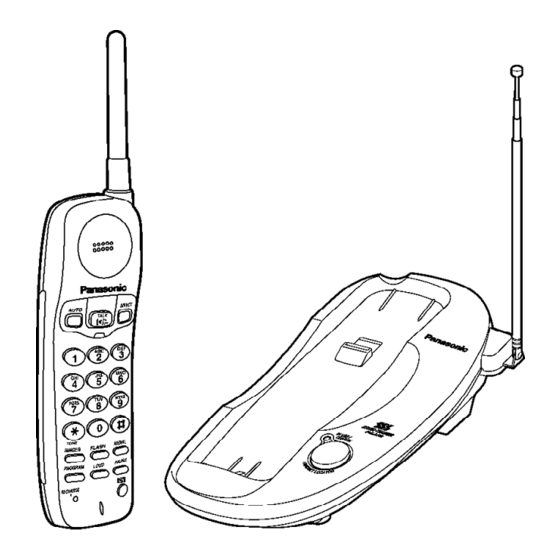
6. LOCATION OF CONTROLS 6.1. Base Unit... - Page 7 6.2. Handset...
- Page 8 7. CONNECTION...
- Page 9 - USE ONLY WITH Panasonic AC ADAPTOR PQLV16BXZ. - The AC adaptor must remain connected at all times. (It is normal for the adaptor to feel warm during use.) - This unit will not function during a power failure. If you want to...
- Page 10 8. OPERATIONS 8.1. Making Calls...
- Page 11 8.2. Answering Calls 8.3. Storing Phone Numbers in Memory...
- Page 12 8.4. Storing a Phone Number in the DIRECT Button 8.5. Dialing a Stored Number...
- Page 13 8.6. Dialing the Stored Number in the DIRECT Button 8.7. Flash Button...
- Page 14 9. DISASSEMBLY INSTRUCTIONS Show in Fig. Procedure To remove. Remove. Lower Cabinet Screws (2.6 × 12)....... (A) × 4 1, 2 Main P.C. Board Screw (2.6 × 6)......(B) × 1 Screw (2.6 × 12)......(C) × 1 Solder Main P.C. Board.
-
Page 15: Troubleshooting Guide
Show in Fig. Procedure To remove. Remove. Rear Cabinet Battery compartment cover. 3, 4 Screws (2.6 × 12)......(D) × 2 3, 4, 5 Follow the procedure. 3, 4, 5, 6 Main P. C. Board Screw (2.6 × 12)......(E) × 1 Tape and solder. -
Page 16: Check Power
Cross Reference: Check Power Bell Reception Check Battery Charge Check Link Check Handset Transmission Check Handset Reception 10.1. Check Power... - Page 17 Cross Reference: Reset Circuit (Base Unit) Power Supply Circuit Note: CPU: IC2 Cross Reference: Charge Circuit Note: CPU: IC2 *: Each measurement points are shown in CIRCUIT BOARD (Base Unit) () or CIRCUIT BOARD (Handset) 10.2. Bell Reception...
-
Page 18: Check Battery Charge
Cross Reference: Check Link Telephone Line Interface Note: CPU: IC2 Cross Reference: Check Link *: Each measurement points are shown in CIRCUIT BOARD (Base Unit) () or CIRCUIT BOARD (Handset) 10.3. Check Battery Charge... - Page 19 Cross Reference: Charge Circuit Power Supply Circuit Note: CPU: IC2 Cross Reference: Reset Circuit (Handset) Note: CPU: IC2...
-
Page 20: Check Link
*: Each measurement points are shown in CIRCUIT BOARD (Base Unit) () or CIRCUIT BOARD (Handset) 10.4. Check Link **: Refer to Adjustment Note: CPU: IC2 RF IC: IC1... - Page 21 *: Each measurement points are shown in CIRCUIT BOARD (Base Unit) () or CIRCUIT BOARD (Handset) **: Refer to Adjustment Note: CPU: IC2 RF IC: IC1...
-
Page 22: Check Handset Transmission
*: Each measurement points are shown in CIRCUIT BOARD (Base Unit) () or CIRCUIT BOARD (Handset) 10.5. Check Handset Transmission Cross Reference: Signal Route 10.6. Check Handset Reception Cross Reference: Signal Route *: Each measurement points are shown in CIRCUIT BOARD (Base Unit) () or CIRCUIT BOARD (Handset) - Page 23 *: Refer to Adjustment 11.1. Test Mode Flow Chart (Base Unit) The operation-flow of Test mode and main check items are shown below. Note: **: Refer to the above table. 11.2. How to change the channel *: Refer to Flow Solder Side View 11.3.
-
Page 24: Adjustment Standard (Base Unit)
Adjustment Test Adjustment *Procedure Items Mode Point RX VCO Confirm so that the reading of the Digital Voltmeter is 0.8V ~ 3.0V. Talk Confirmation TX VCO Adjust T6 so that the reading of the Digital Voltmeter is 2.0V ± 0.2V. Talk Adjustment TX Frequency... - Page 25 12. ADJUSTMENTS (HANDSET) If your unit have below symptoms, adjust or confirm each item using remedy column from the table. Symptom Remedy* The movement of Battery Low Indicator is wrong. Make confirmation in item The base unit does not respond to a call from the handset. Make adjustments in item The base unit does not transmit or the transmit frequency is off.
- Page 26 Note: Refet to CIRCUIT BOARD (Handset) Signal Route 12.2. How to change the channel 12.3. Adjustment...
-
Page 27: Adjustment Standard (Handset)
Adjustment Test Procedure Adjustment Items Mode Point 1. Apply 3.50V between BATT(+) and BATT(-). Battery Low 2. Confirm that there is no flashing of RECHARGE LED. Talk Confirmation 3. Apply 3.40V between BATT(+) and BATT(-). 4. Confirm that there is flashing of RECHARGE LED. 1. -
Page 28: How To Check The Handset Speaker
Note: (A) - (I) is refered to ADJUSTMENTS (HANDSET) (Flow Solder Side View) Note: (A) - (I) is refered to ADJUSTMENTS (HANDSET) 13. RF SPECIFICATION 13.1. Base Unit Item Value Refer to -.* Remarks TX Frequency 46.670 MHz ± 100Hz ADJUSTMENTS (BASE UNIT) (C) at CH3 TX Power... -
Page 30: Frequency Table (Mhz)
15. FREQUENCY TABLE (MHz) BASE UNIT PORTABLE UNIT Channel Transmit Frequency Receive Frequency Transmit Frequency Receive Frequency 46.610 49.670 49.670 46.610 46.630 49.845 49.845 46.630 46.670 49.860 49.860 46.670 46.710 49.770 49.770 46.710 46.730 49.875 49.875 46.730 46.770 49.830 49.830 46.770 46.830 49.890... - Page 31 *: The channel is changed if the noise interferes with the conversation. 16.2. Ringing...
-
Page 32: Changing The Channel
16.3. Changing the Channel... -
Page 33: Ports For Transmitting And Receiving Of Data
16.4. Ports for transmitting and receiving of data Handset: transmitting (TX) ... 36 Pin receiving (RX) ... 4 Pin Base Unit: transmitting (TX) ... 17 Pin receiving (RX) ... 10 Pin 16.5. Waveform of DATA used for cordless transmission and reception... - Page 34 The DATA which is transmitted from the Handset to the Base Unit is combination of DATA 0, DATA 1, PSEUD. The DATA which is transmitted from the Base Unit to the Handset is combination of DATA 0, DATA 1, PSEUD. 16.5.1.
- Page 35 - For example (one of part of data) 17. BLOCK DIAGRAM (BASE UNIT) 18. BLOCK DIAGRAM (HANDSET) 19. CIRCUIT OPERATION 19.1. Outline Base unit consists of the following ICs as shown in BLOCK DIAGRAM. - CPU:IC2 - Controlling the whole system - Forming/analyzing all data signals (ACK, CMD signal etc.*) - All interfaces (ex: LED, KEY, SP, Mic, LCD, Detector Circuit (Charge / Power Down)
-
Page 36: Power Supply Circuit
- first/ second mixer - Amplifier for transmission and reception - Additionally, - Power Supply Circuit - Reset Circuit - Charge Circuit - Telephone Line Interface Circuit Handset consist of the following ICs as shown in BLOCK DIAGRAM. - CPU: IC2 - All data signals (forming/analyzing ACK or CMD signal*) - All interfaces (ex;... - Page 37 Fig. 1 19.3. Reset Circuit (Base Unit) After power supply from AC adaptor, the below circuit is for making reset signal. Refer to the below waveform. Fig. 2 Fig. 3...
-
Page 38: Charge Circuit
19.4. Charge Circuit Circuit Operation: When charging the handset on the base unit, the charge current is as follows; DC (JK2) CHG+(Base) [CHG+(Handset) BATT(1)..Battery..BATT(2) CHG-(Handset)] CHG-(Base) In this way, the CPU on both unit detects the fact that the battery is charged. The charge current is controlled by switching Q24, Q25 of Base Unit. -
Page 39: Telephone Line Interface
19.5. Telephone Line Interface Function: - Bell signal detection - ON/OFF hook and pulse dial circuit - Side tone circuit Bell signal detection and OFF HOOK circuit: In the idle mode, Q103 is open to cut the DC loop current and decrease the ring load. When ring voltage appears at the Tip (T) and Ring (R) leads (When the telephone rings), the AC ring voltage is transferred as follows: JK1 (3): T... - Page 40 waveform after filter like a DTMF generator. 19.7. Transmitter/Receiver Base Unit and Handset are mainly consists of RF(Radio Frequency) IC and CPU. Base Unit and Handset transmit/receive voice signal and data signal through the antenna on carrier frequency. Signal Pass : *Refer to CDL TX/RX in Signal Route 19.7.1.
- Page 41 Frequency modulated RF signal is generated and amplified by RF AMP(Q3, Q4, T5). It pass through the Duplexer DPX1 and radiated from Antenna. The signal is transmitted from the base unit and received by the handset antenna and amplified by RF amplifier (Q1) through DPX1 as shown in BLOCK DIAGRAM (HANDSET) ().
-
Page 42: Signal Route
RX data (from Handset): The data signal from handset (ex: Talk, ACK, COM) is also included in 49 MHz band same as the voice data. After second if filter, the data signal is made square shape by data limiting AMP of the RF IC. RX data is output to CPU (RX Data). - Page 43 The power of handset is supplied by battery. Whenever the battery is recharged or inserted, the impulse at CHG+ becomes Reset signal through Q11, and sent to CPU. Fig. 4 Fig. 5...
-
Page 44: Battery Low / Power Down Detector
20.2. Battery Low / Power Down Detector Circuit Operation: “Battery Low” and “Power Down” are detected by RF IC which check the voltage from battery. Shortly, every detected blocks are inside of RF IC. The detected voltage is as follows; - Battery Low Battery voltage : V(Batt) <... -
Page 45: Cpu Data (Base Unit)
Fig. 6 21. CPU DATA (Base Unit) 21.1. IC2... -
Page 46: Cpu Data (Handset)
22. CPU DATA (Handset) 22.1. IC2... - Page 47 23. RF IC (Base Unit and Handset) 23.1. IC1...
-
Page 48: How To Replace Flat Package Ic
24. HOW TO REPLACE FLAT PACKAGE IC 24.1. Preparation - PbF (: Pb free) Solder - Soldering Iron Tip Temperature of 700°F ± 20°F (370°C ± 10°C) Note: We recommend a 30 to 40 Watt soldering iron. An expert may be able to use a 60 to 80 Watt iron where someone with less experience could overheat and damage the PCB foil. -
Page 49: Cabinet And Electrical Parts Location
Be certain each pin is located over the correct pad on the PCB. 2. Apply flux to all of the pins on the IC. 3. Being careful to not unsolder the tack points, slide the soldering iron along the tips of the pins while feeding enough solder to the tip so that it flows under the pins as they are heated. - Page 50 (BASE UNIT) 26. CABINET AND ELECTRICAL PARTS LOCATION (HANDET)
-
Page 51: Accessories And Packing Materials
27. ACCESSORIES AND PACKING MATERIALS... -
Page 52: Replacement Parts List
28. REPLACEMENT PARTS LIST Note: 1. RTL (Retention Time Limited) The marking (RTL) indicates that the Retention Time is limited for this item. After the discontinuation of this assembly in production, the item will continue to be available for a specific period of time. The retention period of availability depends on the type of assembly and the laws governing parts and product retention. - Page 53 LOWER CABINET (for KX-TC2000SNB) PQKF10597Z2 LOWER CABINET (for KX-TC2000SNS) PQKM10607Z1 UPPER CABINET (for KX-TC2000SNB) PQKM10607Y2 UPPER CABINET (for KX-TC2000SNS) PQSA10105Y ANTENNA PQKL10056Z1 WALL MOUNT ADAPTOR (for KX-TC2000SNB) PQKL10056Z2 WALL MOUNT ADAPTOR (for KX-TC2000SNS) LCBT9300013 FOOT RUBBER 28.1.2. MAIN P.C.BOARD PARTS...
- Page 54 Ref. No. Part No. Part Name & Description Remarks PCB1 PQWPC2000SNH MAIN P.C.BOARD ASS'Y (RTL) (ICS) SA133122409 SA138740C28 SA1S0032402 (TRANSISTORS) BB230024104 TRANSISTOR(SI) SB0I0390601 TRANSISTOR(SI) SB1D0390401 TRANSISTOR(SI) SB1D0390401 TRANSISTOR(SI) SB1D0390401 TRANSISTOR(SI) SB1I0390408 TRANSISTOR(SI) SB1I0390408 TRANSISTOR(SI) SB1I0390408 TRANSISTOR(SI) SB0I0390601 TRANSISTOR(SI) SB1I0390408 TRANSISTOR(SI) BB1M0390401 TRANSISTOR(SI) BB1M0390401...
- Page 55 Ref. No. Part No. Part Name & Description Remarks CL310012JT0 COIL CL310012JT0 COIL CL310012JT0 COIL CL310012JT0 COIL CL310R68JS9 COIL CL310012JS1 COIL DPX1 BDFL0104605 COIL (JACKS) DC72P120018 JACK DC71P120023 JACK (CERAMIC CAPACITORS) CATZ681KC68 CERAMIC CAPACITOR CATZ681KC68 CERAMIC CAPACITOR CB114714205 CERAMIC CAPACITOR (CERAMIC FILTERS) BDFA107MA07 CERAMIC FILTER...
- Page 56 Ref. No. Part No. Part Name & Description Remarks ERJ3GEYJ224 220K ERJ3GEYJ101 ERJ3GEYJ104 100K ERJ3GEYJ223 ERJ3GEYJ563 ERJ3GEYJ103 ERJ3GEYJ103 ERJ3GEYJ104 100K ERJ3GEYJ394 390K ERJ3GEYJ222 2.2K ERJ3GEYJ223 ERJ3GEYJ753 ERJ3GEYJ822 8.2K ERJ3GEYJ152 1.5K ERJ3GEYJ153 ERJ3GEYJ153 ERJ3GEYJ681 ERJ3GEYJ222 2.2K ERJ3GEYJ224 220K ERJ3GEYJ221 ERJ3GEYJ104 100K ERJ3GEYJ223 ERJ3GEYJ104 100K...
- Page 57 Ref. No. Part No. Part Name & Description Remarks R116 ERJ3GEY0R00 R118 ERDS2TJ121 R119 ERJ3GEYJ823 R120 ERJ3GEY0R00 R122 ERJ3GEYJ681 R123 ERJ3GEYJ223 R126 ERJ3GEYJ471 R131 ERJ3GEYJ104 100K R132 ERJ3GEYJ222 2.2K R133 ERJ3GEYJ390 R141 ERJ3GEYJ512 5.1K R142 ERDS2TJ220 R143 ERJ3GEYJ514 510K R144 ERDS2TJ106 R145 ERJ3GEYJ102...
- Page 58 Ref. No. Part No. Part Name & Description Remarks ECUV1H104ZFV ECUV1H102KBV 0.001 ECUV1H104ZFV ECUV1H471JCV 470P ECUV1H471JCV 470P ECUV1C474ZFV 0.47 ECUV1H103KBV 0.01 ECEA1HKA2R2 ECUV1H270JCV ECEA1CKA100 ECUV1H473MDV 0.047 ECUV1H102KBV 0.001 ECEA1HKA2R2 ECUV1H103KBV 0.01 ECUV1H103KBV 0.01 ECUV1E223KBV 0.022 ECUV1H822KBV 0.0082 ECUV1H8R2CCV 8.2 ECUV1H103KBV 0.01 ECUV1H153KBV 0.015 ECUV1H104ZFV ECEA1HKA2R2...
- Page 59 Ref. No. Part No. Part Name & Description Remarks ECUV1H103KBV 0.01 ECUV1H104ZFV ECUV1H220JCV ECEA0JKA102 1000 ECUV1H220JCV ECUV1H271KBV 270P ECUV1C223KBV 0.022 ECUV1E223KBV 0.022 ECUV1H104ZFV ECUV1H104ZFV ECUV1C563KBV 0.056 ECUV1H151JCV 150P ECEA1AKA471 ECUV1H104ZFV ECUV1H104ZFV ECUV1C563KBV 0.056 ECUV1H123KBV 0.012 ECUV1H104ZFV ECUV1H562KBV 0.0056 ECEA1AKA101 ECUV1H103KBV 0.01 ECEA1HKA4R7 ECEA1CKA220 ECUV1H103KBV 0.01...
- Page 60 Ref. No. Part No. Part Name & Description Remarks PQJT10182Z CHARGE TERMINAL PQGT16515Z NAME LABEL (for KX-TC2000SNB) PQGT16501Z NAME LABEL (for KX-TC2000SNS) PQKF10535Z1 REAR CABINET (for KX-TC2000SNB) PQKF10535Z4 REAR CABINET (for KX-TC2000SNS) PQKK10124Z1 BATTERY COVER (for KX-TC2000SNB) PQKK10124Z4 BATTERY COVER (for KX-TC2000SNS)
- Page 61 Ref. No. Part No. Part Name & Description Remarks CL310012JS1 COIL CL310012JS1 COIL CL310012JT0 COIL CL310012JT0 COIL CL310R68JT7 COIL SH590121N75 COIL L200 CL3101R2JS9 COIL DPX1 BDFL0104613 COIL (CONNECTOR) BATT1 DCB002X1164 CONNECTOR (CERAMIC FILTERS) BDFA107MA07 CERAMIC FILTER BDFJ0455E00 CERAMIC FILTER (CRYSTAL OSCILLATORS) BD5H1024501 CRYSTAL OSCILLATOR BD8Z3276800...
- Page 62 Ref. No. Part No. Part Name & Description Remarks ERJ3GEYJ124 120K ERJ3GEYJ223 ERJ3GEYJ104 100K ERJ3GEYJ393 ERJ3GEYJ104 100K ERJ3GEYJ514 510K ERJ3GEYJ222 2.2K ERJ3GEYJ223 ERJ3GEYJ473 ERJ3GEYJ822 8.2K ERJ3GEYJ272 2.7K ERJ3GEYJ222 2.2K ERJ3GEYJ820 ERJ3GEYJ104 100K ERJ3GEYJ221 ERJ3GEYJ122 1.2K ERJ3GEYJ102 ERJ3GEYJ102 ERJ3GEYJ222 2.2K ERJ3GEYJ222 2.2K ERJ3GEYJ331 ERJ3GEYJ222...
- Page 63 Ref. No. Part No. Part Name & Description Remarks R106 ERJ3GEYJ820 R107 ERJ3GEYJ222 2.2K R108 ERJ3GEYJ102 R109 ERJ3GEYJ102 R110 ERJ3GEYJ102 R111 ERJ3GEYJ102 R112 ERJ3GEYJ102 R200 ERJ3GEYJ473 R201 ERJ3GEYJ330 (CAPACITORS) ECEA1AKA470 ECUV1H104ZFV ECUV1H104ZFV ECUV1H102KBV 0.001 ECUV1H104ZFV ECUV1H473MDV 0.047 ECUV1H103KBV 0.01 ECUV1H560JCV ECEA1HKA2R2 ECUV1H270JCV ECUV1H103KBV 0.01...
- Page 64 Ref. No. Part No. Part Name & Description Remarks ECUV1H103KBV 0.01 ECUV1E223KBV 0.022 ECUV1H100DCV 10P ECUV1H103KBV 0.01 ECUV1H050CCV 5P ECUV1H150JCV ECUV1H103KBV 0.01 ECUV1H390JCV ECUV1H100DCV 10P ECUV1H104ZFV ECUV1H390JCV ECEA1AKA101 ECUV1H103KBV 0.01 ECUV1H150JCV ECUV1H150JCV ECUV1H103KBV 0.01 ECUV1H104ZFV ECUV1H104ZFV ECUV1H300JCV ECUV1H300JCV ECUV1H104ZFV ECUV1H104ZFV ECUV1H473MDV 0.047 ECUV1H103KBV 0.01 ECUV1H471JCV...
- Page 65 29. FOR SCHEMATIC DIAGRAM 29.1. Base Unit (SCHEMATIC DIAGRAM (Base Unit)) 1. DC voltage measurements are taken with an oscilloscope or a tester with a ground. 2. The schematic diagrams and circuit board may be modified at any time with the development of new technology. Important Safety Notice: Components identified by mark have special characteristics important...
- Page 66 33.2. Flow Solder Side View G / KXTC2000SNB / KXTC2000SNS...
- Page 67 R0603 R0603 K103 J39P K682 SOT-23\ECB C0603 C0603 C0603 R0603 C0603 C0603 C0603 1160 R0603 SOT-23 R0603 R0603 SOT-23\ECB J39P IFT\7 C0603 J10P C0603 Z104 VCD2 J39P R0603 C0603 R0603 C0603 R0603 R0603 KX-TC2000SNB/SNS SCHEMATIC DIAGRAM (RF Unit (Base Unit))
- Page 68 AUTO K22 DIRT Z104 Z104 C0603 C0603 ROW0 5V6 0.5W SOT-23 D\362 10V 0.5W R111 3.9V to 0V ZD7.5 120 OHM 0603 COIL SMD 0805 While charging SOT-23 VBAT CHG- 12uH L7.5 3.9V BATT1 3V6/300mA CNT2P\2.5 KX-TC2000SNB/SNS SCHEMATIC DIAGRAM (Handset)
- Page 69 R107 R0603 1434 J15P 510K R0603 K103 J10P K103 R0603 R0603 R0603 C0603 C0603 C0603 C0603 R0603 C0603 IFT\7 R0603 SOT-23\EBC R0603 J39P SOT-23\EBC C0603 Z104 J10P VCD2 J39P C0603 C0603 C0603 2.2K R0603 KX-TC2000SNB/SNS SCHEMATIC DIAGRAM (RF Unit (Handset))
- Page 70 R144 R127 J166 R128 R113 J155 J145 J149 R152 J153 J117 J113 J115 J157 J159 J156 J116 D404 KX-TC2000SNB/SNS CIRCUIT BOARD (Component View (Base Unit))
- Page 71 (CPU: 18) TX DATA R100 C108 (CPU: 17) R109 R117 R119 C120 R166 R148 R140 R149 R177 R122 R138 R137 R116 R129 R105 R203 R104 R183 R178 R179 RING DET (CPU: 24) KX-TC2000SNB/SNS CIRCUIT BOARD (Flow Solder Side View (Base Unit))
- Page 72 R109 R101 R106 R105 R107 CHG DET RSSI VDD (CPU: 40) TX DATA TX DATA (CPU: 37) (DV1) Battery Low (CPU: 36) KX-TC2000SNB/SNS CIRCUIT BOARD (Component View (Handset))
- Page 73 2nd Mix TXGND TXPOWER (RF IC: 36) C203 R200 Q200 R201 C201 C202 V Bat IF IN TX VCO (RF IC: 33) (RF IC: 32) KX-TC2000SNB/SNS CIRCUIT BOARD (Flow Solder Side View (Handset))
- Page 74 Marked...
- Page 75 Marked...
- Page 76 FM Deviation Audio Meter Analyzer Frequency Counter Confirmation of VCO voltage RF Volt Meter Volt Meter DC Volt Meter 50Ω T.P ( CH change at test mode) (A), (B) 49.86MHz RX-VCO TX-VCO TXPOWER TXGND R407 Q403 C402 R409 ZD11 R175 R405 R76 R63 R153...
- Page 77 AF Volt Meter (H) 150Ω R109 R101 R106 R105 R107 47µF (A) Battery Low Oscilloscope Generator (G) Noise Squelch...
- Page 78 46.670MHz RF Millivolt Meter 50Ω Frequency Counter Audio (I), (J) FM Deviation Analyzer Meter Volt Meter TXGND TXPOWER C203 R200 Q200 R201 C201 C202 TX VCO DC Volt Meter RX VCO DC Volt Meter DC Power Supply...
- Page 79 RF AMP TX VCO Q3,Q4, T5 Q5, T6, DV1 Q402,Q403 RESET -DATA DATA -CLK Q401 CHARGE -STB CONTROL Q14, Q17 DATA Q24, Q25 DC 12V DC 5V Q21, LED1 CHARGE CHARGE CONTROL LINE TERMINAL AUDIO SIGNAL KX-TC2000SNB/SNS BLOCK DIAGRAM (BASE UNIT)
- Page 80 BATTERY CONTROL 3.9V DIODE BRIDGE RF AMP TX VCO Q5, T5 Q6, T6, DV1 Q200 DIODE CHARGE -DATA DATA RESET BRIDGE TERMINAL -CLK -STB DATA CHARGE IC2 PING37 Q8, LED 1-4 BUZZER Q7, BZ1 KEY BOARD KX-TC2000SNB/SNS BLOCK DIAGRAM (HANDSET)
- Page 81 C0603 4U7/50V IC3D 12VDC 22UF\16V RING DET R149 EC5\5 R0603 200mA EC5\2.5 C0603 SIP14 R0603 ZD7.5 SOT-23 R150 12uH 510K R0603 L7.5 JACK DC C101 R152 R183 0805 VCPU K562 10M 1/4W 10M 0805 C0603 KX-TC2000SNB/SNS SCHEMATIC DIAGRAM (Base Unit)