Chapters
Table of Contents

Related Manuals for LG MUSICflow SJ6


Summary of Contents for LG MUSICflow SJ6
- Page 1 Internal Use Only SMART Hi-Fi AUDIO Wireless Multi-room Sound Bar SERVICE MANUAL MODEL: SJ6 SJ6 (SJ6, SPJ5-W) CAUTION BEFORE SERVICING THE UNIT, READ THE “SAFETY PRECAUTIONS” IN THIS MANUAL. P/NO : AFN77558555 JANUARY, 2017...
- Page 2 CONTENTS SECTION 1 ..SUMMARY SECTION 2 ..CABINET & MAIN CHASSIS SECTION 3 ..ELECTRICAL SECTION 4 ..WIRELESS SUBWOOFER PART...
-
Page 3: Table Of Contents
SECTION 1 SUMMARY CONTENTS PRODUCT SAFETY SERVICING GUIDELINES FOR AUDIO PRODUCTS ............ 1-3 SERVICING PRECAUTIONS ..........................1-4 • GENERAL SERVICING PRECAUTIONS • INSULATION CHECKING PRODEDURE • ELECTROSTATICALLY SENSITIVE (ES) DEVICES WIRELESS SUBWOOFER CONNECTION ....................... 1-5 HIDDEN KEY MODE ............................1-6 PROGRAM UPDATE GUIDE .......................... -
Page 4: Product Safety Servicing Guidelines For Audio Products
When servicing this product, under no circumstances should the original design be modified or altered without permission from LG Corporation. All components should be replaced only with types identical to those in the original circuit and their physical location, wiring and lead dress must conform to original layout upon completion of repairs. -
Page 5: Servicing Precautions
SERVICING PRECAUTIONS CAUTION: Before servicing the Audio products covered by this Electrostatically Sensitive (ES) Devices service data and its supplements and addends, read and fol- Some semiconductor (solid state) devices can be damaged low the SAFETY PRECAUTIONS. easily by static electricity. Such components commonly are NOTE: if unforeseen circumstances create conflict between called Electrostatically Sensitive (ES) Devices. -
Page 6: Wireless Subwoofer Connection
WIRELESS SUBWOOFER CONNECTION LED indicator of wireless subwoofer Note : • It takes a few seconds (and may take longer) for the main unit and the subwoofer to communicate with LED Color Status each other and make sounds. Green • The closer the main unit and the subwoofer, the The connection is trying. -
Page 7: Hidden Key Mode
HIDDEN KEY MODE HIDDEN MODE KEYS MICOM RESET Main unit ' (Volume)' + Remote control 'SOUND EFFECT' for more than 3 seconds. Micom Option Change Main unit ' (Volume)' + Remote control 'NIGHT' for more than 3 seconds. Main unit ' (Volume)' + Remote control ' (Play/Pause)' for more than 3 seconds. -
Page 8: Program Update Guide
PROGRAM UPDATE GUIDE 1. Preparation - Remote control. - Do format USB Memory to FAT32 File system. - USB : Update fi le exist only in the USB Memory stick. Ex ) SJ6 : MAIN E:\DSP_MAIN_SJ6.ROM (if USB driver is E:\) MICOM ... -
Page 9: Lan Update Guide
LAN UPDATE GUIDE 1. Using MP tool 1) Open MP tool and select “Key DN”. 2) Check the section for download and open download fi le. - Page 10 3) Connect PC and SET by cross LAN cable. PC IP setting 192.168.0.1 Subnet: 255.255.254.0 Gateway: 10.168.0.1 4) Set power on. 5) Connect LAN cable to Set and then Press “ADD” key within 3 seconds after connect the LAN. (Please connect the LAN when blinking WiFi-LED after booting) *Download fi...
- Page 11 7) Press “Update” button. 8) Download result display “OK!” if start download. 1-10...
- Page 12 9) You can identify update status by network indicator lamp. White <Updating : blinking white LED> 1-11...
-
Page 13: Software Update Guide
SOFTWARE UPDATE GUIDE 1. Using USB 1-1. MICOM 1) Copy the fi rmware to USB. - Change the fi le name to “MICOM_SJ6.HEX”. 2) Insert USB to USB port. 3) VFD display “UPGRADE”. 4) Press “PLAY/PAUSE” key. 5) VFD display “M-UPDATE”. 6) Set auto power off after updating done. - Page 14 2. Using APP Power on Smart Audio and implement Music Flow App in your smart phone. 1) Connect Speaker. 2) Select red box. 3) Settings -> Version Info. 4) Select Version info. 1-13...
- Page 15 5) Display “Need to update” if there are ※ Display new version info new fi rmware in the server. if you press “Need to update”. 6) Start Update below icon. ※ Display update progress info. ※ Do not power off during update.
- Page 16 7) Display update info. 8) Display “Update is completed” message when Complete update. 1-15...
-
Page 17: Specifications
SPECIFICATIONS • GENERAL Power requirements 25 V 1.52 A (AC adapter) Power consumption Refer to the main label on the unit. Networked standby : 5.8 W (If all network ports are activated.) AC adapter Model : DA-38A25 Manufacturer : Asian Power Devices Inc. Input : 100 - 240 V ~ 50 - 60 Hz Output : 25 V 1.52 A... - Page 18 SECTION 2 CABINET & MAIN CHASSIS CONTENTS DISASSEMBLY INSTRUCTIONS ........................2-2 1. HOW TO DISASSEMBLE THE MAIN UNIT ..................... 2-2 2. HOW TO DISASSEMBLE THE SUBWOOFER ..................2-9 EXPLODED VIEWS ............................2-13 1. MAIN UNIT SECTION ..........................2-13 2. WIRELESS SUBWOOFER SECTION ....................2-15 3.
-
Page 19: Disassembly Instructions
DISASSEMBLY INSTRUCTIONS 1. HOW TO DISASSEMBLE THE MAIN UNIT ※ Before begin, position the Main Unit upside down. 1-1. Case Bottom Assembly 1) Remove the 21 Screws. 2) Remove the Case Bottom Assembly. Case Bottom Assembly Figure 1-1... -
Page 20: How To Disassemble The Main Unit
HOW TO DISASSEMBLE THE MAIN UNIT 1-2. Main Frame Assembly 1) Disconnect the 3 harness cables from the Main PCB. Figure 1-2 (1) 2) Remove the 2 screws. 3) Remove the Main Frame Assembly (Main Chassis + PCBA). Main Frame Assembly Figure 1-2 (2) - Page 21 HOW TO DISASSEMBLE THE MAIN UNIT 1-2-1. Front PCB Assembly 1) Remove the 2 screws. 2) Remove the Front PCB Assembly. Front PCB Assembly Figure 1-2-1 1-2-2. Main PCB Assembly 1) Detach the cables from the Main chassis. 2) Disconnect the FFC cables from the Main PCB. 3) Remove the 5 Screws (Main + HDMI Jack).
- Page 22 HOW TO DISASSEMBLE THE MAIN UNIT 1-2-3. BT and WIRELESS Module 1) Disconnect the FFC cable from the BT module. 2) Remove the BT module. 3) Disconnect the FFC cable from the WIRELESS module. 4) Disconnect the 2 Hooks. 5) Remove the WIRELESS module. BT Module WIRELESS Module Figure 1-2-3...
- Page 23 HOW TO DISASSEMBLE THE MAIN UNIT 1-2-4. WI-FI Module 1) Remove the screw. 2) Disconnect the 2 Hooks. 3) Remove the WI-FI module. 4) Disconnect the FFC cable from the WI-FI module. WI-FI Module Figure 1-2-4...
- Page 24 HOW TO DISASSEMBLE THE MAIN UNIT 1-3. SPEAKER CHAMBER L/R Assembly 1) Remove the Speaker Chamber L/R Assembly. Speaker Chamber Right Assembly Speaker Chamber Left Assembly Figure 1-3 1-4. KEY PCB Assembly 1) Remove the KEY PCB Assembly. KEY PCB Assembly Figure 1-4...
- Page 25 HOW TO DISASSEMBLE THE MAIN UNIT 1-5. How to organize cables When assembling, place the cables (Speaker network cables and Key cable) as shown in the fi gure below. Figure 1-5 (1). < Harness cable from KEY PCB to MAIN PCB > Figure 1-5 (2).
- Page 26 2. HOW TO DISASSEMBLE THE SUBWOOFER 2-1. Rear Panel Assembly 1) Remove the 13 screws. Figure 2-1 (1) 2) Pull out the Rear Panel Assembly and disconnect the SPK cable. Rear Panel Assembly SPK cable Figure 2-1 (2)
-
Page 27: How To Disassemble The Subwoofer
HOW TO DISASSEMBLE THE SUBWOOFER 2-2. WIRELESS Module 1) Disconnect the FFC cable. 2) Remove the EVA sheet (0.15T) covered the WIRELESS module. 3) Remove the WIRELESS module. 4) Remove the EVA gasket (1.0T) covered the WIRELESS module. AMP+SMPS PCB Assembly Figure 2-2 (1) Caution when assembling the WIRELESS Module 1) Attach the EVA gaskets (1.0T) to both sides of the WIRELESS module. - Page 28 HOW TO DISASSEMBLE THE SUBWOOFER 2-3. AMP+SMPS PCB Assembly 1) Disconnect the Power inlet socket cable. AMP+SMPS PCB Assembly Figure 2-3 (1) 2) Remove the 5 screws. 3) Remove the AMP+SMPS PCB Assembly. AMP+SMPS PCB Assembly Figure 2-3 (2) 2-11...
- Page 29 2-12...
-
Page 30: Exploded Views
EXPLODED VIEWS 1. MAIN UNIT SECTION NOTES) THE EXCLAMATION POINT WITHIN AN EQUILATERAL TRIANGLE IS INTENDED TO ALERT THE SERVICE PERSONNEL TO THE PRESENCE OF IMPORTANT SAFETY INFORMATION IN SERVICE A80R LITERATURE. MAIN FRONT 271R LCD401 Wi-Fi CABLE1 A80L CABLE2 CABLE4 CABLE3 WIRELESS... -
Page 31: Wireless Subwoofer Section
2. WIRELESS SUBWOOFER SECTION A900 A900W A45W A54W 2-15 2-16... -
Page 32: Packing Accessory Section
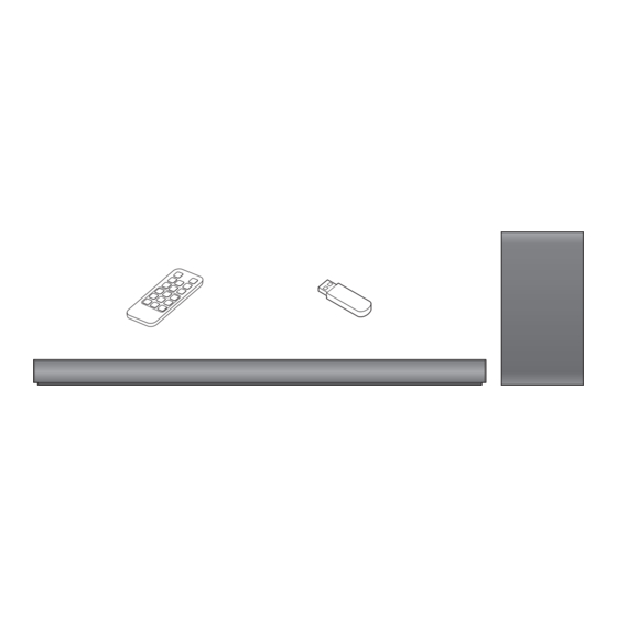
3. PACKING ACCESSORY SECTION Optional Part 801 Owner’s manual 806 Optical cable 900 Remote control 808 Batteries (2) 300 Power cord 833 AC adapter 836 Screws (2) 835 Wall bracket 803 Packing, Main 829 Cable tie 804 Bag 802 Box 2-17... - Page 33 2-18...
- Page 34 SECTION 3 ELECTRICAL CONTENTS WIRING DIAGRAM ............................3-2 BLOCK DIAGRAMS ............................3-3 1. SYSTEM BLOCK DIAGRAM ........................3-3 2. POWER BLOCK DIAGRAM ........................3-4 ONE POINT REPAIR GUIDE ..........................3-5 1. NO BOOTING WHEN YOU TURN THE UNIT ON, NO MESSAGE OR “HELLO” ON FRONT PANEL ..........................
-
Page 35: Wiring Diagram
WIRING DIAGRAM... -
Page 36: Block Diagrams
BLOCK DIAGRAMS 1. SYSTEM BLOCK DIAGRAM... -
Page 37: Power Block Diagram
2. POWER BLOCK DIAGRAM... -
Page 38: One Point Repair Guide
ONE POINT REPAIR GUIDE 1. NO BOOTING WHEN YOU TURN THE UNIT ON, NO MESSAGE OR “HELLO” ON FRONT PANEL When you turn on your set, no message on the front panel, and stand-by LED doesn’t work. 1-1. IC302 System 12 VA (No 12 VA) 1-1-1. - Page 39 ONE POINT REPAIR GUIDE NO BOOTING WHEN YOU TURN THE UNIT ON, NO MESSAGE OR “HELLO” ON FRONT PANEL When you turn on your set, it will blank / no message on front panel, and stand-by LED doesn’t work. 1-2. IC301 System 3.3 V (No 3.3 VA) 1-2-1.
- Page 40 ONE POINT REPAIR GUIDE NO BOOTING WHEN YOU TURN THE UNIT ON, NO MESSAGE OR “HELLO” ON FRONT PANEL When you turn on your set, it will blank / no message on front panel, and stand-by LED doesn’t work. 1-3. LCD System power 5 V, 3.3 VA (No 5 V, 3.3 VA) 1-3-1.
- Page 41 ONE POINT REPAIR GUIDE 2. NO SOUND 2-1. BLUETOOTH 2-1-1. Solution Replace MAIN board. 2-1-2. How to troubleshoot (Countermeasure) 1) Please check status of Bluetooth cable connection. (at CN104 and BT module) 2) Please check 3.3 VA (at pin1 of CN104). If 3.3 V is OK, please check BT_RST, BT_UART_RX,BT_UART_TX, BT_SCL, BT_SDA (pin2, 4, 11, 12).
-
Page 42: Sound
ONE POINT REPAIR GUIDE NO SOUND 2-2. OPTICAL 2-2-1. Solution Replace MAIN board. 2-2-2. How to troubleshoot (Countermeasure) 1) Please check 3.3 VA at FB203. 2) If 3.3 VA is ok, please check OPT_IN signal (R207) when optical mode. 3) If signal is abnormal, replace MAIN board. 2-2-3. - Page 43 ONE POINT REPAIR GUIDE NO SOUND 2-3. HDMI 2-3-1. Solution Replace MAIN board. 2-3-2. How to troubleshoot (Countermeasure) 1) Please check soldering status of HDMI jack and check HDMI_5.1VA at IC308 pin1. 2) If soldering status and 5.1 VA are abnormal, replace MAIN board. 2-3-3.
- Page 44 ONE POINT REPAIR GUIDE NO SOUND 2-4. PORTABLE 2-4-1. Solution Replace MAIN board. 2-4-2. How to troubleshoot (Countermeasure) 1) Please check the soldering status of portable jack and check IC200 pin3 (VCC_5V), pin4 (D_3.3V). 2) If portable jack and voltage has abnormal status, replace MAIN board. 2-4-3.
- Page 45 ONE POINT REPAIR GUIDE 3. PROTECTION ERROR No display or No Sound. 3-1. D(DC) PROTECTION 3-1-1. Solution Replace MAIN board. 3-1-2. How to troubleshoot (Countermeasure) 1) Check DC Voltage of speaker out FL+/- , TWL+/- (CN703 pin1, 2, 3, 4), FR+/-, TWR+/- (CN704 pin1, 2, 4, 5). 2) Check resistor crack, cold solder of PWM IC out (R607, R608, R602, R603, R612, R613, R609, R611).
-
Page 46: Protection Error
ONE POINT REPAIR GUIDE PROTECTION ERROR No display or No Sound. 3-2. S(SHUT DOWN) PROTECTION 3-2-1. Solution Replace MAIN board. 3-2-2. How to troubleshoot (Countermeasure) 1) Check PVDD voltage (25 V) of IC700, IC701 pin29, 30, 31, 36, 37, 38. - If PVDD voltage has 8.5 V under, refer to STEP 1-1. - Page 47 ONE POINT REPAIR GUIDE PROTECTION ERROR No display or No Sound. 3-3. B(BURNT) PROTECTION 3-3-1. Solution Replace MAIN board. 3-3-2. How to troubleshoot (Countermeasure) 1) Check voltage 12 V of IC700, IC701 at pin1 ~ 2, if 12 V has problem refer to STEP 1-1. 2) If 12 V is OK, replace MAIN board.
-
Page 48: Waveforms Of Major Check Point
WAVEFORMS OF MAJOR CHECK POINT 1. CRYSTAL FIG 1-1. X501 (27 MHz) FIG 1-2. X600 (24.576 MHz) 2. FLASH MEMORY FIG 2. VCC, CS#, CLK, DO 3-15... -
Page 49: Tact Key
3. TACT KEY 1 ~ 1.13 V 0.72 ~ 0.82 V FIG 3-2. Press FUNC Key FIG 3-1. Press Power Key 0.424 ~ 0.485 V FIG 3-3. Press - Key FIG 3-4. Press + Key 3-16... -
Page 50: Remote Control
4. REMOTE CONTROL FIG 4-1. Input Voltage FIG 4-2. Low Timing Item Measured Spec. IR Receiver Spec: Input Level 3.3 V 2.7 ~ 5.5 V “ Low” Timing 4.4 ms 3.6 ms ~ 5.04 ms “ High” Timing 4.48 ms 4.08 ms ~ 5.04 ms FIG 4-3. -
Page 51: Optical
5. OPTICAL FIG 5-1. OPT_IN FIG 5-2. OPT_DET 3-18... -
Page 52: Portable
6. PORTABLE FIG 6-1. ADC IC 5 V FIG 6-2. ADC IC 3.3 V 1 1 .27 Vrms FIG 6-3. Analog Input Voltage 3-19... - Page 53 3-20...
-
Page 54: Circuit Voltage Chart
CIRCUIT VOLTAGE CHART 1. ICs VOLTAGE Location/ Name IC Name/ Type Vcc/ Vdd Location/ Name IC Name/ Type Vcc/ Vdd Location/ Name IC Name/ Type Vcc/ Vdd • Spec: • Spec: • Spec: TYPE: 48P IC100 VDD: +1.8V~+5.5V VIN: +4.5V~+17V VDD_IO: VENDER: RENESAS TYPE: 6P... -
Page 55: Capacitor Voltage
2. CAPACITOR VOLTAGE Location No. Spec. DV Real Value(#1,#2)/V C703 C734 330uF/35V 25.52 25.52 25.51 25.52 25.52 C738 C769 CE301 330uF/35V 25.53 25.52 25.52 25.53 25.52 3. CONNECTOR VOLTAGE CN100 (MAIN <-> Wireless) Power MAIN Wireless module SPEC WL_3V3 3.308V 3.311V 3.3V(3.15~3.45V) CN104 (MAIN <->... -
Page 56: Printed Circuit Board Diagrams
PRINTED CIRCUIT BOARD DIAGRAMS 1. MAIN P. C. BOARD DIAGRAM (TOP VIEW) (BOTTOM VIEW) 3-25 3-26... -
Page 57: Front P. C. Board Diagram
2. FRONT P. C. BOARD DIAGRAM (TOP VIEW) (BOTTOM VIEW) 3. KEY P. C. BOARD DIAGRAM (TOP VIEW) (BOTTOM VIEW) 3-27 3-28... - Page 58 SECTION 4 WIRELESS SUBWOOFER PART CONTENTS WIRING DIAGRAM ............................4-2 BLOCK DIAGRAM ............................4-3 ONE POINT REPAIR GUIDE ..........................4-4 1. POWER ON ERROR ..........................4-4 2. WIRELESS CONNECTION ........................4-6 WAVEFORMS OF MAJOR CHECK POINT ...................... 4-7 1. CRYSTAL ..............................4-7 2.
-
Page 59: Wiring Diagram
WIRING DIAGRAM 2P, 3.96mm ST, Non Lock SMD Wireless 26P, 0.5mm ST, Non Lock SMD 2P, 3.96mm ST, Non Lock , SMD Power... -
Page 60: Block Diagram
BLOCK DIAGRAM Wireless LED (RED, GREEN) Wireless AMP_PDN AMP_SD PAIRING Reset KEY SW+/SW- PWM IC AMP IC... -
Page 61: One Point Repair Guide
ONE POINT REPAIR GUIDE 1. POWER ON ERROR Fundamental power check points. 1-1. 12 V 1) Check 12 V at WL708. 2) If 12 V is not checked at the point, then find PVDD at pin7 of WIC704. 3) 1), 2) is NG Replace WIC704. If you can’t check PVDD voltage, then replace the PCB board. - Page 62 ONE POINT REPAIR GUIDE POWER ON ERROR Fundamental power check points. 1-3. 3.3 VA 1) Check 3.3 VA at pin1 of WIC703. 2) Check 3.3V_PWM at pin6 of WIC703. 3) 1), 2) is NG Replace WIC703. If you can’t check PVDD voltage, then replace the PCB board. WIC703 WIC703 <...
-
Page 63: Wireless Connection
ONE POINT REPAIR GUIDE 2. WIRELESS CONNECTION Wireless connection malfunction. 2-1. 3.3 VA 1) Check 3.3 VA at WFB604. 2-2. Connection 1) Wireless module connection closely. 2) Implement Wireless Factory Reset. MAIN SET : Soundbar vol MIN and push Mute key (sustain 3 ~ 5 seconds). ... -
Page 64: Waveforms Of Major Check Point
WAVEFORMS OF MAJOR CHECK POINT 1. CRYSTAL FIG 1. WX601 (24.576 MHz) 2. FLASH MEMORY FIG 2. VCC, CS#, CLK, DO... -
Page 65: Voltage
3. VOLTAGE FIG 3-2. Woofer 12 VA FIG 3-1. Woofer PVDD FIG 3-3. Woofer 3.3 VA FIG 3-4. Woofer 3.3V_PWM... -
Page 66: Amp Voltage
4. AMP VOLTAGE FIG 4-2. AMP_12V FIG 4-1. AMP PVDD... -
Page 67: Pwm
5. PWM FIG 5-2. Woofer PWM SW- Signal FIG 5-1. Woofer PWM SW+ Signal 4-10... -
Page 68: Led
6. LED FIG 6-2. Pairing On Status Green LED FIG 6-1. Pairing Off Status Red LED 4-11... - Page 69 4-12...
-
Page 70: Circuit Voltage Chart
CIRCUIT VOLTAGE CHART Location No. Description Pin Number Specifi cation Real Value (#1, #2) VDD _IO: VDD_IO: 3.37 V 3.37 V #17, 43, 52 2.97 V ~ 3.63 V VDD_CORE: VDD_CORE: WIC601 Sound/Audio 1.27 V 1.27 V #6, 25, 63 1.08 V ~ 1.32 V Processor VDD_PLL:... -
Page 71: Printed Circuit Board Diagrams
PRINTED CIRCUIT BOARD DIAGRAMS 1. WOOFER SMPS & AMP P. C. BOARD (TOP VIEW) (BOTTOM VIEW) NOTE) Warning Parts that are critical with respect to risk of fire or electrical shock. 4-15 4-16...