Table of Contents
Advertisement
Quick Links
Telephone Equipment
KX-TG6381LBB
Model No.
KX-TG6381LBS
KX-TG6382LBB
KX-TGA632LBB
KX-TGA632LBS
Expandable Digital Cordless Phone
Black Version
Pearl Silver Version
(for Brazil)
© 2008 Panasonic Communications Co., Ltd. All
rights reserved. Unauthorized copying and distribu-
tion is a violation of law.
ORDER NO. KM40807637CE
Advertisement
Table of Contents
Troubleshooting

Related Manuals for Panasonic KX-TG6381LBB


Summary of Contents for Panasonic KX-TG6381LBB
- Page 1 ORDER NO. KM40807637CE Telephone Equipment KX-TG6381LBB Model No. KX-TG6381LBS KX-TG6382LBB KX-TGA632LBB KX-TGA632LBS Expandable Digital Cordless Phone Black Version Pearl Silver Version (for Brazil) © 2008 Panasonic Communications Co., Ltd. All rights reserved. Unauthorized copying and distribu- tion is a violation of law.
- Page 2 KX-TG6381LBB/KX-TG6381LBS/KX-TG6382LBB/KX-TGA632LBB/KX-TGA632LBS...
-
Page 3: Table Of Contents
KX-TG6381LBB/KX-TG6381LBS/KX-TG6382LBB/KX-TGA632LBB/KX-TGA632LBS TABLE OF CONTENTS PAGE PAGE 1 Safety Precautions----------------------------------------------- 4 15.2. CPU Data (Handset) ------------------------------------ 84 1.1. For Service Technicians --------------------------------- 4 15.3. How to Replace the Flat Package IC --------------- 85 2 Warning -------------------------------------------------------------- 4 15.4. How to Replace the LLP (Leadless Leadframe 2.1. -
Page 4: Safety Precautions
KX-TG6381LBB/KX-TG6381LBS/KX-TG6382LBB/KX-TGA632LBB/KX-TGA632LBS 1 Safety Precautions 1.1. For Service Technicians • Repair service shall be provided in accordance with repair technology information such as service manual so as to pre- vent fires, injury or electric shock, which can be caused by improper repair work. -
Page 5: Discarding Of P. C. Board
KX-TG6381LBB/KX-TG6381LBS/KX-TG6382LBB/KX-TGA632LBB/KX-TGA632LBS 2.2.1. Suggested PbF Solder There are several types of PbF solder available commercially. While this product is manufactured using Tin, Silver, and Copper (Sn+Ag+Cu), you can also use Tin and Copper (Sn+Cu), or Tin, Zinc, and Bismuth (Sn+Zn+Bi). Please check the manufac- turer's specific instructions for the melting points of their products and any precautions for using their product with other materi- als. -
Page 6: Specifications
KX-TG6381LBB/KX-TG6381LBS/KX-TG6382LBB/KX-TGA632LBB/KX-TGA632LBS 3 Specifications Note: • Design and specifications are subject to change without notice. -
Page 7: Technical Descriptions
KX-TG6381LBB/KX-TG6381LBS/KX-TG6382LBB/KX-TGA632LBB/KX-TGA632LBS 4 Technical Descriptions 4.1. US-DECT Description The frequency range of 1.92 GHz-1.93 GHz is used. Transmitting and receiving carrier between base unit and handset is same fre- quency. Refer to Frequency Table (P.64). 4.1.1. TDD Frame Format 4.1.2. TDMA system This system is the cycles of 10 ms, and has 6 duplex paths, but maximum duplex communication path is 5 because of dummy bearer use. - Page 8 KX-TG6381LBB/KX-TG6381LBS/KX-TG6382LBB/KX-TGA632LBB/KX-TGA632LBS 4.1.3. Signal Flowchart in the Radio Parts Reception A voice signal from TEL line is encoded to digital data "TXDATA" by DSP (IC501) in a base unit. Then TXDATA goes to RF PART, and it's modulated to 1.9 GHz. The RF signal is amplified and fed to a selected antenna.
-
Page 9: Block Diagram (Base Unit_Main)
KX-TG6381LBB/KX-TG6381LBS/KX-TG6382LBB/KX-TGA632LBB/KX-TGA632LBS 4.2. Block Diagram (Base Unit_Main) -
Page 10: Block Diagram (Base Unit_Rf Part)
KX-TG6381LBB/KX-TG6381LBS/KX-TG6382LBB/KX-TGA632LBB/KX-TGA632LBS 4.3. Block Diagram (Base Unit_RF Part) -
Page 11: Circuit Operation (Base Unit)
KX-TG6381LBB/KX-TG6381LBS/KX-TG6382LBB/KX-TGA632LBB/KX-TGA632LBS 4.4. Circuit Operation (Base Unit) General Description: (DSP, EEPROM) is a digital speech/signal processing system that implements all the functions of speech compression and memory management required in a digital telephone. The DSP system is fully controlled by a host processor DSP. The host processor provides activation and control of all that func- tions as follows. - Page 12 KX-TG6381LBB/KX-TG6381LBS/KX-TG6382LBB/KX-TGA632LBB/KX-TGA632LBS 4.4.3. Power Supply Circuit Function: The power supply voltage from AC adaptor is converted to the desired voltage of each block. Circuit Operation: • Q300 and IC300: 4.0 V DCDC Converter • IC331: 3.3 V Regulator...
- Page 13 KX-TG6381LBB/KX-TG6381LBS/KX-TG6382LBB/KX-TGA632LBB/KX-TGA632LBS 4.4.3.1. Charge Circuit The voltage from the AC adaptor is supplied to the charge circuits.
- Page 14 KX-TG6381LBB/KX-TG6381LBS/KX-TG6382LBB/KX-TGA632LBB/KX-TGA632LBS 4.4.4. Reset Circuit Function: This circuit is used to initialize the microcomputer when it incorporates an AC adaptor. Circuit Operation: When the AC Adaptor is inserted into the unit, then the voltage is shifted by IC331 and power is supplied to the DSP.
- Page 15 KX-TG6381LBB/KX-TG6381LBS/KX-TG6382LBB/KX-TGA632LBB/KX-TGA632LBS 4.4.5. Telephone Line Interface Telephone Line Interface Circuit: Function • Bell signal detection • ON/OFF hook and pulse dial circuit • Side tone circuit Bell signal detection and OFF HOOK circuit: In the idle mode, Q141 is open to cut the DC loop current and decrease the ring load. When ring voltage appears at the Tip (T) and Ring (R) leads (When the telephone rings), the AC ring voltage is transferred as follows: T →...
- Page 16 KX-TG6381LBB/KX-TG6381LBS/KX-TG6382LBB/KX-TGA632LBB/KX-TGA632LBS 4.4.6. Parallel Connection Detect Circuit Function: In order to disable call waiting and stutter tone functions when using telephones connected in parallel, it is necessary to have a circuit that judges whether a telephone connected in parallel is in use or not. This circuit determines whether the telephone con- nected in parallel is on hook or off hook by detecting changes in the T/R voltage.
- Page 17 KX-TG6381LBB/KX-TG6381LBS/KX-TG6382LBB/KX-TGA632LBB/KX-TGA632LBS 4.4.7. Calling Line Identification (Caller ID) Function: The caller ID is a chargeable ID which the user of a telephone circuit obtains by entering a contract with the telephone company to utilize a caller ID service. For this reason, the operation of this circuit assumes that a caller ID service contract has been entered for the circuit being used.
-
Page 18: Block Diagram (Handset)
KX-TG6381LBB/KX-TG6381LBS/KX-TG6382LBB/KX-TGA632LBB/KX-TGA632LBS 4.5. Block Diagram (Handset) IC541 ANT1 ANT2 X501 EEPROM 13.824 MHz Q531 CHG_DET CHARGE DETECT Q362, Q364 RF part CHARGE CHG_CTL CONTROL SYN_OUT SYN_EN SYN_CLK RESET SYN_DATA Q361 D361 SLOT_CTROL CHARGE RADIO_EN IC374 TXDATA RXDATA IC371 2.7 V V_PA... -
Page 19: Block Diagram (Handset_Rf Part)
KX-TG6381LBB/KX-TG6381LBS/KX-TG6382LBB/KX-TGA632LBB/KX-TGA632LBS 4.6. Block Diagram (Handset_RF Part) -
Page 20: Circuit Operation (Handset)
KX-TG6381LBB/KX-TG6381LBS/KX-TG6382LBB/KX-TGA632LBB/KX-TGA632LBS 4.7. Circuit Operation (Handset) 4.7.1. Construction The circuit mainly consists of DSP and RF part as shown in the block diagram. 4.7.1.1. DSP: IC501 Function • Battery Low, Power down detect circuit • Ringer Generation • Interface circuit RF part, Speaker, Mic, LED, Key scan, LCD... - Page 21 KX-TG6381LBB/KX-TG6381LBS/KX-TG6382LBB/KX-TGA632LBB/KX-TGA632LBS 4.7.2. Power Supply Circuit Voltage is supplied separately to each block.
- Page 22 KX-TG6381LBB/KX-TG6381LBS/KX-TG6382LBB/KX-TGA632LBB/KX-TGA632LBS 4.7.3. Charge Circuit When the handset is put on the cradle of the base unit, the power is supplied from CHARGE+ and CHARGE- terminals to charge the battery via R366 or Q361. The voltage between CHARGE+ and CHARGE- flows Q531 → pin 38 of IC501, where the charge is detected.
- Page 23 KX-TG6381LBB/KX-TG6381LBS/KX-TG6382LBB/KX-TGA632LBB/KX-TGA632LBS 4.7.5. Sending Signal The voice signal from the microphone is input to DSP (90, 91). Also the power for the microphone is supplied from DSP (92) and the power is turned OFF on standby. 4.7.6. Reception Signal The voice signal from the base unit is output to DSP (98). This signal is led to R435 and drives the speaker, and the other signal...
-
Page 24: Circuit Operation (Rf Part)
KX-TG6381LBB/KX-TG6381LBS/KX-TG6382LBB/KX-TGA632LBB/KX-TGA632LBS 4.8. Circuit Operation (RF Part) General Description: RF part includes Transmitter and Receiver functions. Digital signals (Mainly voice data) that come from DSP, are modulated and are transmitted. On the other hand, received signals are demodulated and go out to DSP. -
Page 25: Circuit Operation (Charger Unit)
KX-TG6381LBB/KX-TG6381LBS/KX-TG6382LBB/KX-TGA632LBB/KX-TGA632LBS 4.9. Circuit Operation (Charger Unit) The voltage from the AC adaptor is supplied to the charge circuits. Main charge (180~250 mA at the Battery) of maximum 7- hours is started soon after the handset is placed on the charger unit. Then it changes to Trickle charge to prevent from over- charging. -
Page 26: Signal Route
KX-TG6381LBB/KX-TG6381LBS/KX-TG6382LBB/KX-TGA632LBB/KX-TGA632LBS 4.10. Signal Route RF part signal route... -
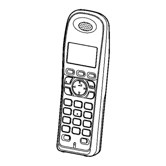
Page 27: Location Of Controls And Components
KX-TG6381LBB/KX-TG6381LBS/KX-TG6382LBB/KX-TGA632LBB/KX-TGA632LBS 5 Location of Controls and Components 5.1. Controls 5.1.2. Handset 5.1.1. Base Unit 5.2. Display... -
Page 28: Installation Instructions
KX-TG6381LBB/KX-TG6381LBS/KX-TG6382LBB/KX-TGA632LBB/KX-TGA632LBS 6 Installation Instructions 6.1. Connections 6.2. Battery 6.2.1. Battery Installation and Replacement... - Page 29 KX-TG6381LBB/KX-TG6381LBS/KX-TG6382LBB/KX-TGA632LBB/KX-TGA632LBS 6.2.3. Battery Level 6.2.4. Panasonic Ni-MH Battery Performance (supplied batteries) 6.2.2. Battery Charge Note for service: The battery strength may not be indicated correctly if the battery is disconnected and connected again, even after it is fully charged. In that case, by recharging the battery as mentioned above, you will get a correct indication of the battery strength.
-
Page 30: Operating Instructions
KX-TG6381LBB/KX-TG6381LBS/KX-TG6382LBB/KX-TGA632LBB/KX-TGA632LBS 7 Operating Instructions 7.1. Programmable Settings 7.1.1. Programming by Scrolling through the Display Menus... - Page 31 KX-TG6381LBB/KX-TG6381LBS/KX-TG6382LBB/KX-TGA632LBB/KX-TGA632LBS 7.1.2. Programming using the Direct Commands...
-
Page 32: Dial Lock
KX-TG6381LBB/KX-TG6381LBS/KX-TG6382LBB/KX-TGA632LBB/KX-TGA632LBS 7.2. Dial Lock For Service Hint: *: If the current password is forgotten, refer to Dial Lock in Troubleshooting (P.34). -
Page 33: Error Messages
KX-TG6381LBB/KX-TG6381LBS/KX-TG6382LBB/KX-TGA632LBB/KX-TGA632LBS 7.3. Error Messages... -
Page 34: Troubleshooting
KX-TG6381LBB/KX-TG6381LBS/KX-TG6382LBB/KX-TGA632LBB/KX-TGA632LBS 7.4. Troubleshooting... - Page 35 KX-TG6381LBB/KX-TG6381LBS/KX-TG6382LBB/KX-TGA632LBB/KX-TGA632LBS...
- Page 36 KX-TG6381LBB/KX-TG6381LBS/KX-TG6382LBB/KX-TGA632LBB/KX-TGA632LBS...
-
Page 37: Test Mode
KX-TG6381LBB/KX-TG6381LBS/KX-TG6382LBB/KX-TGA632LBB/KX-TGA632LBS 8 Test Mode 8.1. Adjustment and Test Mode Flow Chart 8.1.1. TX-CW Mode for Base Unit Note: (*1) When you check test mode, connect to the external Buttons because Base Unit has only LOCATOR key. Refer to Bottom View (P.76). - Page 38 KX-TG6381LBB/KX-TG6381LBS/KX-TG6382LBB/KX-TGA632LBB/KX-TGA632LBS 8.1.2. Test Link Mode for Base Unit Note: (*1) When you check test mode, connect to the external Buttons because Base Unit has only LOCATOR key. Refer to Bottom View (P.76). (*2) Refer to Test Link Mode for Handset (P.42). If you can not proceed to the next step, refer to Registering a Handset to a Base Unit (P.49).
- Page 39 KX-TG6381LBB/KX-TG6381LBS/KX-TG6382LBB/KX-TGA632LBB/KX-TGA632LBS 8.1.3. Adjustment Mode for Base Unit Cross Reference Check and Adjust Frequency (Base Unit) (P.61) Note: (*1) When you check test mode, connect to the external Buttons because Base Unit has only LOCATOR key. Refer to Bottom View (P.76).
- Page 40 KX-TG6381LBB/KX-TG6381LBS/KX-TG6382LBB/KX-TGA632LBB/KX-TGA632LBS 8.1.4. TX-CW Mode for Handset Note: (*1) LCD displays the Channel number. (exception: default/ CH00 = 0ch.) (*2) Refer to Check Table for RF part (P.51).
- Page 41 KX-TG6381LBB/KX-TG6381LBS/KX-TG6382LBB/KX-TGA632LBB/KX-TGA632LBS 8.1.5. RX-CW Test Mode for Handset Note: (*1) LCD displays the Channel number. (exception: default/ CH00 = 0ch.) (*2) Refer to Check Table for RF part (P.51).
- Page 42 KX-TG6381LBB/KX-TG6381LBS/KX-TG6382LBB/KX-TGA632LBB/KX-TGA632LBS 8.1.6. Test Link Mode for Handset Note: (*1) LCD displays the Channel number. (exception: default/ CH00 = 0ch.) (*2) If can not proceed to the next step, refer to Registering a Handset to a Base Unit (P.49). (*3) for factory use only.
- Page 43 KX-TG6381LBB/KX-TG6381LBS/KX-TG6382LBB/KX-TGA632LBB/KX-TGA632LBS 8.1.7. Adjustment Mode for Handset Cross Reference (*1) Adjust Battery Low Detector Voltage (Handset) (P.61) Note: (*2) These are the default values. (*3) These values may not be fixed depending on the battery strength.
-
Page 44: Service Mode
KX-TG6381LBB/KX-TG6381LBS/KX-TG6382LBB/KX-TGA632LBB/KX-TGA632LBS 9 Service Mode 9.1. How to Clear User Setting Units are reset to the Factory settings by this operation (Erase stored Phone numbers, Caller list and etc.). This operation should not be performed for a usual repair. 9.1.1. Handset Note: (*1) Be sure to short the battery terminals of the handset with a lead wire, etc. -
Page 45: Troubleshooting Guide
KX-TG6381LBB/KX-TG6381LBS/KX-TG6382LBB/KX-TGA632LBB/KX-TGA632LBS 10 Troubleshooting Guide 10.1. Troubleshooting Flowchart Cross Reference: Check Power (P.46) Check Battery Charge (P.46) Check Link (P.47) Check the RF part (P.48) Check Handset Transmission (P.55) Check Handset Reception (P.55) Check Caller ID (P.55) - Page 46 KX-TG6381LBB/KX-TG6381LBS/KX-TG6382LBB/KX-TGA632LBB/KX-TGA632LBS 10.1.1. Check Power Cross Reference: Note: Power Supply Circuit (P.12) DSP is IC501. Reset Circuit (P.14) (*1) Refer to Specifications (P.6) for part number and sup- ply voltage of AC adaptor. (*2) Refer to Circuit Board (Base Unit_Main) (P.75).
- Page 47 KX-TG6381LBB/KX-TG6381LBS/KX-TG6382LBB/KX-TGA632LBB/KX-TGA632LBS 10.1.3. Check Link Cross Reference: Note: Check the RF part (P.48) DSP is IC501. (*1) Refer to Finding out the Defective part (P.48).
- Page 48 KX-TG6381LBB/KX-TG6381LBS/KX-TG6382LBB/KX-TGA632LBB/KX-TGA632LBS 10.1.4. Check the RF part 10.1.4.1. Finding out the Defective part After All the Checkings or Repairing 1. Re-register the checked handset to the checked base unit, and Regular HS to Regular BU. Note: (*1) HS: Handset (*2) BU: Base Unit...
- Page 49 KX-TG6381LBB/KX-TG6381LBS/KX-TG6382LBB/KX-TGA632LBB/KX-TGA632LBS 10.1.4.1.1. Registering a Handset to a Base Unit 10.1.4.1.2. Deregistering a Handset 10.1.4.1.3. Deregistering All Handsets by the Base Unit...
- Page 50 KX-TG6381LBB/KX-TG6381LBS/KX-TG6382LBB/KX-TGA632LBB/KX-TGA632LBS 10.1.4.2. RF Check Flowchart Each item (1 ~ 6) of RF Check Flowchart corresponds to Check Table for RF part (P.51). Please refer to the each item. Note: (*1) Refer to Things to Do after Replacing IC or X’tal (P.61).
- Page 51 KX-TG6381LBB/KX-TG6381LBS/KX-TG6382LBB/KX-TGA632LBB/KX-TGA632LBS 10.1.4.3. Check Table for RF part Item BU (Base Unit) Check HS (Handset) Check Link Confirmation Normal 1. Register Regular HS to BU (to be 1. Register HS (to be checked) to Regular checked). HS, BU Mode [Normal Mode] 2.
- Page 52 KX-TG6381LBB/KX-TG6381LBS/KX-TG6382LBB/KX-TGA632LBB/KX-TGA632LBS 10.1.4.4. TEST RANGE Check Circuit block which range is defective can be found by the following check. Item BU (Base Unit) Check HS (Handset) Check Range Confirmation TX TEST 1. Register Regular HS to BU (to be checked). 1. Register HS (to be checked) to Regular BU.
- Page 53 KX-TG6381LBB/KX-TG6381LBS/KX-TG6382LBB/KX-TGA632LBB/KX-TGA632LBS 10.1.4.5. RF-DSP Interface Signal Wave Form Control signal for Base Unit (Normal mode) Control signal for Base Unit (Normal mode) RADEOEN 2 ms SLOT_CTRL SYN_DATA SYN_CLK SYN_EN Zoom 1 µs 1 us 1 us 1 us SYN_DATA SYN_CLK SYN_EN...
- Page 54 KX-TG6381LBB/KX-TG6381LBS/KX-TG6382LBB/KX-TGA632LBB/KX-TGA632LBS Base Unit TR-DATA Signal (Normal mode) Base Unit TR-DATA Signal (Normal mode) Base unit sends a dummy slot and receves all 6 slots every frame in normal mode. Pin Number (Base unit) ITEM MODE IC701 IC501 (BU) [HS] or [REG HS]...
- Page 55 KX-TG6381LBB/KX-TG6381LBS/KX-TG6382LBB/KX-TGA632LBB/KX-TGA632LBS 10.1.5. Check Handset Transmission Cross Reference: Signal Route (P.26) 10.1.6. Check Handset Reception Cross Reference: Signal Route (P.26) Note: When checking the RF part, Refer to Check the RF part (P.48). 10.1.7. Check Caller ID Cross Reference: Telephone Line Interface (P.15) Calling Line Identification (Caller ID) (P.17)
-
Page 56: Disassembly And Assembly Instructions
KX-TG6381LBB/KX-TG6381LBS/KX-TG6382LBB/KX-TGA632LBB/KX-TGA632LBS 11 Disassembly and Assembly Instructions 11.1. Disassembly Instructions 11.1.1. Base Unit... - Page 57 KX-TG6381LBB/KX-TG6381LBS/KX-TG6382LBB/KX-TGA632LBB/KX-TGA632LBS...
- Page 58 KX-TG6381LBB/KX-TG6381LBS/KX-TG6382LBB/KX-TGA632LBB/KX-TGA632LBS 11.1.2. Handset...
- Page 59 KX-TG6381LBB/KX-TG6381LBS/KX-TG6382LBB/KX-TGA632LBB/KX-TGA632LBS 11.1.3. Charger Unit...
-
Page 60: How To Replace The Handset Lcd
KX-TG6381LBB/KX-TG6381LBS/KX-TG6382LBB/KX-TGA632LBB/KX-TGA632LBS 11.2. How to Replace the Handset LCD... -
Page 61: Measurements And Adjustments
KX-TG6381LBB/KX-TG6381LBS/KX-TG6382LBB/KX-TGA632LBB/KX-TGA632LBS 12 Measurements and Adjustments 12.1. Things to Do after Replacing IC or X’tal 12.1.1. Preparation Equipment: Frequency counter Check Point for measurement: BCK Checking tolerance: 13.824 MHz ± 100 Hz (Base Unit)/13.824 MHz ± 100 Hz (Handset) 12.1.2. Check and Adjust Frequency (Base Unit) 1. -
Page 62: Base Unit Reference Drawing
KX-TG6381LBB/KX-TG6381LBS/KX-TG6382LBB/KX-TGA632LBB/KX-TGA632LBS 12.2. Base Unit Reference Drawing When connecting the simulator equipment for checking, please refer to below. 6.5 V Spectrum Analyzer ANT2-HOT POWER ANT1-GND ANT1-HOT ANT2-GND DCP2 C_DCM DCM2 C_DCP C-POWER BCLK BCLK Frequency Counter (*1) R612 R611 DVCC C612... -
Page 63: Handset Reference Drawing
KX-TG6381LBB/KX-TG6381LBS/KX-TG6382LBB/KX-TGA632LBB/KX-TGA632LBS 12.3. Handset Reference Drawing When connecting the simulator equipment for checking, please refer to below. Note: (*1) is referred to No.3 of Check Table for RF part (P.51). -
Page 64: Frequency Table
KX-TG6381LBB/KX-TG6381LBS/KX-TG6382LBB/KX-TGA632LBB/KX-TGA632LBS 12.4. Frequency Table Channel Ch. (hex) TX/RX Frequency (MHz) 1928.448 1926.720 1924.992 1923.264 1921.536 1919.808 1918.080 1916.352 1914.624 1912.896... -
Page 65: Schematic Diagram
KX-TG6381LBB/KX-TG6381LBS/KX-TG6382LBB/KX-TGA632LBB/KX-TGA632LBS 13 Schematic Diagram 13.1. For Schematic Diagram 13.1.1. Base Unit (Schematic Diagram (Base Unit_Main)) Notes: 1. DC voltage measurements are taken with voltmeter from the negative voltage line. 2. The schematic diagrams may be modified at any time with the development of new technology. -
Page 66: Schematic Diagram (Base Unit_Main)
KX-TG6381LBB/KX-TG6381LBS/KX-TG6382LBB/KX-TGA632LBB/KX-TGA632LBS 13.2. Schematic Diagram (Base Unit_Main) RF interface 3.2V Q382 V_PA V_PA (VPA) V_RF V_RF 3.3V 4.0V BCLK C521 BCLK R521 0.1u SYN_OUT SYN_OUT SYN_EN SYN_EN SYN_CLK SYN_CLK SYN_DATA SYN_DATA For TH12 series SLOT_CTRL SLOT_CTRL WBX03 RADIO_EN RADIO_EN L473 RX_DATA... - Page 67 KX-TG6381LBB/KX-TG6381LBS/KX-TG6382LBB/KX-TGA632LBB/KX-TGA632LBS 4.0V 6.5~12V 4.0V CONVERTOR 3.3V IC331 L300 22uH VOUT REFERENCE 1XX : TEL LINE VDET 3XX : POWER, CHARGE *RESET 4XX : RESET, MIC, SP 5XX : DSP, RF I/F Charge detection Q300 6XX : FLASH, KEY, LCD 7XX : RF(2.4G) 8XX : RF(5.8G)
-
Page 68: Schematic Diagram (Base Unit_Rf Part)
KX-TG6381LBB/KX-TG6381LBS/KX-TG6382LBB/KX-TGA632LBB/KX-TGA632LBS 13.3. Schematic Diagram (Base Unit_RF Part) - Page 69 KX-TG6381LBB/KX-TG6381LBS/KX-TG6382LBB/KX-TGA632LBB/KX-TGA632LBS Memo...
-
Page 70: Schematic Diagram (Handset_Main)
KX-TG6381LBB/KX-TG6381LBS/KX-TG6382LBB/KX-TGA632LBB/KX-TGA632LBS 13.4. Schematic Diagram (Handset_Main) RF circuit BCLK R540 BCLK C540 K0.1 TX_DATA TX_DATA SLOT_CTRL SLOT_CTRL RX_DATA RX_DATA RF_POWER DSP Part (control circuit) RF_POWER RF control line RADIO_EN R525 X501 RF_RSTN RF_RSTN 13.824MHz SYN_DATA SYN_DATA Flash memory for booting R501... - Page 71 KX-TG6381LBB/KX-TG6381LBS/KX-TG6382LBB/KX-TGA632LBB/KX-TGA632LBS TEST SIGNAL FREQUENCY: 1kHz Voice circuit SPPP SPPN SP phone RX (MIC Mute: ON) 1.8Vp-p/8 (Vol. Max) SP_PHONE *R436 *R431 *CN431 L431 L432 Memo Memo *L434 *C435 HEADSET_JACK Handset RX RA403 (MIC Mute: ON) 590mVp-p/150 C508 (Vol. Max) 6.3V...
-
Page 72: Schematic Diagram (Handset_Rf Part)
KX-TG6381LBB/KX-TG6381LBS/KX-TG6382LBB/KX-TGA632LBB/KX-TGA632LBS 13.5. Schematic Diagram (Handset_RF Part) -
Page 73: Schematic Diagram (Charger Unit)
KX-TG6381LBB/KX-TG6381LBS/KX-TG6382LBB/KX-TGA632LBB/KX-TGA632LBS 13.6. Schematic Diagram (Charger Unit) R1 10 SCHEMATIC DIAGRAM (Charger Unit) - Page 74 KX-TG6381LBB/KX-TG6381LBS/KX-TG6382LBB/KX-TGA632LBB/KX-TGA632LBS Memo...
-
Page 75: Printed Circuit Board
KX-TG6381LBB/KX-TG6381LBS/KX-TG6382LBB/KX-TGA632LBB/KX-TGA632LBS 14 Printed Circuit Board 14.1. Circuit Board (Base Unit_Main) 14.1.1. Component View ANT2 ANT1_HOT2 ANT2_HOT2 ANT1 3.0A C901 F301 C301 C306 R308 C797 C793 L795 Q300 C305 R303 IC300 R304 C791 C308 C304 R782 C756 C772 D781 C782 C761... - Page 76 KX-TG6381LBB/KX-TG6381LBS/KX-TG6382LBB/KX-TGA632LBB/KX-TGA632LBS 14.1.2. Bottom View ANT2-HOT only for TGxxxx ANT1-GND Series ANT2-GND POWER DCP2 ANT1-HOT C-POWER DCM2 C_DCP C_DCM Digital Vcc BCLK 13.824 MHz R612 R611 BCLK DVCC C612 KEY-GND C361 R364 DGND C685 C603 C611 R365 BT2US R603 R131 R602...
-
Page 77: Circuit Board (Base Unit_Rf Prat)
KX-TG6381LBB/KX-TG6381LBS/KX-TG6382LBB/KX-TGA632LBB/KX-TGA632LBS 14.2. Circuit Board (Base Unit_RF prat) C797 C793 L795 C791 R782 D781 C756 C772 C782 C761 C713 C755 C711 C738 C712 C701 C743 C721 L721 IC701 RF_Vcc (3.0 V) C722 C714 V_RF (4.0 V) C742 KX-TG6381/6382 CIRCUIT BOARD (Base Unit_RF Part (Component View)) - Page 78 KX-TG6381LBB/KX-TG6381LBS/KX-TG6382LBB/KX-TGA632LBB/KX-TGA632LBS Memo...
-
Page 79: Circuit Board (Handset_Main)
KX-TG6381LBB/KX-TG6381LBS/KX-TG6382LBB/KX-TGA632LBB/KX-TGA632LBS 14.3. Circuit Board (Handset_Main) 14.3.1. Component View ANT1_HOT4 ANT1 KX-TGA93 PQUP11558Y ANT1_HOT3 C797 C793 ANT2_GND L795 C791 ANT2 R782 ANT1_GND C756 C772 D781 C782 C761 C713 C755 C711 C738 C712 C701 C743 C721 ANT1_HOT2 RF_Vcc L721 IC701 C722 IC741 (2.7 V) - Page 80 KX-TG6381LBB/KX-TG6381LBS/KX-TG6382LBB/KX-TGA632LBB/KX-TGA632LBS 14.3.2. Bottom View R PbF KX-TGA93 PQUP11558Y LED557 LED556 LED555 LEFT MENU RIGHT TALK BACK NEXT PAUSE DOWN FLASH HOLD KX-TGA632 CIRCUIT BOARD (Handset_Main (Bottom View))
-
Page 81: Circuit Board (Handset_Rf Part)
KX-TG6381LBB/KX-TG6381LBS/KX-TG6382LBB/KX-TGA632LBB/KX-TGA632LBS 14.4. Circuit Board (Handset_RF Part) C797 C793 L795 C791 R782 D781 C756 C772 C782 C761 C713 C755 C711 C738 C712 C701 C743 C721 RF_Vcc L721 IC701 (2.7 V) C722 IC741 C714 V_RF/V_PA (3.1 V) C742 KX-TGA632 CIRCUIT BOARD (Handset_RF Part (Component View)) -
Page 82: Circuit Board (Charger Unit)
KX-TG6381LBB/KX-TG6381LBS/KX-TG6382LBB/KX-TGA632LBB/KX-TGA632LBS 14.5. Circuit Board (Charger Unit) 14.5.1. Component View CIRCUIT BOARD (Charger Unit (Component View)) 14.5.2. Bottom View TP4 (GND) CIRCUIT BOARD (Charger Unit (Bottom View)) -
Page 83: Miscellaneous
KX-TG6381LBB/KX-TG6381LBS/KX-TG6382LBB/KX-TGA632LBB/KX-TGA632LBS 15 Appendix Information of Schematic Diagram 15.1. CPU Data (Base Unit) 15.1.1. IC501 Description High High_Z 60 NC Description High High_Z 61 NC GNDPA 62 NC 63 KEY_IN3 Key In BCLK 64 KEY_IN2 Key In TXMOD 65 KEY_IN1 Key In... -
Page 84: Cpu Data (Handset)
KX-TG6381LBB/KX-TG6381LBS/KX-TG6382LBB/KX-TGA632LBB/KX-TGA632LBS 15.2. CPU Data (Handset) IC501 15.2.1. Description High High_Z 61 NC Normal Description High High_Z 62 NC Normal GNDPA 63 KEYSTROBE_E Active SPOUTP 64 KEYSTROBE_D Active BCLK 65 KEYSTROBE_C Active Normal 66 KEYSTROBE_B Active 67 KEYSTROBE_A Active XOUT 68 GND... -
Page 85: How To Replace The Flat Package Ic
KX-TG6381LBB/KX-TG6381LBS/KX-TG6382LBB/KX-TGA632LBB/KX-TGA632LBS 15.3. How to Replace the Flat Package IC 15.3.1. Preparation • PbF (: Pb free) Solder • Soldering Iron Tip Temperature of 700 °F ± 20 °F (370 °C ± 10 °C) Note: We recommend a 30 to 40 Watt soldering iron. An expert may be able to use a 60 to 80 Watt iron where someone with less experience could overheat and damage the PCB foil. - Page 86 KX-TG6381LBB/KX-TG6381LBS/KX-TG6382LBB/KX-TGA632LBB/KX-TGA632LBS 15.3.3. How to Install the IC 1. Temporarily fix the FLAT PACKAGE IC, soldering the two marked pins. *Check the accuracy of the IC setting with the corresponding soldering foil. 2. Apply flux to all pins of the FLAT PACKAGE IC.
-
Page 87: How To Replace The Llp (Leadless Leadframe Package) Ic
KX-TG6381LBB/KX-TG6381LBS/KX-TG6382LBB/KX-TGA632LBB/KX-TGA632LBS 15.4. How to Replace the LLP (Leadless Leadframe Package) IC 15.4.1. Preparation • PbF (: Pb free) Solder • Soldering Iron Tip Temperature of 700 °F ± 20 °F (370 °C ± 10 °C) Note: We recommend a 30 to 40 Watt soldering iron. An expert may be able to use a 60 to 80 Watt iron where someone with less experience could overheat and damage the PCB foil. - Page 88 KX-TG6381LBB/KX-TG6381LBS/KX-TG6382LBB/KX-TGA632LBB/KX-TGA632LBS 15.4.4. How to Install the Shield Case Note: • If you don’t have special tools (ex. Hot air disordering tool), conduct the following operations. • Shield case’s No. : PNMC1002Z 1. Put the shield case. 2. Solder the surroundings.
- Page 89 KX-TG6381LBB/KX-TG6381LBS/KX-TG6382LBB/KX-TGA632LBB/KX-TGA632LBS 15.4.6. How to Install the IC 1. Place the solder a little on the land where the radiation GND pad on IC bottom is to be attached. 2. Place the solder a little on the land where IC pins are to be attached, then place the IC.
-
Page 90: Explanation Of Ic Terminals (Rf Part)
KX-TG6381LBB/KX-TG6381LBS/KX-TG6382LBB/KX-TGA632LBB/KX-TGA632LBS 15.5. Explanation of IC Terminals (RF Part) IC701 15.5.1. -
Page 91: Terminal Guide Of The Ics, Transistors And Diodes
KX-TG6381LBB/KX-TG6381LBS/KX-TG6382LBB/KX-TGA632LBB/KX-TGA632LBS 15.6. Terminal Guide of the ICs, Transistors and Diodes 15.6.1. Base Unit 15.6.2. Handset 15.6.3. Charger Unit... -
Page 92: Exploded View And Replacement Parts List
KX-TG6381LBB/KX-TG6381LBS/KX-TG6382LBB/KX-TGA632LBB/KX-TGA632LBS 16 Exploded View and Replacement Parts List 16.1. Cabinet and Electrical Parts (Base Unit) -
Page 93: Cabinet And Electrical Parts (Handset)
(*1) This cable is fixed by welding. Refer to How to Replace the Handset LCD (P.60). (*2) Attach the SPACER (No. 124) to the exact location described above. (*3) The rechargeable Ni-MH battery (HHR-4EPT or HHR-4MPT) is available through sales route of Panasonic. -
Page 94: Cabinet And Electrical Parts (Charger Unit)
KX-TG6381LBB/KX-TG6381LBS/KX-TG6382LBB/KX-TGA632LBB/KX-TGA632LBS 16.3. Cabinet and Electrical Parts (Charger Unit) -
Page 95: Accessories And Packing Materials
KX-TG6381LBB/KX-TG6381LBS/KX-TG6382LBB/KX-TGA632LBB/KX-TGA632LBS 16.4. Accessories and Packing Materials 16.4.1. KX-TG6381LBB/LBS... - Page 96 KX-TG6381LBB/KX-TG6381LBS/KX-TG6382LBB/KX-TGA632LBB/KX-TGA632LBS 16.4.2. KX-TG6382LBB...
- Page 97 KX-TG6381LBB/KX-TG6381LBS/KX-TG6382LBB/KX-TGA632LBB/KX-TGA632LBS 16.4.3. KX-TGA632LBB/LBS...
-
Page 98: Replacement Parts List
PNKM1009Z1 CABINET BODY (for PS-HB (VARISTORS) TG6381LBS) SA101 J0LF00000048 VARISTOR (SURGE PNKE1001Y2 CASE, CHARGE TERMINAL PS-HB ABSORBER) (for KX-TG6381LBB) (for KX-TG6382LBB) SA103 J0LF00000026 VARISTOR (SURGE ABSORBER) PNKE1001Y1 CASE, CHARGE TERMINAL PS-HB (for KX-TG6381LBS) (RESISTORS) PNBC1016Z1 BUTTON, LOCATOR (for KX- ABS-HB... - Page 99 KX-TG6381LBB/KX-TG6381LBS/KX-TG6382LBB/KX-TGA632LBB/KX-TGA632LBS Safety Ref. Part No. Part Name & Description Remarks Safety Ref. Part No. Part Name & Description Remarks R121 ERJ3GEYJ394 390k C308 ECUV1E104KBV 0.1 R122 ERJ3GEYJ394 390k C331 ECUV1A474KBV 0.47 R131 PQ4R18XJ106 C341 ECEA0JK331 R133 ERJ3GEYJ105 C342 ECUV0J105KBV 1...
- Page 100 KX-TG6381LBB/KX-TG6381LBS/KX-TG6382LBB/KX-TGA632LBB/KX-TGA632LBS Safety Ref. Part No. Part Name & Description Remarks Safety Ref. Part No. Part Name & Description Remarks X501 H0J138500003 CRYSTAL OSCILLATOR (*1) IC373 C0DBAYY00067 IC IC374 C0EBD0000355 IC 16.5.2. Handset IC501 C2HBBY000097 IC (*1) IC541 PNWIG6381LBR IC (*1) 16.5.2.1.
- Page 101 KX-TG6381LBB/KX-TG6381LBS/KX-TG6382LBB/KX-TGA632LBB/KX-TGA632LBS Safety Ref. Part No. Part Name & Description Remarks Safety Ref. Part No. Part Name & Description Remarks R543 ERJ2GEJ274 270k C743 ECUV1A105KBV 1 R561 ERJ2GEJ101 C751 F1G1H3R3A562 3.3p R572 D1BB4303A055 430k C752 ECUE1H100DCQ 10p R573 D1BB8203A055 820k C753...
- Page 102 KX-TG6381LBB/KX-TG6381LBS/KX-TG6382LBB/KX-TGA632LBB/KX-TGA632LBS 16.5.4. Accessories and Packing Materials Note: (*1) You can download and refer to the Operating Instruc- tions (Instruction book) on TSN Server. 16.5.4.1. KX-TG6381LBB/LBS Safety Ref. Part No. Part Name & Description Remarks PQLV219LBZ AC ADAPTOR PQJA10075Z CORD, TELEPHONE...