Table of Contents
Advertisement
Quick Links
IMPORTANT INFORMATION ABOUT LEAD FREE, (PbF), SOLDERING
If lead free solder was used in the manufacture of this product the printed circuit boards will be marked PbF.
Standard leaded, (Pb), solder can be used as usual on boards without the PbF mark.
When this mark does appear please read and follow the special instructions described in this manual on the use of PbF and how
it might be permissible to use Pb solder during service and repair work.
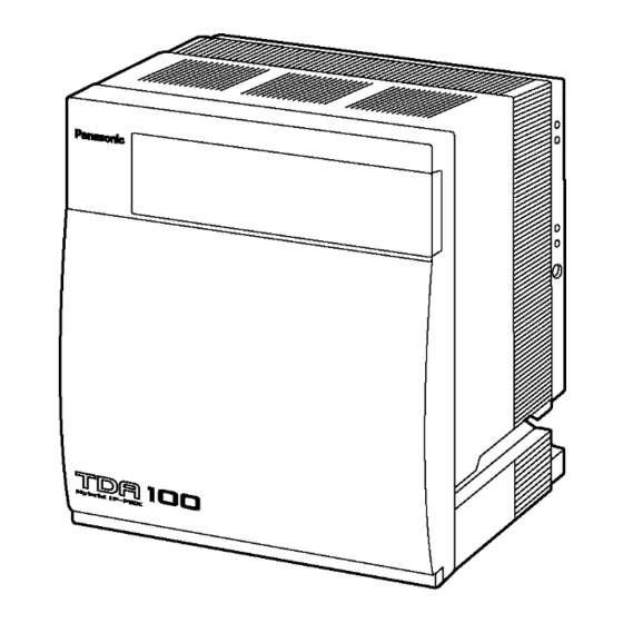
KX-TDA100BX
(for Asia, Middle Near East, South America and Africa)
© 2003 Panasonic Communications Co., Ltd. All
rights
reserved.
distribution is a violation of law.
ORDER NO. KMS0304726C3
Hybrid IP-PBX
Unauthorized
copying
and
Advertisement
Table of Contents

Related Manuals for Panasonic KX-TDA100BX


Summary of Contents for Panasonic KX-TDA100BX
- Page 1 When this mark does appear please read and follow the special instructions described in this manual on the use of PbF and how it might be permissible to use Pb solder during service and repair work. © 2003 Panasonic Communications Co., Ltd. All rights reserved.
-
Page 2: Table Of Contents
KX-TDA100BX CONTENTS Page Page 1 ABOUT LEAD FREE SOLDER (PbF: Pb free) 11.1. INTRUDUCTION 1.1. SUGGESTED PbF SOLDER 11.2. TYPICAL EXAMPLE 1.2. HOW TO RECOGNIZE THAT Pb FREE SOLDER IS 11.3. MPR CARD USED 11.4. ERROR LOG 2 FOR SERVICE TECHNICIANS... -
Page 3: About Lead Free Solder (Pbf: Pb Free)
KX-TDA100BX 1 ABOUT LEAD FREE SOLDER (PbF: Pb free) Note: In the information below, Pb, the symbol for lead in the periodic table of elements, will refer to standard solder or solder that contains lead. We will use PbF when discussing the lead free solder used in our manufacturing process which is made from Tin, (Sn), Silver, (Ag), and Copper, (Cu). -
Page 4: How To Recognize That Pb Free Solder Is Used
KX-TDA100BX 1.2. HOW TO RECOGNIZE THAT Pb FREE SOLDER IS USED Marked PbF (PbF is marked around here) (Component View) PSUP1317ZB RA308 C218 X202 R247 J113 R248 C217 BATALM R243 D407 LED103 CN206 R176 R239 R164 LED101 SDIN R241 R220... -
Page 5: Caution
KX-TDA100BX 3 CAUTION 3.1. NOTE When you note the serial number, write down all of the 11 digits. The serial number may be found on the label affixed to the bottom of the unit. 3.2. SAFETY PRECAUTIONS 1. Before servicing, unplug the power cord to prevent an electric shock. -
Page 6: Specifications
KX-TDA100BX 4 SPECIFICATIONS 4.1. GENERAL DESCRIPTION Control Bus Original bus (16 bit, 8 MHz,10 megabytes per second) Communication Bus H.100 bus conformity (1024 time slot) Switching Non Blocking Distributed Time Switch Power Input PSU-S 100 V AC to 130 V AC/200 V AC to 240 V AC, 1.4 A/0.8 A, 50 Hz/60 Hz... -
Page 7: System Capacity
KX-TDA100BX 4.3. SYSTEM CAPACITY 4.3.1. Maximum Trunk and Extension Cards The following number of trunk and extension cards can be installed in the main unit (Hybrid IP-PBX) for expansion. Card Type KX-TDA100 Trunk Card *1 Extension Card Total *1 One T1, E1, PRI30 and PRI23 card counts as 2 cards. -
Page 8: System Overview
KX-TDA100BX 5 SYSTEM OVERVIEW 5.1. SYSTEM CONFIGURATIONS... -
Page 9: System Components
Blank Slot Cover KX-T30865X Doorphone Available Telephones This main unit (Hybrid IP-PBX) supports all of the Panasonic KX-T7xxx and KX-TD7xxx series: · Digital/Analog proprietary telephones (e.g., KX-T7625, KX-T7630, KX-T7633, KX-T7636) · Portable stations (e.g., KX-TD7690, KX-TD7680) · DSS consoles (e.g., KX-T7640) This main unit (Hybrid IP-PBX) does not support the following telephones: ·... -
Page 10: System Connection Diagram
KX-TDA100BX 5.3. SYSTEM CONNECTION DIAGRAM... - Page 11 KX-TDA100BX *Only 1 Server PC can be connected to the main unit (Hybrid IP-PBX). Two or more Server PCs cannot be used simultaneously.
-
Page 12: Name And Locations
KX-TDA100BX 6 NAME AND LOCATIONS · Null slot: Null slot is not available for any optional service card. LED Type Color Usage and Status Definition RUN Indicator LED1 Green Display of Power Supply & RUN Status (Power/RUN) OFF: Power OFF (inc. in normal resetting) ON: Power ON &... -
Page 13: Disassembly Instructions
KX-TDA100BX 7 DISASSEMBLY INSTRUCTIONS 7.1. DISASSEMBLY INSTRUCTION (MPR CARD) 1. Remove the Lib by sliding it in the direction of arrow 1. 2. This will be removed if the user attached a Pad Lock as shown in a Fig.1. 3. Loosen the Screw. -
Page 14: Disassembly Instruction (Back Board)
KX-TDA100BX 7.2. DISASSEMBLY INSTRUCTION (BACK BOARD) 1. Remove four Screws (A). 2. Remove the Left Side Cover and the Right Side Cover. 3. Remove the Hook. Remove the Top Cover. 4. Remove nine Screws (B). 5. Remove the Back Cover. - Page 15 KX-TDA100BX 6. Remove the RS-232C Connector and LED Connector from Back Board 1. 7. Remove eight Screws (C). 8. Remove Back Board 1. 9. Remove the LED Connector from Back Board 2. 10. Remove the Screw (C). 11. Remove Back Board 2.
-
Page 16: Outline
KX-TDA100BX 8 OUTLINE 8.1. GENERAL DESCRIPTION The control system of the main unit is composed of the main central processing card (MPR card) controlling the entire system and exchanging voice data, the circuit control section (LPR/LC) controlling various telephone lines and the power supply section (POWER). -
Page 17: System Control
KX-TDA100BX 8.2. SYSTEM CONTROL 8.2.1. System Control Block Diagram... - Page 18 KX-TDA100BX 8.2.2. Voice (TDM Highway) Bus Block Diagram...
- Page 19 KX-TDA100BX 8.2.3. Voice Bus Logical Assignment In the line card, the CT_D line number, which is output in accordance with the inserted slot, and the time slot are assigned by software. For the detail of output slot for each card (optional service card), refer to the service manual of the card (optional service card).
-
Page 20: Back Board Signal Connection Diagram
KX-TDA100BX 8.3. BACK BOARD SIGNAL CONNECTION DIAGRAM 8.3.1. CT Bus System Connection Diagram... - Page 21 KX-TDA100BX 8.3.2. EC Bus System Connection Diagram...
- Page 22 KX-TDA100BX 8.3.3. System Control and Analog Signal Connection Diagram 8.3.4. Power Supply System Connection Diagram...
-
Page 23: Mpr Card Circuit Operation
KX-TDA100BX 9 MPR CARD CIRCUIT OPERATION 9.1. MPR CARD 9.1.1. Outline 1) Function · System Control · Circuit Switching (includes gain adjustment function) · Conference Call (3 people x 8 ~ 8 people x 3) · MOH · PAGING · Clock 2) Configuration ·... - Page 24 KX-TDA100BX 9.1.2. Description of Each Part LED (BATALM): Lights when the lithium battery voltage drops below 2.8V. LED (SD ACCES): Lights on when the SD card is being accessed. SD card slot: Mounts the system program SD card. Reset Switch: Press to reset the system.
- Page 25 KX-TDA100BX 9.1.3. Block Diagram...
- Page 26 KX-TDA100BX 9.1.4. Circuit Description 9.1.4.1. Outline of Block Description · CPU block Operates the main unit control. Also operates various controls, generation of select signal, DMA control and serial port control. This contains the built-in clock function. · ASIC block Provides the communication between each optional service card, call control (TSW function), conference call, tone generation and gain control function.
- Page 27 KX-TDA100BX Signal Name Functions nBAT_ALM Battery Alarm Signal: Indicates the declined voltage of lithium battery. (L: Alarm condition) nBREQ Bus Request: Bus request signal Bus Cycle Start: Bus cycle start signal nCASL Lower Byte Address Column Address Strobe: CAS signal for SDRAM...
- Page 28 KX-TDA100BX Signal Name Functions LA[1] -[16] Address bus Lower Byte Select: Indicates Lower byte select signal of SRAM LD[0] -[15] Data Bus LDHW[1] -[0] Down Highway: Data output terminal connected to codec etc. as down data signal of local highway...
- Page 29 KX-TDA100BX Functions as the bus master of EC bus (synchronous bus with 16 bit width, transmission rate max.10Mbps). Communicates with ASIC mounted to each option card via EC bus and controls the option card. Controls CT bus (HW clock 8.192MHz, 8 highway, 128 timeslot) for TSW function.
-
Page 30: Back Board Circuit Operation
KX-TDA100BX clock block power. BAT401, which is a lithium battery for memory backup, is connected to the power supply of IC301, IC302 (SRAM) via D408, D409. IC411 compares BAT401 output voltage to the reference voltage (about 2.8V) and drives LED (BATALM) that indicates dropping of backup voltage. -
Page 31: Troubleshooting Guide
KX-TDA100BX 11 TROUBLESHOOTING GUIDE 11.1. INTRUDUCTION First, check which part of the system is causing the trouble. Follow the flowchart provided below, and replace each unit in turn with a working unit to identify the damaged unit. Even when damaged unit is found out, it may mean that not the cause in the unit but the damaged cause in another unit. -
Page 32: Typical Example
KX-TDA100BX 11.2. TYPICAL EXAMPLE The following items are typical examples when defective occur in main unit. The analysis work first shown in this chapter is done. When you do not correspond to this chapter, or when analysis is not completed, move to the following chapter. -
Page 33: Mpr Card
KX-TDA100BX 11.3. MPR CARD 11.3.1. Startup Run indicator (LED201) - Page 34 KX-TDA100BX SD card access light does not flash The battery alarm indication light turns on...
- Page 35 KX-TDA100BX ALARM indicator flashes · 1 blink and 1 interval · 2 blinks and 1 interval (1 blink is 0.5 sec. ON and 0.5 sec. OFF. 1 interval is 2 sec.) ALARM indicator flashes · 3 blinks and 1 interval ·...
- Page 36 KX-TDA100BX Optional service cards cannot start up...
- Page 37 KX-TDA100BX 11.3.2. Phone Call The call path cannot connect Noise is created...
- Page 38 KX-TDA100BX 11.3.3. Paging No sound (PAGING1) No sound (PAGING2)
- Page 39 KX-TDA100BX Noise is Heard (PAGING1) Noise is Heard (PAGING2)
- Page 40 KX-TDA100BX Sound is small (PAGING1) Sound is small (PAGING2)
- Page 41 KX-TDA100BX 11.3.4. MOH Using No sound is heard (MOH1)
- Page 42 KX-TDA100BX No sound is heard (MOH2)
- Page 43 KX-TDA100BX Sound is small or loud (MOH1) Sound is small or loud (MOH2)
- Page 44 KX-TDA100BX 11.3.5. USB Connection Unable to connect...
- Page 45 KX-TDA100BX Connection error occurs...
- Page 46 KX-TDA100BX 11.3.6. RS-232C Connection Unable to connect...
- Page 47 KX-TDA100BX Connecting speed is slowly...
- Page 48 KX-TDA100BX 11.3.7. SD Card I/F Unable to save the system data...
- Page 49 KX-TDA100BX 11.3.8. Other The clock data is deleted (unset table)
-
Page 50: Error Log
KX-TDA100BX 11.4. ERROR LOG When a major system error occurs in the main unit (Hybrid IP-PBX), the ALARM indicator on the front of the cabinet turns on red, and the system logs the error information. 11.4.1. Error Log Display Format... - Page 51 KX-TDA100BX 11.4.2. List of Errors and Solutions The tables below list the errors and their solutions. When an error whose error code is indicated with "*" occurs in the main unit (Hybrid IP-PBX), the ALARM indicator on the front of the cabinet turns on red, and the system logs the error information.
- Page 52 KX-TDA100BX Error Code Error Message PROBABLE CAUSE SOLUTION · Optional service card malfunction: · See if the corresponding optional service card is installed PT I/F error DHLC, DLC properly · Software error due to external · Pull out and re-insert the corresponding optional service...
- Page 53 KX-TDA100BX Error Code Error Message PROBABLE CAUSE SOLUTION · Not enough memory space · Delete the files whose file names start with "$" from SD 022* Not enough free space on SD card available to save the system data, Memory Card or to upload system files from the ·...
- Page 54 KX-TDA100BX Error Code Error Message PROBABLE CAUSE SOLUTION · Optional service card malfunction: · See if the corresponding optional service card is installed LPR alive check error DHLC, DLC, CSIF, T1, PRI, OPB3, properly MPR-LPR CTI-LINK, E&M, IP-GW communication error ·...
-
Page 55: Diagnosis
KX-TDA100BX 12 DIAGNOSIS 12.1. DIAGNOSIS FEATURES Card Test and Pair Port Test is in Diagnosis Features. 12.1.1. Card Test Card Test -SUMMARY Description Diagnose all kind of Cards. Parallel of Diagnose item of Card Tests and every Cards DHLC SLC8/L... - Page 56 KX-TDA100BX 12.1.1.2. Card CT Bus Diagnosis Diagnose CT bus by Loop back test to use CT bus DHLC SLC8/L MSLC/ CS-INF LCOT OPB3 E&M CTI- SLC8 SLC16 LINK Object of Card Diagnosis result Card CT bus diagnosis OK Card CT bus diagnosis NG 12.1.1.3.
- Page 57 KX-TDA100BX 12.1.1.6. DSP DTMF Receiver Diagnosis Diagnose DTMF receiver of DSP in the Card to use DTMF generator of DSP DHLC SLC8/L MSLC/ CS-INF LCOT OPB3 E&M CTI- SLC8 SLC16 LINK Object of Card Diagnosis point Time slot Time slot test...
- Page 58 KX-TDA100BX 12.1.1.10. Super Frame Synchronization Diagnosis Diagnose Super frame synchronization feature of CS-INF DHLC SLC8/L MSLC/ CS-INF LCOT OPB3 E&M CTI- SLC8 SLC16 LINK Object of Card Diagnosis point DECT DECT super frame synchronization test SS super frame synchronization test...
-
Page 59: Diagnosis Test
KX-TDA100BX 12.2. DIAGNOSIS TEST 1. Click [Diagnosis] of [Utility]. - Page 60 KX-TDA100BX 2. Pair Port Test operation Select card for Test. 3. Click [Pair Port Test].
- Page 61 KX-TDA100BX 4. Click [OK]. 5. Click [Cancel].
- Page 62 KX-TDA100BX 6. Card Test operation Select card for Test. 7. Click [Card Test].
- Page 63 KX-TDA100BX 8. Click [OK]. 9. Click [Cancel].
-
Page 64: Ic Data
KX-TDA100BX 13 IC DATA 13.1. IC101 Pin No. Pin Name Description Clock mode setting Clock mode setting Vcc-TRC*1 Power for RTC XTAL2 Crystal oscillator terminal for built-in RTC EXTAL2 Crystal oscillator terminal for built-in RTC (*6) Vcc-TRC*1 Power for RTC... - Page 65 KX-TDA100BX Pin No. Pin Name Description Power supply (*3) Power supply (*3) D18/PTA[2] Data bus/I/O port A D17/PTA[1] Data bus/I/O port A D16/PTA[0] Data bus/I/O port A VssQ Power for I/O (0V) Data bus VccQ Power for I/O (3.3V) Data bus...
- Page 66 KX-TDA100BX Pin No. Pin Name Description WE3/DQMUU/ICIOW O/I/O D31-D24 select signal/DOM (SDRAM) /PCMCIA I/O write/I/O port K R/PTK[7] RD/WR Read/Write AUDSYNC/PTE[7] O/I/O AUD synchronization/I/O port E VssQ Power for I/O (0V) CS0/MCS[0] Chip select 0/mask ROM chip select 0 VccQ Power for I/O (3.3V)
- Page 67 KX-TDA100BX Pin No. Pin Name Description Power supply (*3) XTAL Clock oscillator terminal EXTAL External clock/crystal oscillator terminal STATUS0/PTJ[6] O/I/O Processor status STATUS0/PTJ[7] O/I/O Processor status TCLK/PTH[7] Clock I/O for TMU or RTC/I/O port J IRQOUT Interrupt request notification VssQ...
-
Page 68: Terminal Guide Of Ics, Transistors And Diodes
KX-TDA100BX 14 TERMINAL GUIDE OF ICS, TRANSISTORS AND DIODES... -
Page 69: How To Replace A Flat Package Ic
KX-TDA100BX 15 HOW TO REPLACE A FLAT PACKAGE IC 15.1. PREPARATION 15.3. REMOVING SOLDER FROM BETWEEN PINS · PbF (: Pb free) Solder · Soldering Iron 1. Add a small amount of solder to the bridged pins. Tip Temperature of 700°F ± 20°F (370°C ± 10°C) 2. -
Page 70: Cabinet And Electrical Parts Location
KX-TDA100BX 16 CABINET AND ELECTRICAL PARTS LOCATION... -
Page 71: Extension Boards For Servicing
KX-TDA100BX 16.1. EXTENSION BOARDS FOR SERVICING... -
Page 72: Accessories And Packing Materials
KX-TDA100BX 17 ACCESSORIES AND PACKING MATERIALS... -
Page 73: Replacement Parts List
KX-TDA100BX 18 REPLACEMENT PARTS LIST Note: Ref. Part No. Part Name & Description Remarks 1. RTL (Retention Time Limited) PSMH1205Z CHASSIS, LED The marking (RTL) indicates that the Retention Time is PSHD1091Z BOLT WITH NUT limited for this item. PSKV1016Z1... -
Page 74: Mpr Card Parts
KX-TDA100BX Ref. Part No. Part Name & Description Remarks 18.3. MPR CARD PARTS D409 MA728 DIODE(SI) Ref. Part No. Part Name & Description Remarks DA401 MA143 DIODE(SI) PCB1 PSWP1DA100BX MPR CARD ASS´Y (RTL) DA402 MA143 DIODE(SI) (ICS) LED101 PSVD1VGCT IC101... - Page 75 KX-TDA100BX Ref. Part No. Part Name & Description Remarks Ref. Part No. Part Name & Description Remarks RA306 D1HA1038A005 RESISTOR ARRAY C174 ECUV1C104ZFV RA307 D1HA1038A005 RESISTOR ARRAY RA308 D1HA1038A005 RESISTOR ARRAY C201 ECUV1H220JCV RA309 D1HA1038A005 RESISTOR ARRAY C202 PQCUV1A225ZF C203...
- Page 76 KX-TDA100BX Ref. Part No. Part Name & Description Remarks Ref. Part No. Part Name & Description Remarks R137 ERJ3GEYJ103 C430 ECUV1H153KBV 0.015 R138 ERJ3GEYJ103 C431 ECUV1H153KBV 0.015 R139 ERJ3GEYJ103 C433 ECUV1C104ZFV C435 ECUV1A105ZFV R140 ERJ3GEYJ330 C436 ECUV1A105ZFV R142 ERJ3GEYJ330 C437 ECUV1H333KBV 0.033...
- Page 77 KX-TDA100BX Ref. Part No. Part Name & Description Remarks Ref. Part No. Part Name & Description Remarks R241 ERJ3GEYJ473 R455 ERJ3GEYJ223 R242 ERJ3GEYJ473 R456 ERJ3GEYJ223 R243 ERJ3GEYJ104 100k R457 ERJ3GEYJ223 R244 ERJ3GEYJ472 4.7k R458 ERJ3GEYJ472 4.7k R245 ERJ3GEYJ473 R459 ERJ3GEYJ472 4.7k...
- Page 78 KX-TDA100BX Ref. Part No. Part Name & Description Remarks Ref. Part No. Part Name & Description Remarks J115 PQ4R18XJ000 L115 ERJ3GEY0R00 J116 PQ4R18XJ000 L116 ERJ3GEY0R00 J121 ERJ3GEY0R00 L117 ERJ3GEY0R00 J123 ERJ3GEY0R00 L118 ERJ3GEY0R00 J126 ERJ3GEY0R00 L119 ERJ3GEY0R00 J129 ERJ3GEY0R00 J130...
-
Page 79: Back/Led Board Parts
KX-TDA100BX Ref. Part No. Part Name & Description Remarks Ref. Part No. Part Name & Description Remarks L186 PFVF1A471SG CERAMIC FILTER X101 PSVCC0025GT CRYSTAL OSCILLATOR L187 PFVF1A471SG CERAMIC FILTER X102 PSVCC0019CT CRYSTAL OSCILLATOR L189 PFVF1B470SB CERAMIC FILTER X103 H1B1635B0016 CRYSTAL OSCILLATOR... -
Page 80: Fixtures And Tools
KX-TDA100BX Ref. Part No. Part Name & Description Remarks R151 ERJ3GEYJ103 R152 ERJ3GEYJ103 R153 ERJ3GEYJ103 R154 ERJ3GEYJ103 R155 ERJ3GEYJ103 R156 ERJ3GEYJ103 R157 ERJ3GEYJ103 R165 ERJ3GEYJ103 R166 ERJ3GEYJ103 R167 ERJ3GEYJ103 R168 ERJ3GEYJ103 R169 ERJ3GEYJ103 R170 ERJ3GEYJ103 R177 ERJ3GEYJ103 R178 ERJ3GEYJ103 R179... -
Page 81: For The Schematic Diagram
KX-TDA100BX 19 FOR THE SCHEMATIC DIAGRAM Note: 1. DC voltage measurements are taken with an oscilloscope or a tester with a ground. 2. The schematic diagrams and circuit board may be modified at any time with the development of new technology. -
Page 82: Schematic Diagram
KX-TDA100BX A[0-25] A[0-25] D[0-31] LD[0-15] IC127 A[25] +3.3V +3.3V TP131 TP266 L122 TP185 TP349 TP375 IC125 IC125 A[23] D[31] D31/PTB(7) A[25] TP2027 L123 TP132 TP186 TP267 TP350 TP376 nBACK D[30] A[24] D30/PTB(6) TP1008 TP2026 LD[15] TP133 IC101 TP268 L124 TP187... - Page 83 KX-TDA100BX CN103 L178 NC +3.3V_ASIC +3.3V +3.3V (+15VPT) FIL108 IC102 (+15VPT) TP504 R144 TP467 EC_CLK A[20] EC_CLK 111 EC_CLK ADD[20] RA133 +3.3V C175 R161 R172 (+40V) TP468 R192 A[19] EC_STOP 109 EC_nSTOP ADD[19] A[18] EC_TRDY 108 TP469 R193 EC_nTRDY N.C.
- Page 84 KX-TDA100BX...
- Page 85 KX-TDA100BX...
- Page 86 KX-TDA100BX...
-
Page 87: Back/Led Board
KX-TDA100BX... - Page 88 KX-TDA100BX...
- Page 89 KX-TDA100BX...
-
Page 90: Waveform
KX-TDA100BX... - Page 91 KX-TDA100BX...
-
Page 92: Printed Circuit Board
KX-TDA100BX... - Page 93 KX-TDA100BX C308 J116 C311 C310 C219 C309 C312 C220 C313 L303 FIL304 C210 R412 FIL303 L304 J411 L404 IP402 FIL302 C406 R410 D405 R409 R411 D402 R105 RA206 C403 C451 IC412 C452 C303 C305 IC123 IC124 R144 C315 C317 R526...
-
Page 94: Back/Led Board
KX-TDA100BX... - Page 95 KX-TDA100BX +15VPT +40V Power GND EC_AD[11]...
- Page 96 KX-TDA100BX KXTDA100BX...