Table of Contents
Advertisement
FILE NO. 810-201082GR
SERVICE MANUAL
Blu-ray Disc Player
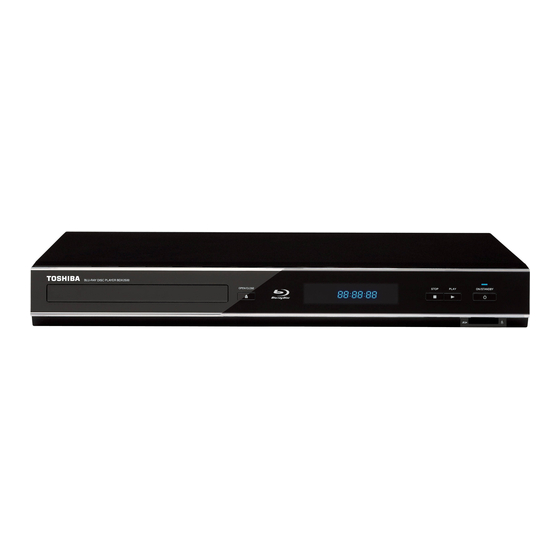
BDX2500KU
The above model is classified as a green product (*1), as indicated by the underlined serial number.
This Service Manual describes replacement parts for the green product. When repairing this green
product, use the part(s) described in this manual and lead-free solder (*2).
For (*1) and (*2), see the next page.
Jun. 2010 GREEN
Advertisement
Table of Contents

Related Manuals for Toshiba BDX2500KU


Summary of Contents for Toshiba BDX2500KU
- Page 1 FILE NO. 810-201082GR SERVICE MANUAL Blu-ray Disc Player BDX2500KU The above model is classified as a green product (*1), as indicated by the underlined serial number. This Service Manual describes replacement parts for the green product. When repairing this green product, use the part(s) described in this manual and lead-free solder (*2).
- Page 2 (*1) GREEN PRODUCT PROCUREMENT The EC is actively promoting the WEEE & RoHS Directives that define standards for recycling and reuse of Waste Electrical and Electronic Equipment and for the Restriction of the use of certain Hazardous Substances. From July 1, 2006, the RoHS Directive will prohibit any marketing of new products containing the restricted substances.
-
Page 3: Table Of Contents
CONTENTS 1. PRINTED WIRING BOARD AND SCHEMATIC DIAGRAM Printed Wiring Board and Schematic Diagram ……………………………………………………..……..……... 1-1 2. BLOCK DIAGRAM …………………………………………………………………………………………. 2-1 3. CIRCUIT DIAGRAMS Power Supply Circuit Diagram …………………….……………………………………………….…..….……..3-1 Front Display Circuit Diagram …………………….……………………………………………….…..………..3-2 SD Card Connector Circuit Diagram ………………………………………………………………………………. 3-3 7.1 CH Audio Output Circuit Diagram …………………………………………………………………………….. -
Page 4: Printed Wiring Board And Schematic Diagram
PRINTED WIRING BOARD AND SCHEMATIC DIAGRAM Mechanism FFC CABLE 45 PINS L=280mm FCS2+ FCS2- TRK+ FCS1+ TRK- FCS1- AUDIO FFC CABLE 15 PINS L=150mm PWR_ON0 DGND AMCLK NC(GND) DNGD I2S_BLK_OUT DGND CN9201 CN9301 AOSDATA1 I2S_LRWS_OUT AOSDATA2 SW3(BD) AOSDATA3 CN4501 AOSDATA4 SWB2(BD) +12V SWB1(BD) -
Page 5: Block Diagram
Block Diagram KEY & R/C VFD DISPLAY SD CARD VFD DRIVER NAND FLASH DSP + MCU BDVD LOADER BCM7630 BDVD DRIVER BDVD MECHANIS 7.1 CH AUDIO OUTPUT AUDIO & VIDEO OUTPUT DC/DC REGULATOR AC/DC RECTIFIER FOR SYSTEM POWER SUPPLY AC120V... -
Page 6: Circuit Diagrams
CIRCUIT DIAGRAMS Power Supply Circuit Diagram HER203 BEAD EEL22001W 220UF/ 25V 220UF/ 25V 5. 8V 2200 PF/ 250VAC D13,D16 1N4007 1500 UF/ 10V 47UF/ 200V DR8*10,10U 1N5822 T1A/ 250V 1N4007 UU9. 8001L 0. 22u/ 275VAC 1000 UF/ 10V THR1 1N4007 SCK-054 222/ 630V EEL22001W... -
Page 7: Front Display Circuit Diagram
Front Display Circuit Diagram C106 A100 115-220901W100 HD DVD HNV-09SS73T HDMI TITLE 1080ip 720P 567ip 480ip For POWER indication R114 680R 680R USE FOR BDX2700KU For Blue-Ray LOG D120 D103 BLUE BLUE Q101 3DA8050M L102 R109 1K Q104 MMZ1608S601CTAH0 3DA8050M C108 10uF/50V C105... - Page 8 SD Card Connect Circuit Diagram SD_VDD 100n DGND CON1 FB7 0R SD_D2 FB6 0R SD_D3 DAT3 FB5 0R SD_CMD SD_PWR VSS1 SD_GND FB4 0R SD_CLK SD_GND VSS2 FB3 0R SD_D0 DAT0 FB2 0R SD_D1 DAT1 FB1 0R SD_CD DAT2 SD_WP CARD DETECT FB8 0R SD_GND...
-
Page 9: 7.1 Ch Audio Output Circuit Diagram
7.1 CH Audio Output Circuit Diagram IC9302 CONT C9310 1uF/16V TK11150CSCL-G C9305 0.01uF C9327 1uF/16V C9301 C9306 R9322 IC9301 R9323 22R VSS2 C9311 C9328 C9336 C9323 CVDD 0.1uF 0.001uF 100pF 47uF/10V R9302 MCLK R9303 C9319 C9329 C9312 BICK VSS1 0.001uF 47uF/10V 0.1uF R9304... -
Page 10: Audio Output Circuit Diagram
Audio Output Circuit Diagram IC9001 TK11150CSCL-G IC9002 AK4424AET-E2... -
Page 11: Video Output Circuit Diagram
Video Output Circuit Diagram BCM7630BKFEBG Video DAC IC4001... -
Page 12: Hdmi Output Circuit Diagram
HDMI Output Circuit Diagram BCM7630BKFEBG HDMI IC4001... -
Page 13: Ether, Usb Circuit Diagram
Ether, USB Circuit Diagram BCM7630BKFEGB ETHERNET IC4001 REAR USB JACK BCM7630BKFEBG IC5001 BD6538G-TR IC4001 TO Wifi... -
Page 14: Gpio Circuit Diagram
GPIO Circuit Diagram Boot Strap Options BCM7630BKFEGG IC7002 XC6209F332PR FRONT DDR Strap GPIOs IC4001 SD IO... -
Page 15: Nand, Clock, Test & Reset Circuit Diagram
Nand, Clock, Test & Reset Circuit Diagram BCM7630BKFEBG IC5101 BCM7630BKFEBG EJTAG/BBS IC4001 K9G2G08U0A FLASH IC4001 DEBUG BCM7630BKFEBG Clocks IC4001 IC4201 BD46302G BCM7630BKFEBG BCM7630BKFEBG Reset Reset IC4001 IC4001 3-10... -
Page 16: Ddr3 Circuit Diagram
DDR3 Circuit Diagram BCM7630BKFEBG DDR3 IC4001 3-11... -
Page 17: Ddr3 Parts Circuit Diagram
DDR3 Parts Circuit Diagram IC5202 Ic5203 IC5201 K4B1G0846E-HCH9 K4B1G0846E-HCH9 K4B1G1646E-HCH9 3-12... -
Page 18: Motor Servo & Driver Circuit Diagram
Motor Servo & Driver Circuit Diagram BCM7630BKFEBG IC4402 R2A30209SP_W02Z IC4403 LB1848M-TE-R-E Optical Front End IC4001 3-13... -
Page 19: Motor & Servo Connect Circuit Diagram
Motor & Servo Connect Circuit Diagram LD1117SC-R IC4501 3-14... -
Page 20: Main Power Circuit Diagram
Main Power Circuit Diagram BCM7630BKFEBG IC8001 MP2307DN IC8002 MP2307DN 1.5V for DDR3 IC8003 Powers AOZ1014DI IC4001 3-15... -
Page 21: Pc Boards
PC BOARDS Power Supply PC Board Loader Relay PC Board Power Supply PC Board (Top Side) SD Card PC Board Power Supply PC Board (Bottom Side) -
Page 22: Audio Pc Board
Audio PC Board Audio PC Board (Top Side) Audio PC Board (Bottom Side) Front PC Board Front PC Board (Top Side) Front PC Board (Bottom Side) -
Page 23: Main Pc Board
Main PC Board Main PC Board (Top Side) - Page 24 Main PC Board Main PC Board (Bottom Side)
-
Page 25: Ic Pins Description And Block Diagrams
IC PINS DESCRIPTION AND IC BLOCK DIAGRAMS IC5201 NT5CB64M16AP/NT5CB128M8AN/NT5CB256M4AN - 1 Input / Output Functional description Function Symbol Type Clock: CK and CK are differential clock inputs. All address and control input signals CK,CK Input are sampled on the crossing of the positive edge of CK and negative edge of CK. Clock Enable: CKE high activates, and CKE low deactivates, intermal clock signals and device input buffers and output drivers. - Page 26 IC5201 NT5CB64M16AP/NT5CB128M8AN/NT5CB256M4AN - 2 Input / Output Functional description Function Symbol Type Active Low Asynchronous Reset: Reset is avtive when RESET# is LOW, and inactive when RESET# is HIGH. RESET# must be HIGH during normal operation. RESET Input RESET# is a CMOS rail to rail signal wigh DC high and low at 80% and 20% of VDD, I,e, 1.20V for DC high and 0.30V.
- Page 27 IC5202, IC5203 NT5CB256M4CN/NT5CB128M8CN - 1 Input / Output Functional description Function Symbol Type Clock: CK and CK are differential clock inputs. All address and control input signals CK,CK Input are sampled on the crossing of the positive edge of CK and negative edge of CK. Input Clock Enable: CKE high activates, and CKE low deactivates,intermal clock signals and device input buffers and output drivers.
- Page 28 IC5202, IC5203 NT5CB256M4CN/NT5CB128M8CN - 2 Input / Output Functional description Function Symbol Type No Connect: No internal electrical connection is present. VDDQ Supply DQ Power Supply: 1.5V ± 0.075V Supply Power Supply: 1.5V ± 0.075V VSSQ Supply DQ Ground Supply Ground VREFCA Supply...
- Page 29 IC101 PT6315 SG1/KS1 SG2/KS2 SG3/KS3 SG4/KS4 SG5/KS5 Control SG6/KS6 SG7/KS7 Serial DOUT Data SG8/KS8 Display Memory Interface Segment SG9/KS9 (24 bits x 16 Words) Driver/ SG10/KS10 SG11/KS11 Grid SG12/KS12 Driver/ SG13/KS13 SG14/KS14 Timing Generator SG15/KS15 Key Scan Output SG18/KS18 SG17/GR12 SG18/GR11 SG19/GR10 SG20/GR9...
- Page 30 IC2301, IC9001, IC9302 TK11150CSCL Vout Over Heat & Over Current Control Protection Circuit Bandgap Reference Vcont IC4401 NJM2125F OUTPUT +INPUT -INPUT...
- Page 31 IC3001 BH76071FJ CLAMP CVBS_IN CVBS_OUT 8.75MHz MUTE1 VREF 13.5MHz CLAMP PY_IN PY_OUT 30MHz MUTE2 BIAS PB_IN BIAS PR_IN 13.5MHz PB_OUT 30MHz MUTE2 MUTE1 13.5MHz PR_OUT 30MHz MUTE2 MUTE2 LPF_SEL IC4101 TC7SH14FU IC4201 BD45482G IN A Counter OUT Y Vref...
- Page 32 IC4501 LD1117STR Thermal Limit Current Limit Substrate GND (fixed output) ADJ. (adjustable output) IC8003 AOZ1014DI UVOL 5V LDO & Internal +5v REGULATOR ISEN REFERENCE & SOFTSTART BIAS ILIMIT 0.8V CONTROL EAMP COMP LOGIC COMP 500kHz OSCILLATOR AGND PGND...
- Page 33 IC5101 TC58NVG1S3ETA Vcc Vss Status register Address register Column buffer I/O1 Column decoder Control circuit I/O8 Command register Data register Sense amp Memory cell array Logic control Control circuit RY/BY HV generator RY/BY IC8001, IC8002 MP2307DN CURRENT SENSE AMPLIFIER 1.1V RAMP OSCILLATOR 100/340kHz...
- Page 34 IC4402 R2A30209SP For LOADING 4.5-5.5V For/ACT1/ACT2/ACT3 7-13.2V 4.5-5.5V Current gain For SPINDLE 3A/V 10.8-13.2V 0.6A/V H Bridge Voltage gain Voltage gain Voltage gain SWICHING CIRCUIT Commutation Frequency 150KHz Current gain Current gain ACGS 0.88 A/V 0.88 A/V Gain Select Commutation SPGS (SPM and ACT) Frequency...
- Page 35 IC5001 BD6538G IC9002, IC9301, IC9303, IC9305 AK4424AET MCLK Delay Counter De-emphasls Clock SMUTE Control Control Divider Interface Charge UVLO VSS1 pump ∑ AOUTL LRCK Interpolator Modulator Audio BICK Data Interface ∑ SDTI AOUTR Interpolator Modulator Charge IC4403 LB1848M Pump CVDD 80kW 80kW OUT1...
-
Page 36: Parts List
AH700759 SUBBD2500KUSD SD CARD PCB ASS'Y MODEL BDX2500KU1 AH700760 SUBBDX2500FNT FRONT PCB MODULE FOR BDX2500KU14 AH700761 038-002001W000 POWER SUPPLY PCB MODULE FOR BDX2500KU TPS-020U01 AH700762 600-BD2520W001 TOP COVER BD25-20, T=0.4mm E.G. C20/20E CR-FREE, w/CSM-0560 (DARK BLACK 2010) SPY AH700763 SUBBDX2500KUMN MAIN PCB ASS'Y OF MODEL BDX2500KU1... -
Page 37: Exploded View
EXPLODED VIEW... -
Page 38: Specifications
Specifications General Signal system NTSC color Power requirements 120 V AC, 60 Hz Power consumption 23 W Dimensions (width x height x depth) 430 x 58.5 x 209.7 mm Weight 1.7 kg Operating temperature 41°F (5°C) to 95°F (35°C) Operating humidity Less than 80% (no condensation) Terminals Video output... -
Page 39: Remote Control Se-R0378 Code Table
REMOTE CONTROL SE-R0378 CODE TABLE NEC format -- (2nd frame and subsequent frames are continuous pulses when key is pressed down and hold). Customer code -- 45BA Key No. Key Name FORMAT Custom Code(Hex) Data Code(Hex) OPEN/CLOSE 45B5 ON/STANDBY 45B5 INFO 45B5 SETTING... -
Page 40: Firmware Upgrade Procedure
6. Press “left arrow key” on remote control to EN T Firmware Upgrade select “OK”. Procedure 7. Press ENT/ENTER on remote control. Do not power off the unit from For Engineering Evaluation Only now for at least 5 minutes until the firmware upgrade is completed. -
Page 41: Trouble Shooting Chart
Trouble shooting chart 11-1 7.1 CH Audio no output. No 7.1 CH Audio output Check whether there is correct contact between CN9301 and Correct connection. CN9201. Check E6A(+5.8V) voltage Check Power board and Main on 7.1 CH Audio board and board or replace them. - Page 42 Trouble shooting chart 11-2 LAN port no output. LAN no output. Check whether IC4001 Pin W21, W22,V22,V21,arrive the J2001 Correct connection. pin4,5,1,2. Check whether bad solder Replace J2001. exists on J2001. Replace IC4001 or Main board.
- Page 43 Trouble shooting chart 11-3 Spindle motor does not move. Motor no move Check the FFC connection Correct connection. between 45P and the loader. Check whether "RFA5V" Check the RFA5V power supply (+5V) voltage is normal. or replace Main PCB. Check whether laser voltage Check/Replace Q4504,Q4506 (2.3V for DVD &...
- Page 44 Trouble shooting chart 11-4 The power can not be on or off. The power can't be on or off. Check the power supply Repair the Power board on the Power board is normal. or replace Power PCB. Check if the CN2 on the Power board to CN8001 on the Check/Correct connection.
- Page 45 Trouble shooting chart 11-5 All output voltages on the Power board is 0V or deviated. All output voltages on the Power board is 0V or deviated. Replace FU1 or replace Power PCB. Check whether FU1 is blown. Check whether there is Replace C8 if D17, D19, D20,D21 are 130V on C8.
- Page 46 Trouble shooting chart 11-6 Disc cannot be read. Disc cannot be read. Check the FFC connection Check the loaded circuit. between 45P and the loader. 1.Check voltage on pin C11,C10,B10 of IC4001 varies between 0 and 3.3V : Check whether there is laser 3.3V for CD voltage (2.3V for DVD and 1.9V 0V for DVD...
- Page 47 Trouble shooting chart 11-7 No display on LED, and buttons do not work. No display on LED, and buttons do not work. Check whether there is Correct connection. correct contact between CN7001 and CN100. Fix power supply board top a power Check VCC(+3.3V) voltage on supply for should electric circuit or the Power and Front board.
- Page 48 Trouble shooting chart 11-8 Abnormal color of video picture. Abnormal color of video picture. Check X4201.C4203 and C4204 Replace Main PCB. whether the 27MHz output signal. Check other of power supply Check whether the 3.3V, 1.2V electric circuit or replace Main and 1.5V power supply voltages PCB.
- Page 49 Trouble shooting chart 11-9 Remote reception is insensitive or fails. Remote reception is insensitive or fails. Check if the remote control Check battery. works properly. Check if the power supply Check R103 or replace Front PCB. voltage to the remote sensor is normal.
- Page 50 Trouble shooting chart 11-10 No video picture, no sound. No video picture, no sound. Check whether all the voltages Check the loaded circuit. from the power board to the Decoder board are normal. CVBS (R1 point) waveform Check if the reset circuit consisting of IC4201,C4205,C4206 and R4206 Change IC4201,C4205,C4206...
- Page 51 Trouble shooting chart 11-11 HDMI Failure. HDMI Failure. Select HDMI output. Is "Video out" Set from setup. selected HDMI? Confirm TV side is selected connected HDMI port. Re-connect HDMI cable. Poor connection of HDMI terminal? DVD and TV both side. Is TV support set It changes to the resolution which TV is supporting.
- Page 52 1-1, SHIBAURA 1-CHOME, MINATO- KU, TOKYO 105-8001, JAPAN...