
Related Manuals for LG GCC-4241N


Summary of Contents for LG GCC-4241N
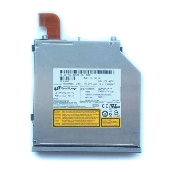
- Page 1 Slim CD-RW/DVD-ROM Drive S E RVICE MANUAL MODEL: GCC-4241N P/NO : 3828HS1043A August, 2003 Printed in Korea MODEL : GCC-4241N...
-
Page 2: Table Of Contents
TABLE OF CONTENTS INTRODUCTION..............................3 FEATURES ................................3 SPECIFICATIONS .............................4~6 DISASSEMBLY ..............................7 1. CABINET ...............................7 2. MAIN CIRCUIT BOARD..........................7 3. FRONT PANEL ..............................7 4. BASE PICK-UP ..............................7 EXPLODED VIEW ..............................8 MECHANICAL REPLACEMENT PARTS LIST....................9~10 GLOSSARY .................................11 THE DIFFERENCES OF CD-R/CD-RW DISCS AND GENERAL CD-ROM ..........12~18 1. -
Page 3: Introduction
INTRODUCTION This service manual provides a variety of service or compatible slim notebook computer. It can write information. as much as 700 Mbytes of digital data into CD-R It contains the mechanical structure of the CD-RW disc, and can read as much as 700 Mbytes of digital /DVD-ROM Drive and the electronic circuits in data stored in a CD-ROM, CD-R and CD-RW disc. -
Page 4: Specifications
SPECIFICATIONS 1. SYSTEM REQUIREMENTS -CPU: IBM Compatible Pentium750MHZ (or faster) -64MB Memory or greater 2. SUPPORTING OPERATING SYSTEM 1) Read 2) Write 3) Recording tool • DOS 3.0 or Higher • Window 98 Second Edition • Easy CD Creator • Windows 95 OSR 2.1 •... - Page 5 4. DRIVE PERFORMANCE 1) Read/Write & Rotational Speed(TBD) <Read> DVD-ROM Single Layer 3.3x~8x(CAV): Approx. 4,710r/min Dual Layer 3.3x~8x (CAV) : Approx. 5,180 r/min CSS Title 1.7x~4x (CAV): Approx. 2,600 r/min DVD-R 3.95GB 1.7x~4x (CAV): Approx. 2,600 r/min 4.7GB 1.7x~4x (CAV) : Approx.
- Page 6 5. Quality and Reliability 1) MTBF.............. 80,000 Power On Hours (POH) Assumption : Use in a normal office environment -POH per year 3,000 - ON/OFF cycles per year 12000 -Operating duty cycle 10% of Power on time (Seek : 10% of operating time) 2) Tray Cycle Test ..........
-
Page 7: Disassembly
DISASSEMBLY 1. CABINET 3. FRONT PANEL A. Release 3 screws (A). A. Remove the Front Panel.(The Front Panel is a snap on B. Lift up the Cabinet in the direction of arrow (1). type.) (See Fig.1) B. At this time, be careful not to damage the 3 hooks (a) of the it. -
Page 8: Exploded View
EXPLODED VIEW PBM00(MAIN C.B.A) ˚... -
Page 9: Glossary
GLOSSARY ATIP Absolute Time in Pre-groove. With an additional modulation of the “Wobble”, the “Groove” contains a time code information. Wobble The pre-groove in the Disc is not a perfect spiral but is wobbled. With : – A typical amplitude of 30 nm –... -
Page 10: The Differences Of Cd-R/Cd-Rw Discs And General Cd-Rom
The differences of CD-R/CD-RW discs and General CD-ROM 1. Recording Layer Recordable CD has a wobbled pre-groove on the surface of disc for laser beam to follow track. Track pitch(p) a=30nm Read-only Disc CD-ROM (READ-ONLY DISC) Radial Direction Radial Error Signal 0.4~0.5 um Groove Land... -
Page 11: Disc Materials
3. Disc Materials 1) CD-ROM disc • It is composed of Silver _ colored aluminum plate and Reflective layer. • Groove (Pit) of aluminum plate make a track. • Laser wavelength : 780 nm, Laser Power (Read): 0.5mW • Signal is detected by the difference of reflective beam intensity between “pit”... -
Page 12: Reading Process Of Optical Disc
3) CD-RW Disc Label Printing Protective Layer Dielectric Layer(TL) Reflective Layer Dielectric Layer(UL) Substrate (Polycarbonate) Groove Laser Beam • It is composed of polycarbonate layer, alloy(silver, arsenic) layer, aluminum reflectivity layer, protective layer. • An crystalized alloy layer is transformed into noncrystalized by the laser heat. Therefore, writing and reading is enabled by the difference of reflectivity. -
Page 13: Writing Process Of Cd-R Disc
5. Writing Process of CD-R Disc Incident (Write) Laser Power (Read) (Read) Laser Spot a b c d e f Position (Time) Laser Below "ORP"– Mark Too Short Spot Reflected At Optimum Record Power ("ORP") Light Signal Above "ORP" – Mark Too Long Recorded Mark Time... -
Page 14: Organization Of The Pca, Pma And Lead-In Area
7. Organization of the PCA, PMA and Lead-in Area 1) Layout of CD-ROM disc Disc Center Diameter 120 mm Diameter 46 mm Diameter 15 mm Center hole Clamping and Label Area Information Area Read Only Disc Lead-in Area Program Area Lead-out Area 2) Layout of CD-R/RW disc Disc Center... -
Page 15: Function Of Pca And Pma Area
8. Function of PCA and PMA area 1) PCA (Power Calibration Area) • PCA area is used to determine the correct Laser Power for a disc. – Method 1 : PCA area is divided by a track. – Method 2 : The previous Calibration value is referred. –... -
Page 16: Writing Process Of Disc
2) ROPC (Running Optimum Power Control) • Variable primary factor of Optimum Power – Change of Power sensitivity on the Disc. (limited to 0.05 *Po) – Wavelength shift of the laser diode due to the operating temperature change. – Change of the Spot aberration due to the Disc skew, Substrate thickness, Defocus. -
Page 17: Description Of Data Processing
DESCRIPTION OF DATA PROCESSING 1. Data Processing Flow... -
Page 18: Copy Protection And Regional Code Management Block
2. Copy Protection and Regional Code Management Block Block Diagram Change the "KEY" HOST DVD PLAYER MN103S63G (EMPEG2 B/D) Scrambled MPEG Data KEY Management Control Brief Process 1. Regional Code for DVD Disc – DVD-ROM drive transfers the regional code of the control data to host by the command of host, the DVD player of host reads the regional code, and plays title in the case of allowed regional code only. -
Page 19: About Prevention The Dvd-Rom From To Be Copy
3. About Prevention the DVD-ROM from to be copy A data is able to encode and record in the disc, if a copyright holder wants to prevent the disc from copying. In case of a disc enhanced movie of 3 titles..DISC KEY (2048 Bytes) is used to encode the whole contents in the disc and TITLE KEY (5 Bytes) is used to encode the title respectively. -
Page 20: About The Dvd-Rom Regional Code
4. About the DVD-ROM Regional Code Regional code U.S.A PRI. VIR DISC ROM - DRIVE MPEG-2 DECODER VGA CARD MONITOR Receiving Transfer to If the board is setting to the regional The disc has data from the MPEG-2 code 1 for the U.S.A..the regional MPEG-2 decoder... -
Page 21: Internal Structure Of The Pick-Up
INTERNAL STRUCTURE OF THE PICK-UP 1. Inner Circuit of the PICK-UP(HOP-6061T) operating... -
Page 22: Signal Detection Of The P/U
2. Signal detection of the P/U Infrared Iaser Pick-Up module Focusing Tracking Photo Diode 1) Focus Error Signal ==> (A+C)-(B+D) This signal is generated in RF IC (IC101 : AN22107A) and controls the pick-up’s up and down to focus on Disc. -
Page 23: Major Ic Internal Block Diagram And Pin Description
MAJOR IC INTERNAL BLOCK DIAGRAM AND PIN DESCRIPTION IC101 (AN22107A) : RF Signal Processor for Drive Block Diagram Band-gap 50 (NC2) Ref-current WOBBLE SCFCLK 49 VCC5 AGC, EQ Comp. BPF CLKO (NC4) RECD 48 BMC RECD gen. 47 PKC RFSUM 46 RFENV RRF, WRF signal CLKO... - Page 24 • Pin Descriptions The following table shows a list of I/O pin specifications. * The following codes are used in the table. Input pin Output pin I/O : I/O pin PS : Power supply/Ground pin MSC: Resistor/Capacitor connection pin or others Name I/O Funtion Name...
- Page 25 IC201(MN103S63G) : ATAPI Interface, Write and DSP Signal Processor Block Diagram HOST I/F DMA I/F MPEG I/F ANALOG ATAPI Formatter High-speed I/O bus Instruction SERVO DRAM I/F CGEN memory MODE (128 Kbytes) (Core1 IO) 32-bit OnChip CPU core Debug Data memory ATIP CDENC SERVO...
- Page 26 • Pin Assignment Ver. 0.99 NTRYCL NEJECT FADR0 DASPST FADR1 MSTPOL FADR2 FADR3 FADR4 VDD3 VDD15 VDD3 FADR5 OSCI FADR6 OSCO FADR7 FADR8 DAC1 DAC0 AVSSA FADR9 FADR10 ADIN _VDD3 AVDDA JITOUT FADR11 AVDDB FADR12 DSLF1 FADR13 DSLF2 FADR14 VREFH MN103S63GKD MMOD FADR15...
- Page 27 • Pin Functions System controller Pin name external connection Destination Description NRD(I) Flash Read signal output to flash NCS(I) Flash Chip select signal output to flash FADR0 CPUADR0(I) Flash Address output to flash FADR1 CPUADR1(I) Flash Address output to flash FADR2 CPUADR2(I) Flash...
- Page 28 System controller Pin name external connection Destination Description SCLOCK Debug Clock pin for Dwire use NRST Reset input SDATA Debug Data pin for Dwire use RxD/EXTRG1/M CLOCK Debug Trigger pin for serial reception/Dwire use P2/EXINT0 NINT1(O) Misc General-purpose port/External pin interrupt P3/EXINT1 NINT2(O) Misc...
- Page 29 System controller Description Pin name external connection Destination MDQ8 DRAM SDRAM data MDQML DRAM SDRAM data MNWE DRAM SDRAM control MDQMU DRAM SDRAM data MNCAS DRAM SDRAM control MCLKI DRAM SDRAM clock input MCLK DRAM SDRAM control Power supply (3.3 V) MNRAS DRAM SDRAM control...
- Page 30 System controller external connectior Pin name Destination Description 107 99 B12 LDCNT2 LD driver control Power 108 100 supply (3.3 V) 109 101 C14 LDCNT1 LD driver control 110 102 111 103 E11 DRV0 DRVIC Traverse drive output/General-purpose port 112 104 B13 DRV1 DRVIC Spin drive output 113 105 D12 DRV2...
- Page 31 System controller Pin name Destination Description external connection 143 133 H16 JLINE J-line set output Power 144 134 J18 A V supply (3.3 V) for ICO and VI converter use DDWBLC 145 135 E17 CPOP4 Pin for wobble PLL loop filter use Power 146 136 G16 A V supply...
- Page 32 System controller Pin name extertnal connection Destination Description 179 168 N16 DAC1 DRVIC Tracking drive output 180 169 181 170 R17 OSCO Oscillation output (16.9344 MHz) 182 171 N18 OSCI Oscillation input (16.9344 MHz) Power 183 172 (3.3 V) supply 184 173 P18 TX/P13 AUDIO Digital-out output/General-purpose port...
- Page 33 System controller Pin name external connection Destination Description Power 216 204 supply (3.3 V) 217 205 U11 HDD13 HOST ATAPI data I/O 218 206 R11 HDD2 HOST ATAPI data I/O 219 207 T10 HDD12 HOST ATAPI data I/O 220 208 HDD3 HOST ATAPI data I/O...
- Page 34 System controller Pin name external connection Description 252 238 FDT9/P29 Flash Data I/O with Flash/General-purpose port 253 239 V4 FDT1 CPUDT1 Flash Data I/O with Flash 254 240 U4 FDT8/P28 Flash Data I/O with Flash/General-purpose port 255 241 V3 FDT0 CPUDT0 Flash Data I/O with Flash...
- Page 35 IC601 (EM636165) : MICOM Overview The EM636165 SDRAM is a high-speed CMOS synchronous DRAM containing 16 Mbits. It is internally configured as a dual 512K x 16 bit DRAM with a synchronous interface (all signals are registered on the positive edge of the clock signal, CLK).
- Page 36 •Pin Assignment D Q 0 V S S D Q 1 5 V D D DQ 0 D Q 1 5 DQ 1 D Q 1 4 D Q 1 D Q 1 4 V S S Q V D D Q S SQ S SQ DQ 2...
- Page 37 Symbol Type Description A0-A10 Input Address Inputs: A0-A10 are sampled during the BankActivate command (row address A0-A10) and Read/Write command (column address A0-A7 with A10 defining Auto Precharge) to select one location out of the 256K available in the respective bank. During a Precharge command, A10 is sampled to determine if both banks are to be precharged (A10 = HIGH).
- Page 38 IC602 (MX29LV400BTC) GENERAL DESCRIPTION The MX29LV400T/B is a 4-mega bit Flash memory organized as 512K bytes of 8 bits or 256K words of 16 bits. MXIC's Flash memories offer the most cost-effective and reliable read/write non-volatile random access memory. The MX29LV400T/B is packaged in 44-pin SOP, 48-pin TSOP and 48-ball CSP. It is designed to be reprogrammed and erased in system or in standard EPROM programmers.
- Page 39 PIN CONFIGURATIONS PIN DESCRIPTION 44 SOP(500 mil) SYMBOL PIN NAME RESET RY/BY A0~A17 Address Input Q0~Q14 Data Input/Output Q15/A-1 Q15(Word mode)/LSB addr(Byte mode) Chip Enable Input Write Enable Input BYTE BYTE Word/Byte Selection input Q15/A-1 RESET Hardware Reset Pin/Sector Protect Unlock Output Enable Input RY/BY Ready/Busy Output...
-
Page 40: Troubleshooting Guide
TROUBLESHOOTING GUIDE Reproducibility check. NG item re-check? Go to visual check. In that case of a READ/WRITE problem, go to “monjc3 check”. Visual check Lens dirty? Lens cleaning. Connector lock. Connector lock? The soldering state check Soldering correction. on PWB. Go to each items check. - Page 41 Monjc3 check. Set “Audio heatrun” mode. PIC<10(ave.)? PIE<1(ave.)? PID>95%?(DVD-RAM) Tilt move PI* Skew adj. NG improvement? CD & DVD-RAM CRAMp 4D balance too bad. 012Bh 029C or FD64? P/U NG (sub RF signal is too small). CD FEP 0Ch AC or B0? Change MD Set “Audio heatrun”...
- Page 42 EEPROM DATA save 1. iol @eep_save [Enter] file name? abcdef [Enter] 2. monjc3 [Enter] [F10]EPROM file name? abcdef [Enter] EEPROM DATA load 1. iol @eep_load [Enter] file name? abcdef [Enter] Audio heatrun (monjc3) monjc3 [Enter] [F12]Specl [F1]ATAPI AHEAT [Enter] [F2]ERcnt Tilt move (monjc3) Monjc3 [Enter] [F12]Specl...
- Page 43 System Check Load Tray without any discs. Does Pick Up move to Go to “Sled Motor Servo is abnormal”. inside? Does Pick Up lens move Go to “Focus Servo is unstable”. up/down? Go to “LD Control is abnormal”. Does LD turn on? After eject tray, Insert CD-ROM disc and check rotation.
- Page 44 Tray Control is abnormal Eject button Check. Replace LED. Eject Tray? Are each FPC connection LED blinking? Is TL305 5V? Check soldering of Q304 and Is TL310 GND level? Are each FPC connection R311. Check soldering of IC201. Check soldering of Replace Eject SW.
- Page 45 Focus Servo is unstable Focus Error Check. Go to “LD Control is abnormal”. LD Check After Power On, does Pick Go to Focus Drive check. up move Is Pick Up 1)Check Soldering of IC101. Check Dumping Reg. Signal normal? 2) Check voltage of 5V. RA102, RA103.
- Page 46 Disc Motor Servo is abnormal. Disc Motor does not rotate. Is Focus servo stable? Check TL311(5V). Check 5V Line. Check TL313(Vhalf). Check Vhalf(1.6V) Line. Check LPF (R226, R227, Is SPD signal normal? Check soldering of IC201. C216). TL314. Replace IC201. 1)Check soldering of PG101.
- Page 47 Disc Motor servo is unstable. Replace Unit Mecha and Is FG signal normal? Execute LD Calibration. TL312 Check LPF Is SPD signal normal? CD-R, CD-RW? (R226, R227, C216) TL314 Is WBL signal normal? 1)Check TL117. soldering of PG101. 2) Check insertion and damage of Main FPC.
- Page 48 Tracking Servo is unstable. Tracking Error Check. Is Focus Servo stable? Go to “Focus Servo is unstable”. Go to “Disc Motor Servo is Is DiscMotor Servo stable? unstable”. Is Track Error normal? IC201(100) Is Pick Up Signal normal? Check Dumping Reg. RA102, PG101(22,23,25-30) RA103, RA104.
- Page 49 Sled Motor Servo is abnormal. Pick up doesn’t move to inner position 1) Check soldering PG101. Replace Unit Mecha and Execute Is Control signal normal? 2) Check insertion and damage LD Calibration. TL303, TL304. of Main FPC. Check LPF (R232, R233, C260, Is Control signal normal? C261).
- Page 50 LED doesn’t blink. Replace Unit Mecha and Execute Is FG signal normal? LD Calibration TL160 CD-R, CD-RW? Is SPD signal normal? Check LPF, capacitor R249. Is WBL signal normal? TL162 C250, C251 TL102. Is SCFCLK signal normal? 1) Check IC101 (78). soldering PG101.
- Page 51 LD control is abnormal (Verify LD Power) Execute ‘S3LPCHK.exe’ and choose ‘1. Test ALL’. Execute LD power calibration. Is EEPROM Data valid? Set λ=780 [nm] of the power meter. Go to “Check Read Power”. Is ‘Read Power check’ OK? Go to “Check Write Power”. Is ‘Write Power check’...
- Page 52 Check Read Power. Check connection between conector and FPC Check if FPC is not broken. Execute ‘S3LPCHKexe’ and choose ‘2. Read Power Check’ NG 1 RDRV level Measured Power Replace the P/U and execute LD 50[%] -150[%]? Power calibration. 2.1[mW]-3.5[mW]? RDRV level FPD level 150[%] over?
- Page 53 Check Write Power. Execute ‘S3LPCHK.exe’ and choose ‘3.White Power Check’. WDRV level Replace the P/U and execute LD Measured Power (AC) 50[%] -150[%]? Power calibration. 5.7[mW] -10.7[mW]? WDRV level FPD level 150[%] over? 50[%] under? FPD level Replace the P/U and execute 150[%] over? LD Power calibration.
- Page 54 Recognition Fail Case1: CD-ROM Fail. LD Check. Go to “LD Control is abnormal”. Does Focus Servo Go to “Focus Servo is unstable”. operate normally? Go to “Tracking Servo is Does Tracking Servo unstable”. operate normally? Check Pickup RF signal(TL320) was 200~800mVpp? 1)Check Soldering of PG101.
- Page 55 Recognition Fail Case2: DVD Disc Fail. Is PG101 34pin (TL330) Is Q303 Pin6 level 3.6V or more? Replace IC101. level about 180mW? Check after replacing Replace IC303. Pickup unit. Is it OK? After Power On, does Pick up Go to Focus Drive check. move? Check i) Soldering of PG101.
- Page 56 Recognition Fail Case2: DVD Disc Fail Is PG101 34pin(TL330) Is Q303 Pin6 level 3.6V or more? Replace the IC101. level about 180mW? Check after replacing Replace the Q303. Pickup unit is it OK? After Power On, does Pick up Go to Focus Drive check. move? Check i) Soldering of PG101.
- Page 57 Recognition Fail Case DVD-RAM Disc Is Q102 Is PG101 34pin(TL176) Replace the IC101. Pin6 level 3.6V or more? level about 180mW? Check after replacing Replace the Q102. Pickup unit. Is it OK? After Power On, does Pick up Go to Focus Drive check. move? Check i) Soldering of PG101.
- Page 58 Write Part Check Refer “Laser operation is abnormal”. Load tray with CD-R/RW. Run the Writing Tool (Nero-Burning ROM). Run the Writing with Tool (Nero-Burning ROM). Does Writing finish without any error? Is the written file Eject Tray read normally? Go to “LD Check (Write Power Check)”.
- Page 59 Does the disc have any Dust, disc has log width Scratch, change it Scratch, Fingerprint..? Is the write Tool (version) supported by Use LG bundle Software (Write Tool & HLDS CD-RW/DVD-ROM Version) -NERO-Buning ROM- Drive? Check disc information on Writing Tool.
- Page 60 No Audio Output (CD-DA Play) Audio Circuit Check. Check output signal of Check soldering of IC201. IC201 (150 and 151). Check soldering of R401, R402, Repaire soldering or replace parts. C401 and C402. • Check soldering of IC201. Is IC201(102) High level? •...
-
Page 61: Block Diagram
BLOCK DIAGRAM 16.934MHz Optical AN22107A Pick-up RF/Wobble/Servo Signal HOP-6061T RF Amp cable Wobble HOST ALPC S/H Timing MN103S63G SLED Spindle Stepping Motor TILT Motor Writing DSP/Servo Strategy Decoder BH6590KU Encoder Motor/Act/Stepping/Tray DRIVE ATIP Demodulator Write Strategy Address/ Solenoid SDRAM Data Eject Micro Processor...