Table of Contents
Advertisement
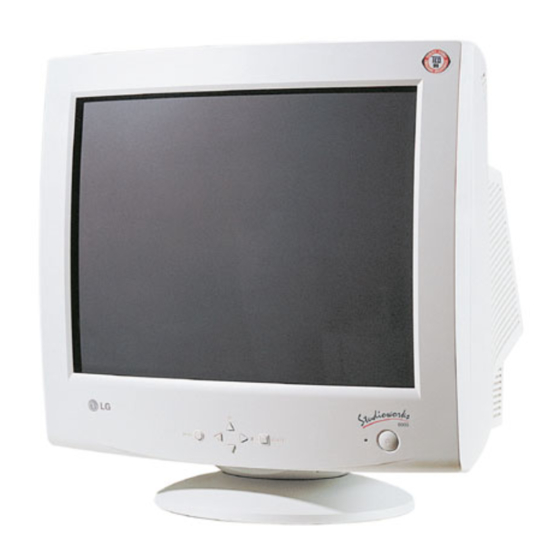
COLOR MONITOR
SERVICE MANUAL
CHASSIS NO. : CA-130
MODEL: StudioWorks 900B
(
) **Same model for SVC
CAUTION
BEFORE SERVICING THE UNIT,
READ THE SAFETY PRECAUTIONS IN THIS MANUAL.
MENU
SELECT
Website:http://biz.LGservice.com
E-mail:http://www.LGEservice.com/techsup.html
(900BJ-AL**E)
*Same looking with new chassis.
Issue Date; 2003. 6.
Advertisement
Table of Contents

Related Manuals for LG StudioWorks 900B


Summary of Contents for LG StudioWorks 900B
-
Page 1: Color Monitor
Website:http://biz.LGservice.com E-mail:http://www.LGEservice.com/techsup.html COLOR MONITOR SERVICE MANUAL CHASSIS NO. : CA-130 MODEL: StudioWorks 900B (900BJ-AL**E) ) **Same model for SVC CAUTION BEFORE SERVICING THE UNIT, READ THE SAFETY PRECAUTIONS IN THIS MANUAL. MENU SELECT *Same looking with new chassis. Issue Date; 2003. 6. -
Page 2: Table Of Contents
CONTENTS SPECIFICATIONS ........... 2 DESCRIPTION OF BLOCK DIAGRAM....10 SAFETY PRECAUTIONS ........3 ADJUSTMENT ............12 TIMING CHART ............4 TROUBLESHOOTING GUIDE ......14 OPERATING INSTRUCTIONS ........ 5 EXPLODED VIEW..........21 CONTROL LOCATIONS ......... 6 REPLACEMENT PARTS LIST ......23 WIRING DIAGRAM .......... -
Page 3: Safety Precautions
SAFETY PRECAUTIONS SAFETY-RELATED COMPONENT WARNING! X-RADIATION There are special components used in this color monitor The only potential source of X-radiation is the picture tube. which are important for safety. These parts are marked However, when the high voltage circuitry is operating on the schematic diagram and the replacement properly there is no possibility of an X-radiation problem. -
Page 4: Timing Chart
TIMING CHART VIDEO SYNC FACTORY PRESET MODE MODE MARK MODE 1 MODE 2 MODE 3 MODE 4 VESA Sync Polarity – Frequency 43.269 53.674 68.677 91.146 µs Total Period 23.112 18.631 14.561 10.971 µs Video Active Time 17.778 14.222 10.836 8.127 µs Blanking Time... -
Page 5: Operating Instructions
OPERATING INSTRUCTIONS FRONT VIEW REAR VIEW ID Label MENU SELECT Power ON/OFF Button AC Power Socket See Front Control Panel Signal Connector Front Control Panel 5. MENU Button 3. SELECT Button 2. Power (DPMS) Indicator MENU SELECT 1. Power Button Buttons Button 1. -
Page 6: Control Locations
CONTROL LOCATIONS VR801 : High Voltage Adjustment (26kV) VR901: B Adjustment (190V Line) - 6 -... -
Page 7: Wiring Diagram
WIRING DIAGRAM Anode Cap DY-Pin DY Assembly Screw P801 P901 P201- P701 (Control PCB) P451 P402 P401 - 7 -... -
Page 8: Disassembly
DISASSEMBLY 1. TILT/SWIVEL & BACK COVER REMOVAL 1) Set the monitor face downward. 2) Pull the latch (a), carefully remove the Tilt/Swivel by pulling it upward. 3) Pressing the latch (b), Back cover by pushing it upward. 4) Release the latch (c). 5) Slide the Back Cover away from the Front Cabinet of the monitor. -
Page 9: Block Diagram
BLOCK DIAGRAM - 9 -... -
Page 10: Description Of Block Diagram
DESCRIPTION OF BLOCK DIAGRAM 1. Line Filter & Associated Circuit. 5. X-ray Protection. This is used for suppressing noise of power input line This circuit detects the rectified DC voltage comes flowing into the monitor and/or some noise generated from the FBT pin 4. If the high voltage of the FBT in this monitor flowing out through the power input reaches up to about 30kV (abnormal state), H.V control (IC802) detects. - Page 11 11. D/D Drive & Convert Circuit. 19. Image Rotation (Tilt) Circuit. This circuit is used for supplying B + voltage to This circuit corrects the tilt of the screen by supplying horizontal deflection output transistor (Q801). This the image rotation signal to the tilt coil which is circuit makes to add side-pincushion correcting signal attached to the CDT near the deflection.
-
Page 12: Adjustment
ADJUSTMENT GENERAL INFORMATION 3) EEPROM ALL CLEAR Y(Yes) command. <Caution> Do not run this procedure unless the All adjustment are thoroughly checked and corrected EEPROM is changed. All data in EEPROM (mode when the monitor leaves the factory, but sometimes data and color data) will be erased. - Page 13 ± 0.05FL of 5. Input EDID Data. 11) Adjust SUB-Brightness command to 0.4 1) Display color 15,0 cross hatch pattern at Mode 4. the raster luminance. 12) Display color 15,0 Full White pattern(70x70mm) at 2) EEPROM Write EDID command and confirm mode 4.
-
Page 14: Troubleshooting Guide
TROUBLESHOOTING GUIDE 1. NO POWER NO POWER (POWER INDICATOR OFF) CHECK TROUBLE IN FUSE OK? FUSE (F901) (F901) CHECK TROUBLE IN D901 BRIDGE DIODE BRIDGE DIODE? (D901) CHECK C905(+) VOLTAGE 145VDC at 110V input TROUBLE IN 310VDC at 220V input IC901 TROUBLE IN CHECK... - Page 15 2. NO CHARACTER NO CHARACTER TROUBLE IN CHECK P301, SIGNAL CABLE, IC302 PIN 5, 6, 7 ? PC SIGNAL CHECK TROUBLE IN IC302 PIN 19, 20, 21 IC302, P302 PIN 10 (5V) ? CHECK IC303 PIN 1, 3, 5 TROUBLE IN PIN10 (12V), IC303 PIN 6 (80V) ?
- Page 16 3. NO RASTER NO VIDEO (POWER INDICATOR GREEN or AMBER) CHECK AMBER POWER INDICATOR TROUBLE IN GREEN or AMBER ? P302 SIGNAL CABLE GREEN CHECK ROTATE SCREEN SCREEN CONTROL CONTROL KNOB TO KNOB OF FBT CLOCKWISE or COUNTER CLOCKWIES CHECK VOLTAGE AT D924/D926 CATHODE (190V) TROUBLE IN PRIMARY...
-
Page 17: No Vertical Deflection
4. NO VERTICAL DEFLECTION NO V-DEFLECTION (ONE HORIZONTAL LINE) CHECK TROUBLE IN IC601 Pin 3 T901 15V LINE (15V) ? CHECK TROUBLE IN IC601 PIN 7 T701 -47V LINE (47V)? CHECK TROUBLE IN IC801 PIN 12 IC801 (SAWTOOTH WAVE)? TROUBLE IN IC601, V-CIRCUIT - 17 -... - Page 18 5. TROUBLE IN DPM STAND-BY/SUSPEND/ DPMS OFF MODE FAILURE CHECK CHECK PC, IC401 (MICOM) INPUT H/V SYNC SIGNAL (PC IS NOT GOING INTO PIN 40, 41 (H/V INPUT) DPM MODE) SIGNAL? NO H/V SYNC SIGNAL CHECK TROUBLE IN IC401 PIN 9, 8 X401, IC401 WAVEFORM? CHECK...
- Page 19 6. NO DEGAUSSING NO DEGAUSSING CHECK TROUBLE IN IC401 PIN 6 IC401 (MICOM) (5V)? CHECK TROUBLE IN Q920 COLLECTOR D925 VOLTAGE (0.5V)? CHECK TROUBLE IN P901? P901 CHECK TROUBLE IN RL901? RL901 TROUBLE IN TH901, DEGAUSSING COIL - 19 -...
- Page 20 7. TROUBLE IN OSD NO OSD CHECK TROUBLE IN IC302 PIN 18 P302 (5V) ? CHECK IC302 PIN 24 TROUBLE IN (H-PULSE COMES IN ?) P302 CHECK IC302 PIN 1 TROUBLE IN (V-PULSE COMES IN?) P302 CHECK IC302 PIN 11, 12 TROUBLE IN (IS THERE ANY SIGNAL IC401...
- Page 21 - 21 -...
-
Page 22: Exploded View
CABINET ASSEMBLY, 900BJ BRAND TKC057A LIFE GOOD (DI-LOCAL) - For Australia 3091TKC065J CABINET ASSEMBLY, 900BJ BRAND TKC057A LOGO RED (DI-LOCAL) - For Panama 2423GG2E92E CDT(CIRC), M46QCG913X 13NPUD LG-PHILIPS DISPLAYS 95KHZ 29.1 MM - For Northern Hemisphere, Eguatorial 6318L19003A CDT(CIRC), M46QCG913X 13SPUD LG-PHILIPS 95KHZ 29.1MM FST - For Southern Hemisphere 6318L19003C CDT(CIRC), M46QCG913X 14KPUD LG-PHILIPS 95KHZ 29.1MM FST TCO - For India... -
Page 23: Replacement Parts List
REPLACEMENT PARTS LIST CAUTION: BEFORE REPLACING ANY OF THESE COMPONENTS, READ CAREFULLY THE SAFETY PRECAUTIONS IN THIS MANUAL. * NOTE SAFETY Mark AL ALTERNATIVE PARTS DATE: 2003. 7. 4. DATE: 2003. 7. 4. *S *AL LOC. NO. PART NO. DESCRIPTION / SPECIFICATION *S *AL LOC. - Page 24 DATE: 2003. 7. 4. DATE: 2003. 7. 4. *S *AL LOC. NO. PART NO. DESCRIPTION / SPECIFICATION *S *AL LOC. NO. PART NO. DESCRIPTION / SPECIFICATION DIODEs C834 0CN1040K949 0.1M 50V Z F TA52 D201 0DL305029BA LTL-305DJ-0C2 TP LITEON GREE C841 0CE476CR630 47UF SHL,SD 250V M FM5 BULK...
- Page 25 Q726 0TR555109AB 2N5551 TP SAMSUNG TO92 AMP COILs & COREs Q771 0TR920009AB KSP92 TP SAMSUNG TO92 HIGH V Q801 0TR558900BA 2SC5589(LG,W/M) BK TOSHIBA T FB201 125-155J BFS2550A0FG SAMWHA 2.5*5.0MM Q802 0TR471009AA KSD471AC-Y TP SAMSUNG TO92 FB301 125-022J FERRITE KQ-1 JS 3.5*5.0MM AX...
- Page 26 DATE: 2003. 7. 4. DATE: 2003. 7. 4. *S *AL LOC. NO. PART NO. DESCRIPTION / SPECIFICATION *S *AL LOC. NO. PART NO. DESCRIPTION / SPECIFICATION Q806 0TR471009AA KSD471AC-Y TP SAMSUNG TO92 R342 0RD0332A609 33 OHM 1/2 W (7.0) 5% TA52 Q807 0TR564009AB KSB564AC-YTA TP SANSUNG TO92...
- Page 27 DATE: 2003. 7. 4. DATE: 2003. 7. 4. *S *AL LOC. NO. PART NO. DESCRIPTION / SPECIFICATION *S *AL LOC. NO. PART NO. DESCRIPTION / SPECIFICATION R705 0RB0150K609 0.15 OHM 2 W 5% TA52 R822 0RN3601F409 3.6K 1/6W 1 TA52 R706 0RD1003Q609 100K 1/4W(3 5% TA52...
- Page 28 DATE: 2003. 7. 4. *S *AL LOC. NO. PART NO. DESCRIPTION / SPECIFICATION R924 0RD0152Q609 15 1/4W(3 5% TA52 R925 0RD1501Q609 1.50K 1/4W(3 5% TA52 R926 0RD4701Q609 4.70K 1/4W(3 5% TA52 R927 0RD1001Q609 1K 1/4W(3 5% TA52 R929 0RN0220H609 0.22 1/2W 5% TA52 R930 0RN0220H609 0.22 1/2W 5% TA52...
-
Page 29: Pin Configuration
PIN CONFIGURATION M24C08 Serial I C BUS EEPROM SYMBOL DESCRIPTION PSDIP8 (BN) 0.25mm Frame Chip Enable Input E0-E2 Serial Data Address Input/Output Serial Clock Write Control SO8 (MN) 150mil Width Supply Voltage Logic Dirgram TSSOP8 (DW) Ground 169mil Width M62501P /FP Teerminal Number and The facillty PIN CONFIGURATION(TOP VIEW) PIN NO. - Page 30 TDA4867J PHILIPS 32P, SDIP SYMBOL DESCRIPTION non-inverted input inverted input supply voltage OUTB output B OUTB ground TDA4867J OUTA output A OUTA flyback supply voltage V FB GUARD guard output GUARD FEEDB feedback inprt FEEDB Pin Configuration GUARO output/ power save mode GUARD FLYBACK CIRCUIT...
- Page 31 TDA4841PS PHLIPS 32P HFLB FOCUS XRAY HSMOD HPLL2 BSENS HCAP HREF BDRV HBUF PGND HPLL1 HDRV SGND TDA4841PS XSEL VCAP VREF EWDRV VAGC VOUT2 VSMOD VOUT1 ASCOR VSYNC HSYBC CLBL HUNLOCK Pin Configuration EHT compensaton Block Diagram via vertical size EHT compensation via horizontal size 1.2V...
-
Page 32: Schematic Diagram
SCHEMATIC DIAGRAM NOTICE Since this is a basic schematic diagram. The value of components and some partial connection are sucject to be changed for improvement without notice. - 32 - - 33 -... -
Page 33: Printed Circuit Board
PRINTED CIRCUIT BOARD 1. CONTROL BOARD (Component Side) 2. CONTROL BOARD (Solder Side) 3. MAIN BOARD (Component Side) 4. MAIN BOARD (Solder Side) - 34 - - 35 -... - Page 34 Jun. 2003 P/NO : 3828TSL076M Printed in Korea...