Table of Contents
Advertisement
FILE NO. 810-200801GR
SERVICE MANUAL
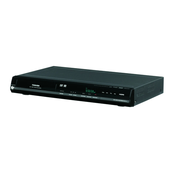
DVD Video Recorder
D-R410KU
D
V
D
V
D I
E
O
R
E
C
O
R
D
E
R
D
R -
4
0 1
The above model is classified as a green product (*1), as indicated by the underlined serial
number. This Service Manual describes replacement parts for the green product. When
repairing this green product, use the part(s) described in this manual and lead-free solder (*2).
For (*1) and (*2), see the next page.
TOSHIBA CORPORATION 2008
Published in Japan, Jan. 2008 GREEN
Advertisement
Table of Contents

Related Manuals for Toshiba D-R410KU


Summary of Contents for Toshiba D-R410KU
-
Page 1: Dvd Video Recorder
This Service Manual describes replacement parts for the green product. When repairing this green product, use the part(s) described in this manual and lead-free solder (*2). For (*1) and (*2), see the next page. TOSHIBA CORPORATION 2008 Published in Japan, Jan. 2008 GREEN... - Page 2 Hazardous Substances. From July 1, 2006, the RoHS Directive will prohibit any marketing of new products containing the restricted substances. Increasing attention is given to issues related to the global environmental. Toshiba Corporation recognizes environmental protection as a key management tasks, and is doing its utmost to enhance and improve the quality and scope of its environmental activities.
-
Page 3: Table Of Contents
It also is important to understand that these CAUTIONS and NOTICES ARE NOT EXHAUSTIVE. TOSHIBA could not possibly know, evaluate and advice the service trade of all conceivable ways in which service might be done or of the possible hazardous consequences of each way. -
Page 4: Specifications
SPECIFICATIONS General Input/Output System Video input [Input 1 (rear), 2 (front)] Input level : 1 Vp-p (75 Ω ) DVD-RW/-R ,DVD+RW/+R, DVD-Video, CD-DA, CD-RW/-R Jacks : RCA jack Power requirements Video output [Output 1 (rear)] Output level : 1 Vp-p (75 Ω ) AC120 V, 60 Hz Jack : RCA jack Power consumption... -
Page 5: Laser Beam Safety Precautions
LASER BEAM SAFETY PRECAUTIONS This DVD player uses a pickup that emits a laser beam. Do not look directly at the laser beam coming from the pickup or allow it to strike against your skin. The laser beam is emitted from the location shown in the figure. When checking the laser diode, be sure to keep your eyes at least 30 cm away from the pickup lens when the diode is turned on. -
Page 6: Important Safety Precautions
IMPORTANT SAFETY PRECAUTIONS Product Safety Notice K. When connecting or disconnecting the internal connectors, first, disconnect the AC plug from the Some electrical and mechanical parts have special AC outlet. safety-related characteristics which are often not evident from visual inspection, nor can the protection they give necessarily be obtained by replacing them with components rated for higher voltage, wattage, etc. - Page 7 Safety Check after Servicing Examine the area surrounding the repaired location for damage or deterioration. Observe that screws, parts, and wires have been returned to their original positions. Afterwards, do the following tests and confirm the specified values to verify compliance with safety standards. 1.
-
Page 8: Standard Notes For Servicing
STANDARD NOTES FOR SERVICING NOTE: BOARD MEANS PRINTED CIRCUIT BOARD. Circuit Board Indications Pb (Lead) Free Solder 1. The output pin of the 3 pin Regulator ICs is When soldering, be sure to use the Pb free solder. indicated as shown. How to Remove / Install Flat Pack-IC Top View Bottom View... - Page 9 3. The flat pack-IC on the BOARD is affixed with With Soldering Iron: glue, so be careful not to break or damage the foil 1. Using desoldering braid, remove the solder from of each pin or the solder lands under the IC when all pins of the flat pack-IC.
- Page 10 With Iron Wire: 2. Installation 1. Using desoldering braid, remove the solder from 1. Using desoldering braid, remove the solder from all pins of the flat pack-IC. When you use solder the foil of each pin of the flat pack-IC on the flux which is applied to all pins of the flat pack-IC, BOARD so you can install a replacement flat pack- you can remove it easily.
- Page 11 Instructions for Handling Semi- conductors Electrostatic breakdown of the semi-conductors may occur due to a potential difference caused by electrostatic charge during unpacking or repair work. 1. Ground for Human Body Be sure to wear a grounding band (1 MΩ) that is properly grounded to remove any static electricity that may be charged on the body.
-
Page 12: Cabinet Disassembly Instructions
CABINET DISASSEMBLY INSTRUCTIONS NOTE: BOARD MEANS PRINTED CIRCUIT BOARD. 1. Disassembly Flowchart Removal This flowchart indicates the disassembly steps to gain Remove/*Unhook/ Loc. Part Fig. Unlock/Release/ Note access to item(s) to be serviced. When reassembling, Unplug/Desolder follow the steps in reverse order. Bend, route, and dress the cables as they were originally. - Page 13 (S-7) (S-7) [6] BOARD POWER SUPPLY CN2204 [4] BOARD POWER SWITCH CN3002 (L-1) (S-3) (S-2) (L-1) (S-2) Fig. D4 [3] BOARD FRONT (L-1) (L-2) (S-10) (S-10) [2] PANEL FRONT Fig. D2 (S-5) (S-4) M-BOARD PLATE EARTH DVD MECHANISM [8] BOARD &...
- Page 14 3. How to Eject Manually Note: When rotating the gear, be careful not to damage the gear. 1. Remove the COVER TOP. 2. Rotate the gear in the direction of the arrow manually as shown below until the tray descends. 3.
-
Page 15: How To Initialize The Dvd Recorder
HOW TO INITIALIZE THE DVD RECORDER To put the program back at the factory-default, initialize the DVD recorder as the following procedure. 1. Turn the DVD recorder on. 2. Confirm that no disc is loaded or that the disc tray is open. -
Page 16: Firmware Renewal Mode
FIRMWARE RENEWAL MODE 1. Turn the power on and remove the disc on the tray. 4. Select the firmware version pressing arrow buttons, then press [ENTER]. 2. To put the DVD recorder into version up mode, Fig. d appears on the screen and Fig. e appears press [INSTANT SKIP], [6], [5], and [4] buttons on on the VFD. -
Page 17: Troubleshooting
TROUBLESHOOTING NOTE: BOARD MEANS PRINTED CIRCUIT BOARD. FLOW CHART NO.1 The power cannot be turned on. See FLOW CHART No.2 <The fuse blows out.> Is the fuse normal? Is normal state restored when once unplugged Check for lead or short-circuiting of primary power cord is plugged again after several seconds. - Page 18 FLOW CHART NO.6 EV+10.5V is not outputted. Check D1063, D1064, C1063, C1064, L1052 and their periphery, and replace P1(AV ASSEMBLY) if defective. FLOW CHART NO.7 P-ON+5V(AUDIO+5V) is not outputted. Check D1058, D1059, C1060, C1061, L1051 and their periphery, and replace P1(AV ASSEMBLY) Is 5V voltage supplied to the emitter of Q1053? if defective.
- Page 19 FLOW CHART NO.11 P-ON+1.8V is not outputted. Is 2.8V voltage supplied to Pin(1) of IC1504? Check D1056, C1058 and their periphery, and replace P1(AV ASSEMBLY) if defective. Replace P1(AV ASSEMBLY). FLOW CHART NO.12 P-ON+3.3V is not outputted. Is 5V voltage supplied to Pin(1) of IC1503? Check D1058, D1059, C1060 and their periphery, and replace P1(AV ASSEMBLY) if defective.
- Page 20 FLOW CHART NO.15 No operation is possible from the remote control unit. (Operation is possible from the unit.) Is 5V voltage supplied to the Pin(2) terminal of Check EV+5V line and replace P1(AV ASSEMBLY) or P3(BOARD FRONT) if defective. the RE3001 (remote control receiver)? Is the "L"...
- Page 21 FLOW CHART NO.18 VIDEO E-E does not appear normally. Are the video signals inputted to each pin of Check the line between video input terminal and IC1301? each pin of IC1301. → JK2106 IC1301 8PIN VIDEO-IN 1 (REAR) IC1301 8PIN VIDEO-IN 1 (REAR) →...
- Page 22 Are the video signals outputted to the specific output terminal? Are the luminance signals outputted to the Check the periphery of JK2202 from Pin (13) of S-VIDEO OUT terminal (JK2202)? IC1401 and replace P1(AV ASSEMBLY) if defective. Are the chroma signals outputted to the Check the periphery of JK2202 from Pin (15) of S-VIDEO OUT terminal (JK2202)? IC1401 and replace P1(AV ASSEMBLY) if defective.
- Page 23 Are the video signals outputted to the specific output terminal? Are the luminance signals outputted to the Check the periphery of JK2202 from Pin (13) of S-VIDEO OUT terminal (JK2202)? IC1401 and replace P1(AV ASSEMBLY) if defective. Are the chroma signals outputted to the Check the periphery of JK2202 from Pin (15) of S-VIDEO OUT terminal (JK2202)? IC1401 and replace P1(AV ASSEMBLY) if defective.
- Page 24 Are the analog audio signals outputted to each pin of IC1201? IC1201 7PIN AUDIO (L)-OUT Replace P1(AV ASSEMBLY). IC1201 1PIN AUDIO (R)-OUT Are the analog audio signals outputted to each pin Is the "L" pulse inputted to Pin (9, 10, 11) of IC1022? of IC1022? IC1022 14PIN AUDIO (L)-OUT Check the line between Pin (9,...
-
Page 25: Function Indicator Symbols
FUNCTION INDICATOR SYMBOLS Note: If an error occurs, a message with the error number appears on the screen. Recording Error Error message You cannot record on this disc as Power Calibration Area is full. Error No. Error Message Solution Error Description Priority An error occurs during data reading. - Page 26 Error Message Solution Error Description Priority Release the disc protect This disc is protected and not setting in the Disc Setting Disc Protected Disc. recordable. menu. Disc is full. Insert the recordable disc with No available recording space. (No area for new recording) enough recording space.
-
Page 27: Block Diagrams
BLOCK DIAGRAMS System Control Block Diagram NOTE: BOARD MEANS PRINTED CIRCUIT BOARD. IC1501 (SUB MICRO CONTROLLER) IC1502 Q1501 REG-CONT2 26 REG-CONT2 RESET RESET EV+3.3V POW-SW TO POWER SUPPLY POW-SW REG-CONT BLOCK DIAGRAM REG-CONT PWSW PWSW P-DOWN Q1502 EV+5V X1501 C1501 (BACKUP CAPACITOR) X OUT 8MHz... - Page 28 Digital Signal Process Block Diagram NOTE: BOARD MEANS PRINTED CIRCUIT BOARD. REC VIDEO SIGNAL PB VIDEO SIGNAL REC AUDIO SIGNAL PB AUDIO SIGNAL DVD MECHANISM IC101 (MAIN MICRO CONTROLLER/MPEG2 AV CODEC) IC201 VIDEO-Y(I/P) VIDEO-C VIDEO-Pb/Cb ERROR AMP VIDEO VIDEO-Pr/Cr ENCODER VIDEO CN201 A5,B5-B7...
-
Page 29: Video Block Diagram
Video Block Diagram NOTE: BOARD MEANS PRINTED CIRCUIT BOARD. REC VIDEO SIGNAL PB VIDEO SIGNAL REC AUDIO SIGNAL PB AUDIO SIGNAL POFF-SELECT TO SYSTEM CONTROL DVD MAIN BOARD BOARD AV BLOCK DIAGRAM IC1022 (INPUT SELECT) Q1601 BUFFER SW CTL W F 3 JK2202 S-VIDEO OUT C1231... -
Page 30: Audio Block Diagram
Audio Block Diagram NOTE: BOARD MEANS PRINTED CIRCUIT BOARD. REC AUDIO SIGNAL PB AUDIO SIGNAL W F 7 JK2206 CN101 CN1051 Q1241 SPDIF SPDIF BUFFER DIGITAL REAR AUDIO OUT (COAXIAL) IC1201 (OP AMP) W F 6 CN701 CN1101 AUDIO(L)-OUT AUDIO(L)-OUT AUDIO(R)-OUT AUDIO(R)-OUT DVD-AUDIO-MUTE... -
Page 31: Power Supply Block Diagram
Power Supply Block Diagram NOTE: BOARD MEANS PRINTED CIRCUIT BOARD. CAUTION ! CAUTION ! NOTE: Fixed voltage (or Auto voltage selectable) power supply circuit is used in this unit. For continued protection against fire hazard, The voltage for parts in hot circuit is measured using If Main Fuse (F1001) is blown , check to see that all components in the power supply replace only with the same type fuse. -
Page 32: Schematic Diagrams / Board's And Test Points
SCHEMATIC DIAGRAMS / BOARD’S AND TEST POINTS NOTE: BOARD MEANS PRINTED CIRCUIT BOARD. Standard Notes WARNING Many electrical and mechanical parts in this chassis have special characteristics. These characteristics often pass unnoticed and the protection afforded by them cannot necessarily be obtained by using replacement components rated for higher voltage, wattage, etc. - Page 33 LIST OF CAUTION, NOTES, AND SYMBOLS USED IN THE SCHEMATIC DIAGRAMS ON THE FOLLOWING PAGES: 1. CAUTION: FOR CONTINUED PROTECTION AGAINST FIRE HAZARD, REPLACE ONLY WITH THE SAME TYPE FUSE. ATTENTION: POUR UNE PROTECTION CONTINUE LES RISQES D'INCELE N'UTILISER QUE DES FUSIBLE DE MÊME TYPE. RISK OF FIRE-REPLACE FUSE AS MARKED.
- Page 34 AV 1/4 Schematic Diagram * NOTE NOTE: BOARD MEANS PRINTED CIRCUIT BOARD. These components (IC1502A, C1509A, IC1502B, C1509B) can be used in any models. However, you cannot mix components under Group A with the ones under Group B. You can choose either Group. The difference between Group A and Group B is shown below.
- Page 35 AV 2/4 Schematic Diagram NOTE: BOARD MEANS PRINTED CIRCUIT BOARD. 1-11-4 E7K7ASCAV2...
- Page 36 AV 3/4 Schematic Diagram NOTE: BOARD MEANS PRINTED CIRCUIT BOARD. 1-11-5 E7K7ASCAV3...
- Page 37 AV 4/4 Schematic Diagram NOTE: BOARD MEANS PRINTED CIRCUIT BOARD. E7K7ASCAV4 1-11-6...
- Page 38 POWER SUPPLY Schematic Diagram NOTE: BOARD MEANS PRINTED CIRCUIT BOARD. CAUTION ! CAUTION ! NOTE: For continued protection against fire hazard, Fixed voltage (or Auto voltage selectable) power supply circuit is used in this unit. The voltage for parts in hot circuit is measured using If Main Fuse (F1001) is blown , check to see that all components in the power supply replace only with the same type fuse.
- Page 39 FRONT & POWER SWITCH Schematic Diagram FL3001 MATRIX CHART NOTE: BOARD MEANS PRINTED CIRCUIT BOARD. BS CS DR DTV BS CS 1-11-8 E7K7ASCF...
- Page 40 DVD Main 1/7 Schematic Diagram NOTE: BOARD MEANS PRINTED CIRCUIT BOARD. 1 NOTE: The order of pins shown in this diagram is different from that of actual IC101. IC101 is divided into six and shown as IC101 (1/6) ~ IC101 (6/6) in this DVD Main Schematic Diagram Section. 1-11-9 E7K7ASCD1...
- Page 41 DVD Main 2/7 Schematic Diagram NOTE: BOARD MEANS PRINTED CIRCUIT BOARD. 1 NOTE: The order of pins shown in this diagram is different from that of actual IC101. IC101 is divided into six and shown as IC101 (1/6) ~ IC101 (6/6) in this DVD Main Schematic Diagram Section. 1-11-10 E7K7ASCD2...
- Page 42 DVD Main 3/7 Schematic Diagram NOTE: BOARD MEANS PRINTED CIRCUIT BOARD. 1 NOTE: The order of pins shown in this diagram is different from that of actual IC101. IC101 is divided into six and shown as IC101 (1/6) ~ IC101 (6/6) in this DVD Main Schematic Diagram Section. 1-11-11 E7K7ASCD3...
- Page 43 DVD Main 4/7 Schematic Diagram NOTE: BOARD MEANS PRINTED CIRCUIT BOARD. 1 NOTE: The order of pins shown in this diagram is different from that of actual IC101. IC101 is divided into six and shown as IC101 (1/6) ~ IC101 (6/6) in this DVD Main Schematic Diagram Section. 1-11-12 E7K7ASCD4...
- Page 44 DVD Main 5/7 Schematic Diagram NOTE: BOARD MEANS PRINTED CIRCUIT BOARD. 1 NOTE: The order of pins shown in this diagram is different from that of actual IC101. IC101 is divided into six and shown as IC101 (1/6) ~ IC101 (6/6) in this DVD Main Schematic Diagram Section. 1-11-13 E7K7ASCD5...
- Page 45 DVD Main 6/7 Schematic Diagram NOTE: BOARD MEANS PRINTED CIRCUIT BOARD. 1-11-14 E7K7ASCD6...
- Page 46 DVD Main 7/7 Schematic Diagram NOTE: BOARD MEANS PRINTED CIRCUIT BOARD. 1 NOTE: The order of pins shown in this diagram is different from that of actual IC101. IC101 is divided into six and shown as IC101 (1/6) ~ IC101 (6/6) in this DVD Main Schematic Diagram Section. 1-11-15 E7K7ASCD7...
- Page 47 BOARD AV Top View NOTE: BOARD MEANS PRINTED CIRCUIT BOARD. 1-11-16 BE7K2AF01011A...
- Page 48 BOARD AV Bottom View NOTE: BOARD MEANS PRINTED CIRCUIT BOARD. C1231 PLUS LEAD PIN 1 OF CN1101 PIN 3 OF CN1101 PIN 5 OF CN1101 PIN 7 OF CN1101 PIN 15 OF CN1101 PIN 3 OF CN1051 1-11-17 BE7K2AF01011A...
- Page 49 BOARD POWER SUPPLY Top View NOTE: BOARD MEANS PRINTED CIRCUIT BOARD. NOTE: CAUTION ! CAUTION ! The voltage for parts in hot circuit is measured using Fixed voltage (or Auto voltage selectable) power supply circuit is used in this unit. For continued protection against fire hazard, hot GND as a common terminal.
- Page 50 BOARD POWER SUPPLY Bottom View NOTE: BOARD MEANS PRINTED CIRCUIT BOARD. NOTE: CAUTION ! CAUTION ! The voltage for parts in hot circuit is measured using Fixed voltage (or Auto voltage selectable) power supply circuit is used in this unit. For continued protection against fire hazard, hot GND as a common terminal.
- Page 51 BOARD FRONT Top View BOARD POWER SWITCH Top View NOTE: BOARD MEANS PRINTED CIRCUIT BOARD. BOARD FRONT Bottom View BOARD POWER SWITCH Bottom View BE7H70F01032 BE7K2AF01011D 1-11-20...
-
Page 52: Waveforms
WAVEFORMS Pin 5 of CN1101 Pin 3 of CN1101 VIDEO-Y 0.2V 20μsec VIDEO-Cr 0.2V 20μsec Pin 7 of CN1101 Pin 15 of CN1101 VIDEO-C 0.2V 20μsec AUDIO(L)-OUT 0.5ms C1231 PLUS LEAD Pin 3 of CN1051 VIDEO-CVBS 0.5V 20μsec SPDIF 0.1μsec Pin 1 of CN1101 NOTE: Input: COLOR BAR SIGNAL... -
Page 53: Wiring Diagram
WIRING DIAGRAM NOTE: BOARD MEANS PRINTED CIRCUIT BOARD. REAR FRONT CN1060 CN1070 DIGITAL VIDEO VIDEO EV+10.5V S-VIDEO S-VIDEO VIDEO AUDIO AUDIO VIDEO VIDEO AUDIO AUDIO S-VIDEO VIDEO AUDIO(L) AUDIO(R) AUDIO OUT -Pb/Cb -Pr/Cr EV+10.5V -IN1 (L)-IN1 (R)-IN1 -Y OUT -OUT (L)-OUT (R)-OUT (COAXIAL) -
Page 54: System Control Timing Charts
SYSTEM CONTROL TIMING CHARTS [ Tray Open ] Push Close Power on button is pressed. Tray insertion INNER-SW open? Tray insertion INNER-SW open? Tray ejection To disc distinction [ Tray Open ] button is pressed. INNER-SW open? SLED moves Tray ejection 1-14-1 R5NTI... - Page 55 Parameter V*: Voltage T*: Event timer V0: 2.40 V T1: 0.125 s V1: 4.664 V T2: 3.000 s V2: 2.020 V T3: 0.050 s V3: 2.386 V T4: 0.060 s V4: 4.302 V T5: 0.600 s T6: 1.400 s T7: 1.600 s T8: 0.050 s Tray open Tray ejection direction...
- Page 56 Push close Threshold level 0.08 V 0.02 s Push Close detection 1-14-3 R5NTI...
-
Page 57: Ic Pin Function Descriptions
IC PIN FUNCTION DESCRIPTIONS IC1501 (SUB MICRO CONTROLLER) Signal Function Name Signal Function Not Used Name Not Used IN KEY-1 Key Data Input 1 POFF- IN KEY-2 Key Data Input 2 37 OUT Power Off Select Signal SELECT IN POW-SW Abnormal Voltage Detection Not Used IN AFT... - Page 58 IC3001 (VFD DRIVER) Signal Function Name IN CLK FL Serial Clock IN STB Serial Interface Strobe Not Used Not Used Ground IN VDD +3.3V Power Supply Segment Output IN VEE Pull Down Level 16 OUT P7 Segment Output Grid Output IN VDD +3.3V Power Supply IN OSC...
-
Page 59: Lead Identifications
LEAD IDENTIFICATIONS KIA4558F-EL/P KTC3203-Y-AT/P KTA1267-GR-AT/P 2SK3757(Q) KTA1271-Y-AT/P KRC103M-AT/P KTC3199-(BL, GR)-AT/P KTA1266-GR-AT/P G D S E C B E C B MM1697AJBE PQ070XFC1SZF KTB1151-Y-U/P MM1637XVBE 1 2 3 4 B C E MN101C77AFT 4052L-S16-R BU4219G-TR PS2561A-1(W) 4053L-S16-R R3112N191A-TR-FA R3112N191A-TR-FB PST3619NR 1: Anode 2: Cathode 3: Emitter 4: Collector... - Page 61 (P1) AV ASSEMBLY AC1001 CN1701 F1001 CN1070 CN1101 BOARD POWER SUPPLY CN1051 ( P1 ) AV ASSEMBLY BOARD AV BOARD POWER SWITCH CN1064 1-17-2 E7K7ACEX...
- Page 62 (P2) DVD MECHANISM & DVD MAIN BOARD ASSEMBLY ( P2 ) DVD MECHANISM & DVD MAIN BOARD ASSEMBLY (P3) BOARD FRONT CN3001 ( P3 ) BOARD FRONT 1-17-3 E7K7ACEX...
- Page 63 Packing Upper Side Lower Side X22B X22A Some Ref. Numbers are not in sequence. Unit 1-17-4 E7K7APEX...
-
Page 64: Mechanical Parts List
MECHANICAL PARTS LIST PRODUCT SAFETY NOTE: Products marked with a ! have special characteristics important to safety. Before replacing any of these components, read carefully the product safety notice in this service manual. Don't degrade the safety of the product through improper servicing. -
Page 65: Electrical Parts List
ELECTRICAL PARTS LIST PRODUCT SAFETY NOTE: Products marked with a ! have special characteristics important to safety. Before replacing any of these components, read carefully the product safety notice in this service manual. Don't degrade the safety of the product through improper servicing.