Table of Contents
Advertisement
Quick Links
IMPORTANT INFORMATION ABOUT LEAD FREE, (PbF), SOLDERING
If lead free solder was used in the manufacture of this product the printed circuit boards will be marked PbF, Standard laded, (Pb),
solder can be used as usual on boards without the PbF mark.
When this mark does appear please read and follow the special instructions described in this manual on the use of PbF and how
it might be permissible to use Pb solder during service and repair work.
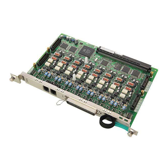
16-Port Analogue Trunk Card
KX-TDA6181X
(for Asia, Oceania, Middle Near East, Latin America,
Russia and Africa)
© 2005 Panasonic Communications Co., Ltd. All
rights
reserved.
distribution is a violation of law.
ORDER NO. KMS0510155CE
Unauthorized
copying
and
Advertisement
Table of Contents

Related Manuals for Panasonic KX-TDA6181X


Summary of Contents for Panasonic KX-TDA6181X
- Page 1 When this mark does appear please read and follow the special instructions described in this manual on the use of PbF and how it might be permissible to use Pb solder during service and repair work. © 2005 Panasonic Communications Co., Ltd. All rights reserved.
-
Page 2: Table Of Contents
KX-TDA6181X CONTENTS Page Page 1 ABOUT LEAD FREE SOLDER (PbF: Pb free) 10 HOW TO REPLACE A FLAT PACKAGE IC 1.1. SUGGESTED PBF SOLDER 10.1. PREPARATION 1.2. HOW TO RECOGNIZE THAT Pb FREE SOLDER IS 10.2. REMOVAL PROCEDURE USED 10.3. INSTALLATION PROCEDURE 2 FOR SERVICE TECHNICIANS 10.4. -
Page 3: About Lead Free Solder (Pbf: Pb Free)
KX-TDA6181X 1 ABOUT LEAD FREE SOLDER (PbF: Pb free) Note: In the information below, Pb, the symbol for lead in the periodic table of elements, will refer to standard solder or solder that contains lead. We will use PbF solder when discussing the lead free solder used in our manufacturing process which is made from Tin, (Sn), Silver, (Ag), and Copper, (Cu). -
Page 4: How To Recognize That Pb Free Solder Is Used
KX-TDA6181X 1.2. HOW TO RECOGNIZE THAT Pb FREE SOLDER IS USED... -
Page 5: For Service Technicians
KX-TDA6181X 2 FOR SERVICE TECHNICIANS ICs and LSIs are vulnerable to static electricity. When repairing, the following precautions will help prevent recurring malfunctions. 1. Cover the plastic part´s boxes with aluminum foil. 2. Ground the soldering irons. 3. Use a conductive mat on the worktable. -
Page 6: System Construction
KX-TDA6181X 5 SYSTEM CONSTRUCTION... -
Page 7: Installing/Removing The Optional Service Cards
KX-TDA6181X 5.1. INSTALLING/REMOVING THE OPTIONAL SERVICE CARDS Slot Condition Card Type Slot Type KX-TDA600 KX-TDA620 Free 1-10 EMPR BUS-M Free 1-11 BUS-S EMPR Card BUS-M Card BUS-S Card Trunk Cards Extension Cards OPB3 Card CTI-LINK Card EECHO Card Caution: To protect the back board from static electricity, do not touch parts on the back board in the main unit and on the optional service cards.To discharge static, touch ground or wear an earthing strap. - Page 8 KX-TDA6181X Pin Assignments Amphenol Connector No. Signal Name Function No. Signal Name Function Ring port 1 26 TA Tip port 1 Ring port 2 27 TB Tip port 2 Ring port 3 28 TC Tip port 3 Ring port 4...
- Page 9 KX-TDA6181X In case of install CID/PAY8 on ELCOT16 card Function CID/PAY8: 8-port Caller ID signal type FSK/FSK (with Visual Caller ID)/DTMF, and 8 ports of Pay Tone Service (12 kHz/16kHz).To be mounted on the ELCOT16 cards. CID8: 8-port Caller ID signal type FSK/FSK (with Visual Caller ID)/DTMF, To be mounted on the ELCOT16 cards.
- Page 10 KX-TDA6181X Fastening Amphenol Type Connector An amphenol 57JE type connector is used on some of the optional sevice cards. To connect an amphenol connector, use the spring latch or screw to fix the upper part and use Velcro tape to fix the lower...
- Page 11 KX-TDA6181X Using Analogue Trunk Card and Extension Card Power Failure Connection connects a specific SLT and a trunk in the event of power failure. The following analogue trunk and extension cards can be used for Power Failure Connections: • • • • Analogue trunk card: ELCOT16 (4 PFT ports) •...
- Page 12 KX-TDA6181X RJ11 Connector Pin Assignments for Analogue Trunk Card PFT Ports 1 and 2 No. Signal Name Function Ring port 2 Ring port 1 Tip port 1 Tip port 2 PFT Ports 3 and 4 No. Signal Name Function Ring port 4...
- Page 13 KX-TDA6181X Installing Optional Service Cards 1. Insert the card along the guide rails. 2. Holding the card as follows, push the release lever in the direction of the arrow so that the card is made to engage with the connector on the back board securely.
-
Page 14: Block Diagram
D[15:0] Port#7 Same as "Port#1" Ring nRESET Ring IC402 nCS0 Flash A[19:0] Ring D[15:0] Port#8 Same as "Port#1" Ring Ring nCS2 IC403 Power +15V PORT#5-#8 PORT#9-#12(NO PFT) Supply +3.3V A[16:0] PORT#13-#16(NO PFT) D[7:0] Diag-Tip, Diag-Ring KX-TDA6181X ELCOT16 CARD BLOCK DIAGRAM... -
Page 15: Circuit Operations
KX-TDA6181X 7 CIRCUIT OPERATIONS 7.1. CONTROL-SYSTEM CIRCUIT 7.1.1. CPU Peripherals • • • • CPU (System clock: 12.288 MHz)..IC401 Data bus: 16bit, Address bus: 23bit • • • • Flash ROM (512Kbyte)..IC402 Flash memory consists of two areas: boot space and administration space. - Page 16 KX-TDA6181X Orange: OUS (Because OUS needs to be controlled by EMPR, reset terminal and port control terminal are ORed to generate OUS) • • • • Instantaneous power interruption operation When instantaneous power interruption is 300msec or less, reset operation is not carried out because the voltage is retained by the capacitor in the power supply.
- Page 17 KX-TDA6181X 7.1.2. Time Slot Configuration PCM data of an arbitrary stream, 0 - 15 (1 stream equals 128 time slots), on H.100 bus can be switched to an arbitrary local highway (64 time slots) using a local TSW. An example of time slot configuration of a local highway in ELCOT16 is shown below.
- Page 18 KX-TDA6181X 7.1.3. IC3 (ASIC) • • • • EC bus interface 16bit/8MHz two-way address data multiplex self-bus. • • • • CT bus interface Supports eight 8.192MHz highways (128 time slots). • • • • Local bus Interface SH-1CPU by RENESAS Ltd. compatible bus with 8-bit data and 13bit address.
-
Page 19: Description Of Functions And Circuits
KX-TDA6181X 7.2. DESCRIPTION OF FUNCTIONS AND CIRCUITS 7.2.1. Dial Pulse Signal Transmission Transmits 10pps/20pps dial pulse by a open/close action between Tip and Ring with Photo MOS relay. The make width, break width and inter digital width for 10pps/20pps can be set respectively. - Page 20 KX-TDA6181X 7.2.4. Bell Signal Detection During on-hook, transmitting the bell signal to the AC loop in the CR series circuits (C2 and R2) detects the current by Photo Coupler (PC1,2), and it determines the presence of a bell signal. Software performs the operation for recognition and determination of a pattern of bell signals.
- Page 21 KX-TDA6181X 7.2.7. 2W-4W Conversion This converts 4W-voice signal inside PBX and 2W-voice signal on SLT or Trunk. It is configured by Op-Amp and BN (Balance Network) in CODEC. It affects the return loss of the voice and the frequency characteristic, and is determined by setting the best value of Infineon CODEC and a software register.
-
Page 22: Power Supply Circuit
KX-TDA6181X 7.2.10. Power Failure Port At the time of the power failure, for enabling a direct call to the extension phone, 4lines out of 16lines can be connected to the SLT port, which provides a switching relay for power failure on the extension card, by a cable. It connects CN3, CN4 with the connector for power failure on the extension card. - Page 23 KX-TDA6181X 7.3.1. Power Supply System It provides four power systems; +15V power input and +5V, +3.3V power output.
-
Page 24: Troubleshooting Guide
KX-TDA6181X 8 TROUBLESHOOTING GUIDE... - Page 25 KX-TDA6181X...
- Page 26 KX-TDA6181X...
- Page 27 KX-TDA6181X...
- Page 28 KX-TDA6181X...
- Page 29 KX-TDA6181X...
-
Page 30: Ic Data
KX-TDA6181X 9 IC DATA 9.1. IC3 (ASIC) Pin No. Pin Name Signal Name Description OT_OE15 DTMF data output control signal OT_OE14 DTMF data output control signal OT_OE13 DTMF data output control signal OT_OE12 DTMF data output control signal OT_OE11 DTMF data output control signal... - Page 31 KX-TDA6181X Pin No. Pin Name Signal Name Description DT_OE1 DTMF data output control signal DT_OE0 DTMF data output control signal Reserve Reserve Reserve Reserve Reserve Reserve Reserve Reserve...
-
Page 32: Ic6 (Codec)
KX-TDA6181X 9.2. IC6 (CODEC) Line wire Pin No. Pin Name Signal Name Description port SO1_1 SHNT0 Pulse Control/Bell Receive Control SO1_0 DIAG0 Self-Diagnosis Switching SB1_2 DIAL0 Line Acquisition SB1_1 BELLI0 Receiving Bell Signal SB1_0 REVDET0 H/L Line Reversal Detection SI1_1... -
Page 33: Ic7 (Codec)
KX-TDA6181X 9.3. IC7 (CODEC) Line wire Pin No. Pin Name Signal Name Description port SO1_1 SHNT4 Pulse Control/Bell Receive Control SO1_0 DIAG4 Self-Diagnosis Switching SB1_2 DIAL4 Line Acquisition SB1_1 BELLI4 Receiving Bell Signal SB1_0 REVDET4 H/L Line Reversal Detection SI1_1... -
Page 34: Ic9 (Codec)
KX-TDA6181X 9.4. IC9 (CODEC) Line wire Pin No. Pin Name Signal Name Description port SO1_1 SHNT8 Pulse Control/Bell Receive Control SO1_0 DIAG8 Self-Diagnosis Switching SB1_2 DIAL8 Line Acquisition SB1_1 BELLI8 Receiving Bell Signal SB1_0 REVDET8 H/L Line Reversal Detection SI1_1... -
Page 35: Ic10 (Codec)
KX-TDA6181X 9.5. IC10 (CODEC) Line wire Pin No. Pin Name Signal Name Description port CO13 SO1_1 SHNT12 Pulse Control/Bell Receive Control SO1_0 DIAG12 Self-Diagnosis Switching SB1_2 DIAL12 Line Acquisition SB1_1 BELLI12 Receiving Bell Signal SB1_0 REVDET12 H/L Line Reversal Detection... -
Page 36: Ic601 (Cpu) I/O Map
KX-TDA6181X 9.6. IC601 (CPU) I/O MAP Pin No. Pin name Signal name Description Remarks PA15 PA14 PA13 nIRQ1 EMPR interrupt Used as nIRQ1 PA12 HALT DC power down recovery detection Used as nIRQ0 PA11 nRTS Serial I/F for debug PA10... -
Page 37: How To Replace A Flat Package Ic
KX-TDA6181X 10 HOW TO REPLACE A FLAT PACKAGE IC Even if you do not have the special tools (for example, a spot heater) to remove the Flat IC, with some solder (large amount), a soldering iron and a cutter knife, you can easily remove the ICs that have more than 100 pins. -
Page 38: Terminal Guide Of Ics, Transistors And Diodes
KX-TDA6181X 11 TERMINAL GUIDE OF ICs, TRANSISTORS AND DIODES... -
Page 39: Cabinet And Electrical Parts Location
KX-TDA6181X 12 CABINET AND ELECTRICAL PARTS LOCATION... -
Page 40: Accessories And Packing Material
KX-TDA6181X 13 ACCESSORIES AND PACKING MATERIAL... -
Page 41: Replacement Parts List
KX-TDA6181X 14 REPLACEMENT PARTS LIST 1. RTL (Retention Time Limited) Ref. Part No. Part Name & Description Remarks The marking (RTL) indicates that the Retention Time is PSUS1021Y TORSION SPRING limited for this item. XUC25VW RETAINING RING After the discontinuation of this assembly in production, the 14.2. - Page 42 KX-TDA6181X Ref. Part No. Part Name & Description Remarks Ref. Part No. Part Name & Description Remarks B1BBDL000007 TRANSISTOR(SI) PQVDRLZ2R0B DIODE(SI) B1BBDL000007 TRANSISTOR(SI) PQVDRLZ2R0B DIODE(SI) B1BBDL000007 TRANSISTOR(SI) MA8075 DIODE(SI) B1BBDL000007 TRANSISTOR(SI) PQVDRLZ2R0B DIODE(SI) B1BBDL000007 TRANSISTOR(SI) PQVDRLZ2R0B DIODE(SI) B1GBCFGG0009 TRANSISTOR(SI) PQVDRLZ2R0B...
- Page 43 KX-TDA6181X Ref. Part No. Part Name & Description Remarks Ref. Part No. Part Name & Description Remarks RA1M D1H86814A024 RESISTOR ARRAY, 680 J0JHC0000060 IC FILTER RA1N D1H86814A024 RESISTOR ARRAY, 680 J0JHC0000060 IC FILTER RA1O D1H86814A024 RESISTOR ARRAY, 680 J0JHC0000060 IC FILTER...
- Page 44 KX-TDA6181X Ref. Part No. Part Name & Description Remarks Ref. Part No. Part Name & Description Remarks J0JAD0000036 IC FILTER PC5D PQVIP27011M3 PHOTO COUPER J0JAD0000036 IC FILTER PC5E PQVIP27011M3 PHOTO COUPER J0JAD0000036 IC FILTER PC5F PQVIP27011M3 PHOTO COUPER J0JAD0000036 IC FILTER...
- Page 45 KX-TDA6181X Ref. Part No. Part Name & Description Remarks Ref. Part No. Part Name & Description Remarks SA1G J0LE00000043 VARISTOR (SURGE ABSORBER) EEEFK1H100UR SA1H J0LE00000043 VARISTOR (SURGE ABSORBER) EEEFK1H100UR SA1I J0LE00000043 VARISTOR (SURGE ABSORBER) EEEFK1H100UR SA1J J0LE00000043 VARISTOR (SURGE ABSORBER)
- Page 46 KX-TDA6181X Ref. Part No. Part Name & Description Remarks Ref. Part No. Part Name & Description Remarks F1G1H220A565 F1G0J2240003 0.22 F1G1H220A565 F1G1A1040006 F1G1H220A565 F1G1A1040006 F1G1H220A565 F1G1A1040006 F1G1H220A565 F1G1A1040006 F1G1H220A565 PQCUV1H105JC F1G1H220A565 F1G0J2240003 0.22 F1G1H220A565 F1G1A1040006 F1G1H220A565 F1G1A1040006 F1G1H220A565 F1G1A1040006 F1G1H220A565...
- Page 47 KX-TDA6181X Ref. Part No. Part Name & Description Remarks Ref. Part No. Part Name & Description Remarks C408 F1G1H103A573 0.01 PQ4R18XJ000 C409 F1G1H103A573 0.01 PQ4R18XJ000 C410 F1G1H103A573 0.01 PQ4R18XJ000 C411 F1G1H103A573 0.01 PQ4R18XJ000 C412 F1G1H103A573 0.01 PQ4R18XJ000 C413 ECUV1A105ZFV PQ4R18XJ000...
- Page 48 KX-TDA6181X Ref. Part No. Part Name & Description Remarks Ref. Part No. Part Name & Description Remarks ERJ2GEYJ151 R11G ERJ2RHD104 100K ERJ8GEYJ390 R11H ERJ2RHD104 100K ERJ8GEYJ390 R11I ERJ2RHD104 100K ERJ8GEYJ390 R11J ERJ2RHD104 100K ERJ8GEYJ390 R11K ERJ2RHD104 100K ERJ8GEYJ390 R11L ERJ2RHD104...
- Page 49 KX-TDA6181X Ref. Part No. Part Name & Description Remarks Ref. Part No. Part Name & Description Remarks R15O ERJ2RHD563 R51D PQ4R10XJ122 1.2K R15P ERJ2RHD563 R51E PQ4R10XJ122 1.2K R17A ERJ2RHD913 R51F PQ4R10XJ122 1.2K R17B ERJ2RHD913 R51G PQ4R10XJ122 1.2K R17C ERJ2RHD913 R51H PQ4R10XJ122 1.2K...
- Page 50 KX-TDA6181X Ref. Part No. Part Name & Description Remarks Ref. Part No. Part Name & Description Remarks R81M PQ4R10XJ101 R401 ERJ2GEJ393X R81N PQ4R10XJ101 R402 ERJ2GEYJ103 R81O PQ4R10XJ101 R403 D0GA680JA004 R81P PQ4R10XJ101 R404 D0GA680JA004 ERJ2GEJ220 R405 ERJ2GEYJ103 R87A ERJ2RHD913 R406 ERJ2GEJ220...
-
Page 51: For Schematic Diagram
KX-TDA6181X 15 FOR SCHEMATIC DIAGRAM Note: 1. DC voltage measurements are taken with voltmeter from the negative voltage line. 2. This schematic diagram may be modified at any time with the development of new technology. -
Page 52: Waveform
KX-TDA6181X 15.1. WAVEFORM... - Page 53 KX-TDA6181X...
- Page 54 KX-TDA6181X...
-
Page 56: Schematic Diagram
DT_OE[9] +3.3V DT_OE[10] OPT[1] DT_OE[2] +3.3V DT_OE[10] DT_OE[11] +3.3V DT_OE[3] DT_OE[11] DT_OE[12] DT_OE[4] DT_OE[12] DT_OE[13] DT_OE[5] DT_OE[13] DT_OE[14] DT_OE[6] DT_OE[14] DT_OE[15] DT_OE[7] DT_OE[15] RA11 RA14 DT_OE[8-15] Caller ID / PAY TONE Connector (2)(3) KX-TDA6181X ELCOT16 CARD SCHEMATIC DIAGRAM No.1 (1/4) - Page 57 DT_OE[7] TP820 (aa) (ab) (ac) RA12 +3.3V ON/OFF 1 Vss 2 Vout 3 0.01 +5V DC/DC circuit 0.45A/220u 125V/0.75A TP821 GND-1 TP64 ON/OFF 1 Vss 2 Vout 3 0.01 (ad) (ae) (af) (ag) KX-TDA6181X ELCOT16 CARD SCHEMATIC DIAGRAM No.1 (2/4)
- Page 58 EC_TRDY_A EC_TRDY EC_PERR EC_PERR_A EC_INT EC_FRAME_A EC_nINT EC_FRAME EC_PAR_A EC_PAR EC_DET EC_BE_A[0] EC_nCDET EC_BE[0] TP24 P1[0] EC_BE_A[1] EC_BE[1] TP25 P1[1] GNDA22 EC_IDSEL EC_IDSEL_A TP26 P1[2] EC_nRST_A EC_NRST TP27 P1[3] ReservedB22 3300P (8)(9)(10) (11) KX-TDA6181X ELCOT16 CARD SCHEMATIC DIAGRAM No.1 (3/4)
- Page 59 0.01u +3.3V (nEXTPOW[1]) 0.01u 2:2B DIAG_R DIAG_R +3.3V DIAG_R 0.01u 2:2B DIAG_T DIAG_T DIAG_T 0.01u TP1101 16.384M GND-2 GNDA45 J101 TP13 TP14 J102 RINGER_AC 0.01u 2.7K J103 TP15 16.384MHz (ad) (ae) (af) (ag) KX-TDA6181X ELCOT16 CARD SCHEMATIC DIAGRAM No.1 (4/4)
-
Page 60: No.2
SAME AS A 10V/0.1 GNDA4 CPCDET[1] SI2_1 VIN[1] DT_STD[1] SI2_0 DIAL[1] SB2_2 BELLI[1] TP213 SB2_1 REVDET[1] SB2_0 SHNT[1] SO2_1 DIAG[1] DIAG[1] S02_0 Vout2 Surge CPCDET[1] Vin2 1:2A Protector T[1] DIAL[1] SHNT[1] DT_STD[1] 1:3C KX-TDA6181X ELCOT16 CARD SCHEMATIC DIAGRAM No.2 (1/4) - Page 61 INT34 Vout4 1:2B R[3] Vin4 VOUT[3] 1:3C DT_STD[3] 1:9B;12G;3:F7;3:K7 SAME AS A 1:4B;1:5B;1:9B;12G;3:F7;3:K7 1:9B;12G;3:F7;3:K7 1:9B;12G;3:F7;3:K8 nRST VIN[3] 1:4C;1:5C;1:7B;12H;3:F8;3:K8;4:11B C_CS[0] 1:7G DCLK 1:7H;12H;3:F8;3:K8 DOUT 1:7H;12H;3:F8;3:K8 1:7H;12H;3:F8;3:K8 DIAG[3] CPCDET[3] 1:2B DIAL[3] T[3] SHNT[3] PAY[3] 1:2B KX-TDA6181X ELCOT16 CARD SCHEMATIC DIAGRAM No.2 (2/4)
- Page 62 VDDA34 SAME AS A 10V/0.1 GNDA4 CPCDET[5] SI2_1 VIN[5] DT_STD[5] SI2_0 SB2_2 DIAL[5] BELLI[5] SB2_ REVDET[5] SB2_0 SO2_ SHNT[5] DIAG[5] DIAG[5] S02_0 Vout2 CPCDET[5] Vin2 1:2B T[5] DIAL[5] 1:2B SHNT[5] PAY[5] DT_STD[5] 1:3C KX-TDA6181X ELCOT16 CARD SCHEMATIC DIAGRAM No.2 (3/4)
- Page 63 Vout4 1:2C R[7] Vin4 VOUT[7] 1:3C DT_STD[7] 1:9B;6G;3:F7;3:K7 SAME AS A 1:4B;1:5B;1:9B;6G;3:F7;3:K7 1:9B;6G;3:F7;3:K7 1:9B;6G;3:F7;3:K8 nRST VIN[7] 1:4C;1:5C;1:7B;6H;3:F8;3:K8;4:11B C_CS[1] 1:7G DCLK 1:7H;6H;3:F8;3:K8 DOUT 1:7H;6H;3:F8;3:K8 1:7H;6H;3:F8;3:K8 DIAG[7] CPCDET[7] 1:2C DIAL[7] T[7] 1:2C SHNT[7] PAY[7] BELLI[0-7],CPCDET[0-7],DIAG[0-7],DIAL[0-7],REVDET[0-7],SHNT[0-7] KX-TDA6181X ELCOT16 CARD SCHEMATIC DIAGRAM No.2 (4/4)
-
Page 64: No.3
SAME AS A 10V/0.1 GNDA4 CPCDET[9] SI2_1 VIN[9] DT_STD[9] SI2_0 DIAL[9] SB2_2 BELLI[9] SB2_1 VH10 REVDET[9] SB2_0 SHNT[9] SO2_1 DIAG[9] DIAG[9] S02_0 Vout2 CPCDET[9] Vin2 1:3A T[9] DIAL[9] 1:3A PAY[9] SHNT[9] DT_STD[9] 1:4C KX-TDA6181X ELCOT16 CARD SCHEMATIC DIAGRAM No.3 (1/4) - Page 65 R[11] Vin4 1:3B VOUT[11] DT_STD[11] VH12 1:4C 1:9B;2:12G;2:6G;K7 1:4B;1:5B;1:9B;2:12G;2:6G;K7 SAME AS A 1:9B;2:12G;2:6G;K7 1:9B;2:12G;2:6G;K8 1:4C;1:5C;1:7B;2:12H;2:6H;K8;4:11B nRST VIN[11] 1:7G C_CS[2] 1:7H;2:12H;2:6H;K8 DCLK 1:7H;2:12H;2:6H;K8 DOUT 1:7H;2:12H;2:6H;K8 VH12 DIAG[11] CPCDET[11] 1:3B T[11] DIAL[11] 1:3B SHNT[11] PAY[11] KX-TDA6181X ELCOT16 CARD SCHEMATIC DIAGRAM No.3 (2/4)
- Page 66 SAME AS A 10V/0.1 GNDA4 CPCDET[13] SI2_1 VIN[13] DT_STD[13] SI2_0 DIAL[13] SB2_2 BELLI[13] SB2_ VH14 REVDET[13] SB2_0 SHNT[13] SO2_1 DIAG[13] DIAG[13] S02_0 Vout2 CPCDET[13] Vin2 T[13] DIAL[13] 1:3B SHNT[13] PAY[13] 1:3B DT_STD[13] 1:4C KX-TDA6181X ELCOT16 CARD SCHEMATIC DIAGRAM No.3 (3/4)
- Page 67 Vin4 1:3C VOUT[15] 1:4C DT_STD[15] VH16 1:9B;2:12G;2:6G;F7 SAME AS A 1:4B;1:5B;1:9B; 2:12G;2:6G;F7 1:9B;2:12G;2:6G;F7 1:9B;2:12G;2:6G;F7 VIN[15] nRST 1:4C;1:5C;1:7B; 2:12H;2:6H;F8;4:11B C_CS[3] 1:7G DCLK 1:7H;2:12H;2:6H;F8 DOUT 1:7H;2:12H;2:6H;F8 VH16 1:7H;2:12H;2:6H;F8 DIAG[15] CPCDET[15] T[15] DIAL[15] PAY[15] SHNT[15] DIAG[8-15],BELLI[8-15],CPCDET[8-15],DIAL[8-15],DTMF[8-15],REVDET[8-15],SHNT[8-15] KX-TDA6181X ELCOT16 CARD SCHEMATIC DIAGRAM No.3 (4/4)
-
Page 68: No.4
CN401 D[4] A[15] TP938 I/O4 TXD0 +3.3V D[3] TP939 I/O3 RXD0 +3.3V A[17] D[2] I/O2 A[16] D[1] TP942 I/O1 A[14] D[0] A[12] TP940 I/O0 TP941 A[7] A[6] A[5] A[4] A[3] A[2] A[1] A[0] KX-TDA6181X ELCOT16 CARD SCHEMATIC DIAGRAM No.4 (1/2) - Page 69 C432 0.01 C453 220P C433 0.01 C454 220P C434 0.01 C455 220P C435 0.01 C456 220P C436 0.01 C457 220P C437 0.01 C458 220P C438 0.01 C459 220P C439 0.01 C460 220P C440 0.01 KX-TDA6181X ELCOT16 CARD SCHEMATIC DIAGRAM No.4 (2/2)
-
Page 70: Printed Circuit Board
C10E SA1F R50E R12D R10D SA1C R11D R17D R18D TH1C TH1D R17C C10C SA1D R50C R12B R10B SA1A R11B R17B R18B TH1A TH1B R17A C10A SA1B CN401 AG AL C CX E NE CE A KX-TDA6181X ELCOT16 BOARD COMPONENT VIEW... -
Page 71: Bottom View
PC4D PL2D PC1D PC2D PL1D R50D R51D R51C C459 C439 R81C R89B RA1B IC1D R13B R15B R87B PL2A PC1 A PC2A PL1A PC5B PC4B PL2B PC1B PC2B PL1B R50B R162 R51B R51A C460 C440 KX-TDA6181X ELCOT16 BOARD BOTTOM VIEW KXTDA6181X...