
Related Manuals for LG XC62-A0U


Summary of Contents for LG XC62-A0U
- Page 1 MICRO Hi-Fi SYSTEM SERVICE MANUAL CAUTION BEFORE SERVICING THE UNIT, READ THE “SAFETY PRECAUTIONS” IN THIS MANUAL. MODEL : XC62-A0U (XCS62F) P/NO : AFN33894938 APRIL, 2007...
-
Page 2: Table Of Contents
CONTENTS SECTION 1 WIRING DIAGRAM ............3-24 BLOCK DIAGRAM.............3-26 GENERAL 1. SMPS BLOCK DIAGRAM.......3-26 2. MAIN & FRONT BLOCK DIAGRAM ....3-28 SERVICING PRECAUTIONS ........1-2 • NOTES REGARDING HANDLING OF THE PICK-UP SCHEMATIC DIAGRAMS .........3-30 • NOTES REGARDING COMPACT DISC PLAYER REPAIRS 1. -
Page 3: Servicing Precautions
SECTION 1 GENERAL SERVICING PRECAUTIONS NOTES REGARDING HANDLING OF THE PICK-UP 1. Notes for transport and storage 1) The pick-up should always be left in its conductive bag until immediately prior to use. 2) The pick-up should never be subjected to external pressure or impact. 2. -
Page 4: Notes Regarding Compact Disc Player Repairs
NOTES REGARDING COMPACT DISC PLAYER REPAIRS 1. Preparations 1) Compact disc players incorporate a great many ICs as well as the pick-up (laser diode). These components are sensitive to, and easily affected by, static electricity. If such static electricity is high voltage, components can be damaged, and for that reason components should be handled with care. -
Page 5: Esd Precautions
ESD PRECAUTIONS Electrostatically Sensitive Devices (ESD) Some semiconductor (solid state) devices can be damaged easily by static electricity. Such components commonly are called electrostatically sensitive devices (ESD). Examples of typical ESD devices are integrated circuits and some field-effect transistors and semiconductor chip components. The following techniques should be used to help reduce the incidence of component damage caused by static electricity. -
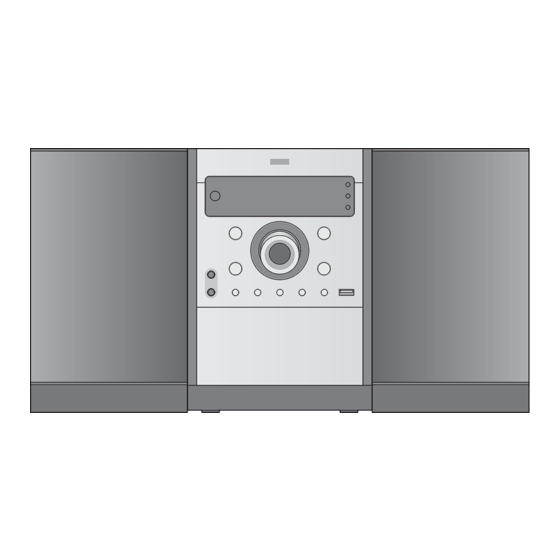
Page 6: Location Of Users Controls
LOCATION OF USERS CONTROLS FRONT / BACK PANEL 1. DISPLAY WINDOW 7. PUSH EJECT position (POWER) (USB connector) PLAY(PAUSE) 9. • (CD SKIP/SEARCH) 4. • (CD SKIP/SEARCH) FAST FORWARD PLAY) FAST REWIND PLAY) • TUNE.+ • TUNE.- 10.VOLUME CONTROL KNOB 5. -
Page 7: Remote Control
REMOTE CONTROL DIMMER POWER MUTE • USB PRESET/FOLDER( • FUNCTION SLEEP VOLUME ( CD FUNCTION CLOCK (PLAY/PAUSE) • PROGRAM/MEMO (CD STOP) • (CD SKIP/SEARCH) • TAPE FUNCTION TUN.-/+ • • (BACKWARD PLAY) REPEAT • • (FORWARD PLAY) D.SKIP • (FAST REWIND PLAY) •... -
Page 8: Specifications
SPECIFICATIONS • GENERAL Power supply Refer to the back panel of the unit. Power consumption Refer to the back panel of the unit. Net Weight 3.4kg External dimensions (WxHxD) 170 x 243 x 282mm • TUNER FM Tuning Range 87.5 ~ 108.0MHz or 65 ~ 74MHz, 87.5 ~ 108.0MHz Intermediate Frequency 10.7MHz Signal to Noise Ratio... - Page 9 MEMO...
-
Page 10: Exploded Views
SECTION 2 EXPLODED VIEWS CABINET EXPLODED VIEW... -
Page 11: Tape Deck Mechanism (Single Deck) Exploded View
TAPE DECK MECHANISM (SINGLE DECK) EXPLODED VIEW... -
Page 12: Cd Mechanism Exploded View
CD MECHANISM (CDM-330) EXPLODED VIEW 012A 012A... -
Page 13: Speaker Exploded View
SPEAKER EXPLODED VIEW MODEL : XCS62F 853R 853L A80L A80R 850R 850L WIRE80 WIRE80... -
Page 14: Packing Accessory View
PACKING ACCESSORY VIEW 808 Battery 824 Antenna Loop (AM) 825 Antenna (FM) 900 Remote Control 801 Instruction Ass'y 803 Packing 803 Packing 804 Bag 802 Box... -
Page 15: Audio Electrical Troubleshooting Guide
SECTION 3 AUDIO PART ELECTRICAL AUDIO ELECTRICAL TROUBLESHOOTING GUIDE 1. POWER (SMPS) No .5.6VA Is the F101 normal? Replace the F101 (Use the same fuse) Is the BD101 normal? Replace the BD101 Is the TH101 normal? Replace the R101 Is Vcc (9V - 18V) Is the D102 normal? supplied to IC101 Pin2? Check or Replace the D102... - Page 16 No 5.0V Is the Vcc(5.6V) Check or Replace the D959 supplied to IC957 pin1? Check the CD CTL “H” Is the IC957 pin4 “H”? signal from µ-com Check or Replace the IC957 No 3.3V Is the Vcc(4.2V) Check or Replace the D943 supplied to IC955 pin1? Check the P CTL “H”...
- Page 17 No -12V Is the voltage 0f Check or Replace the D970 C932 -13V Check the PWR CTL Is the IC155 pin2 “H” signal from µ-com 12V? Check or Replace the Q942 No VF+ Is the ZD950 Replace the ZD950 Normal? Replace the R993 or Q950, Q943...
-
Page 18: Micom Part Check I
2. MICOM PART CHECK I MICOM part check I Refer to Check P-SENS SMPS troubleshooting. (P7904)_PIN6. Check Check the Check both Replace IC101 if input voltage of periphery of IC101 end voltage of IC101 (KIA7042). IC101(KIA7042) is (KIA7042). (KIA7042). over 5V. Check voltage of IC100 Check if IC101(KIA7042) of 78KO/KF2_PIN1. -
Page 19: Micom Part Check Ii
3. MICOM PART CHECK II MICOM part check II Check if Refer to voltage of P7904_PIN5 SMPS troubleshooting. is 5.6V. Check Check if output of both end voltage of D101(RL104) is 5V. D101 Replace D101. Check D101. Check Check if output of IC101 Check Q102_base Q101_ emitter/collector (KIA7042) is over 4.3V. -
Page 20: Ic103(Ks4Cd21Cs) Check
4. IC103(KS4CD21CS) CHECK Check IC100(78KOKF2)_ PIN 22, 24 Refer to PIN22 Check micom micom troubleshooting DATA PIN24 CLK voltage 5V. Replace micom. Check micom. -
Page 21: Fld Display Check
5. FLD DISPLAY CHECK FLD display check Check Refer to SMPS P7904_PIN1, 2, 3 voltage input. Check if both end votage of F1, F2 are over 3.7V. VKK : over 26V. Check WF31 connection and power. Check WF31 connection. Pin1 : FL-22 Pin2 : FL+26 Pin3 : VKK- over 26V. -
Page 22: Pwm Modulation Part Check
6. PWM MODULATION PART CHECK PWM modulation part check Refer to P7905_PIN9 SMPS troubleshooting. 3.3V checking Check X601 Replace X601. Check IC604(PS9829) 12.288MHz. VDD PIN voltage(3, 7, 8, 10, 22, 29, 39, 47, 56, 65, 72, 94). Check X601_PIN2 3.3V. Check Check FB614 Check IC605_... -
Page 23: Power Amp Part Check
7. POWER AMP PART CHECK Power AMP part check P7905_3PIN : +12V, Refer to SMPS troubleshooting. PIN13, 14, 15 : 35V. Check IC700 PIN21, 26, 29, 34 input voltage. Check Check each LINE registor output voltage. IC700 PIN1,17, 18, 19, 36 IC700 : R701, 702, 726, 727 +12V input. -
Page 24: Aux Function Check
8. AUX FUNCTION CHECK AUX function check Check JK800 connection. Check Check IC200(BU4052)_ Check µ-COM(IC301)_ IC200(BU4052)_PIN16 PIN4, 11 input PIN83, 84 commucation. VDD, PIN8 VSS waveform. power. Replace IC200 Check IC200(BU4052)_ PIN3, 13 output waveform. Check Check Refer to IC801(MC4580)_PIN4 IC801(MC4580)_PIN 2, 6 SMPS troubleshooting. -
Page 25: Tuner Function Check
9. TUNER FUNCTION CHECK TUNER function check Check TUNER Check TUNER module voltage(PIN2 : 9V). module(TU601) operation. Check IC200(BU4052)_PIN1, 12 input waveform. Check IC200(BU4052)_PIN3, 13 Check IC200(BU4052)_ output waveform and IC601 PIN16 VDD, PIN8 VSS power. (BU4052)_PIN2,15 input waveform. Replace IC200. Replace IC200. -
Page 26: Tape Function Check
10. TAPE FUNCTION CHECK TAPE function check TAPE PCB ASS`Y Check Check IC200(BU4052)_ IC200(BU4052)_PIN2, 15 input PIN16 VDD, PIN8 VSS power waveform. Replace IC200. Replace IC200. Check IC200(BU4052)_PIN3, 13 output waveform and IC601(BU4052)_ PIN2, 15 input waveform. Check IC200(BU4052)_ Check IC801(MC4580)_ PIN16 VDD, PIN8 VSS power PIN2, 6 input waveform. -
Page 27: Tape Play Part Check
11. TAPE PLAY PART CHECK TAPE PALY part check Check Refer to IC201(HA12237)_PIN16 SMPS troubleshooting. 12V input. Check IC201_ Replace head wire and tape Check PIN5, 26 signal deck mechanism. deck head input. output. Check deck head input IC201_PIN34, 37. Check IC201 Replace IC201. -
Page 28: Tape Rec Part Check
12. TAPE REC PART CHECK TAPE REC part check Check Refer to PWM IC604(PS9829)_PIN49, 52 modulation troubleshooting. PWM output. Check IC201_ PIN7, 24 record input. Check IC201_ Check IC100_PIN23 Replace IC201. PIN10, 21 output. "HIGH" Check Q205(D1304)_ Check L203_PIN2, 3 Check IC100_PIN23 "HIGH"... -
Page 29: Portable In Function Check
13. PORTABLE IN FUNCTION CHECK PORTABLE IN function check Check JK32 connection. Check Check IC200(BU4052)_ Check µ-COM(IC301)_ IC200(BU4052)_PIN16 PIN5, 14 input PIN83, 84 commucation. VDD, PIN8 VSS waveform. power. Replace IC200 Check IC200(BU4052)_ PIN3, 13 output waveform. Check Check Refer to IC801(MC4580)_PIN4 IC801(MC4580)_PIN 2, 6 SMPS troubleshooting. -
Page 30: Internal Block Diagram Of Ics
INTERNAL BLOCK DIAGRAM OF ICs 1. AK5358 AGND VD DGND MCLK Clock Divider Decimation AINL Filter Modulator LRCK SCLK Decimation AINR Filter Modulator Serial I/O SDTO Interface VCOM Voltage Reference CKS2 CKS1 CKS0 2. BU4052 3-16... -
Page 31: Ha12237F
3. HA12237F 3-17... -
Page 32: Lc78692Nw
4. LC78692NW CLOCK DOUT PLL2 EFMIN LRSY GENERATOR Control RFOUT DATACK Audio Output 8FS DIGITAL 1 Bit Control DATA FILTER SLICE DEEMPHASIS PHLPF LEVEL TEST1 Stream CONTROL Control & STDATA ATTENUATION CONTROL STCK DECODER SIGNAL PROCESSOR STREQ Bass-Boost TEST0 Memory I/F MONITOR SLCISET CONT0... -
Page 33: Pt6324
6. PT6324 SG1/KS1 Control SG2/KS2 SG3/KS3 DIN/DOUT SG4/KS4 Serial Data SG5/KS5 Interface SG6/KS6 Display Memory SG7/KS7 SG7/KS7 SG8/KS8 SG9/KS9 SG10/KS10 Timing Generator SG11/KS11 Segment Driver SG12/KS12 SG13/KS13 Key Matrix Memory SG14/KS14 SG15KS15 SG16/KS16 SG17 SG18 LED1 Driver SG19 SG20 SG21 SG22 SG23 SG24... -
Page 34: Tas5142
8. TAS5142 System Microcontroller TAS5508 BST_A Bootstrap Capacitors BST_B RESET_AB VALID RESET_CD PWM_A OUT_A -Order L-C Left- Output Output Filter Input Channel H-Bridge 1 for Each HúBridge 1 OUT_B Output PWM_B Half-Bridge 2-Channel H-Bridge BTL Mode OUT_C PWM_C -Order L-C Output Right- Output Filter... -
Page 35: U1739Ej2V1Ud00/Kf2_E
9. U1739EJ2V1UD00/KF2_E TO00/TI010/P01 16-bit timer/ event counter 00 TI000/P00 Port 0 P00 to P06 RxD6/P14 (LINSEL) TO01/TI011/P06 16-bit timer/ Port 1 P10 to P17 event counter 01 TI001/P05 Port 2 P20 to P27 8-bit timer H0 TOH0/P15 Port 3 P30 to P33 TOH1/P16 8-bit timer H1 Port 4... -
Page 36: Utc Mc4580
10. UTC MC4580 10-1. PIN CONFIGURATION 10-2. TEST CIRCUIT 3-22... - Page 37 MEMO 3-23...
-
Page 38: Wiring Diagram
WIRING DIAGRAM [Total CNT Q'ty : 12ea] 2 CH SPK TERMINAL JACK 1. SMPS MAIN : 2ea 2. MAIN CD : 2ea 3. MAIN FRONT : 2ea SMPS PCB 1 CD SINGLE MD 4. FRONT CD : 1ea 5. CD MD : 3ea 6. -
Page 39: Block Diagram
BLOCK DIAGRAMS 1. SMPS BLOCK DIAGRAM AMP (+) 3 1.5V 3.5V (278R35) 12V (78R12) RECTIFICATION 5V(P-SEN S) SMOOTHING CIRCUIT 5.6VA (KIA278R05) MAIN& PWM IC -12V ZNR & FILTER -31. 5V(VKK) BETWEEN FL1 AND FL2(4.5V) AC INPUT FEED BACK 3-26 3-27... -
Page 40: Main & Front Block Diagram
2. MAIN & FRONT BLOCK DIAGRAM XC102 : 2 CH (50W X 2Ch) W/O DECK XC62 : 2 CH (30W X 2Ch ) W /SINGLE DECK FLD (DISPLAY) VFD DR DRIVE IVE IC XC62 62 ON ONLY PT632 PT6324 DECK/ HD MAIN N BOARD OARD AMP P BOARD... -
Page 41: Schematic Diagrams
BE MODIFIED OR ALTERED WITHOUT PERMISSION FROM THE ACTUAL CIRCUIT USED. THIS WAY, 2. Voltages are DC-measured with a digital voltmeter 1. SMPS SCHEMATIC DIAGRAM FROM THE LG CORPORATION. ALL COMPONENTS IMPLEMENTATION OF THE LATEST SAFETY AND during Play mode. SHOULD... -
Page 42: Main Schematic Diagram
2. MAIN SCHEMATIC DIAGRAM 3-32 3-33... -
Page 43: Amp Schematic Diagram
3. AMP SCHEMATIC DIAGRAM 3-34 3-35... -
Page 44: Deck Schematic Diagram
4. DECK SCHEMATIC DIAGRAM 3-36 3-37... -
Page 45: Front Schematic Diagram
5. FRONT SCHEMATIC DIAGRAM 3-38 3-39... -
Page 46: Printed Circuit Board Diagrams
PRINTED CIRCUIT BOARD DIAGRAMS 1. MAIN P.C.BOARD (TOP VIEW) 3-40 3-41... - Page 47 MAIN P.C.BOARD (BOTTOM VIEW) 3-42 3-43...
-
Page 48: Smps P.c.board
2. SMPS P.C.BOARD 3-44 3-45... - Page 49 3. FRONT P.C.BOARD (TOP VIEW) 3-46 3-47...
-
Page 50: Front P.c.board
FRONT P.C.BOARD (BOTTOM VIEW) 3-48 3-49... - Page 51 MEMO MEMO 3-50 3-51...
-
Page 52: Cd Part Electrical
SECTION 4 CD PART ELECTRICAL CD ELECTRICAL TROUBLESHOOTING GUIDE 1. CD PART TROUBLESHOOTING Turn on CD OPEN CLOSE check Connector check (PN804) Check voltage CN806 PIN1 : 12, PIN2 : 6.3V Check voltage PN805 PIN22 : CLOSE, PIN23 : OPEN Connector check “Reading”... - Page 53 1-1. OPEN CLOSE NG Connector locking check (PN804) Check power supply circuit (PN805, CN806) Defective main power supply CN806 PIN1 : 12V, PIN2 : 6.3V PN805 PIN8 : +5V_AD Check voltage change of OPEN CLOSE IC803 INPUT voltage PIN6 : 12V, Defective micom PIN7:6.3V (PN805 PIN2 : BTL_MUTE, 23 : OPEN,...
- Page 54 1-2. “READING” DISPLAY CHECK (= ONLY “CD” DISPLAY) Conector locking check (PN802, PN804, PN805, CN806) Check power supply port (PN805, CN806) Defective connector or main power supply CN806 PIN1 : 12V, PIN2 : 6.3V, PIN4 : 5V PN805 PIN8 = 5V_AD Check voltage The PIN2 of IC804 Defective IC804...
- Page 55 1-3. READING OK CHECK (= “NO DISC” DISPLAY) Connector locking check (PN801, PN802) Check PN802 Defective pick up or Does sled move? PIN3, 4 (SL+, SL-) IC802 or IC801 Check PN801 Defective pick up or Does lense move? PIN13, 16 (FA+, FA-) IC802 or IC801 (= UP &...
- Page 56 1-4. READING OK CHECK #A (= “NO DISC” DISPLAY) Does Does slin SL+ waveform waveform appear at appear at (IC802 PIN13 (IC802 PIN5) Defective IC801 and PN802 PIN3) waveform #2 waveform #2 sled drive sled motor wave wave Defective IC802 Check PN802 connector line Defective PN802 connector Defective pick up sled motor...
- Page 57 1-6. READING OK CHECK #C (= “NO DISC” DISPLAY) Is 3.3V Is ?V applied applied to to PIN10 of PN801 PIN30, 36, 39, 41, 61, Defective IC804 laser supply voltage 68, 75 of IC801 RF IC check supply voltage check Is 2.3V PIN18 (LDO) of IC801 Defective IC801...
- Page 58 1-7. READING OK CHECK #D (= “NO DISC” DISPLAY) Does Does SP+ waveform spin waveform appear at (IC802 appear at (IC802 PIN6) Defective IC801 PIN11 and PN802 PIN5) waveform #4 waveform #4 spindle spindle drive motor drive wave wave Defective IC802 Check PN802 connector line Defective PN802 connector Defective pick up...
- Page 59 1-8. READING OK CHECK #E (= “NO DISC” DISPLAY) Does Does TA+ waveform tain - waveform appear at (IC802 PIN17 appear at (IC802 PIN22) Defective IC801 and PN801 PIN14) waveform #5 waveform #5 tracking tracking drive coil drive wave wave Defective IC802 Check PN802 Defective PN802 connector...
-
Page 60: Usb Part Troubleshooting
2. USB PART TROUBLESHOOTING Turn on USB “Checking” or Connector check “USB” display check (PN805, CN806, PN810 ) Check power supply circuit (CN806) Check micom interface circuit (PN805) PIN13 : RX (IC805 PIN49 : TXD) PIN14 : TX (IC805 PIN33 : RXD) Reading OK check Check PN810 1PIN : 5V Check PN810 PIN2(D-), 3(D+) -
Page 61: Waveforms Of Major Check Point
WAVEFORMS OF MAJOR CHECK POINT #1.MICOM INTERFACE WAVEFORM #1.MICOM INTERFACE WAVEFORM (PN805 PIN26, 19, 3, 15) during power on (PN805 PIN26, 19, 3, 15) during normal play PIN26 : WRQ PIN26 : WRQ PIN19 : RESET PIN19 : RESET PIN3 : DI (IC801 PIN46 DATA OUT) PIN3 : DI (IC801 PIN46 DATA OUT) PIN15 : DO (IC801 PIN45 DATA IN) PIN15 : DO (IC801 PIN45 DATA IN) -
Page 62: Sled Drive And Motor Waveform
#2.SLED DRIVE AND MOTOR WAVEFORM #2.SLED DRIVE AND MOTOR WAVEFORM (IC802 PIN5, 13) when focus search (IC802 PIN5, 13) during normal play PIN5 : SLIN PIN5 : SLIN PIN13 : SL+ PIN13 : SL+ #3.FOCUS DRIVE AND MOTOR WAVEFORM #3.FOCUS DRIVE AND MOTOR WAVEFORM (IC802 PIN25, IC802 PIN16) (IC802 PIN25, IC802 PIN16) •... -
Page 63: Spindle Drive And Motor Waveform
#4.SPINDLE DRIVE AND MOTOR WAVEFORM #5.TRACK DRIVE AND MOTOR WAVEFORM (IC802 PIN6, 11) when TOC reading (IC802 PIN22, IC802 PIN17) during normal play PIN22 : TAO PIN6 : SPIN PIN11 : SP+ PIN17 : TA+ #6.RF, FOCUS AND TRACKING ERROR WAVEFORM (IC801 PIN2, 10, 16) during normal play PIN2 : RFOUT PIN 16 : TE... -
Page 64: Schematic Diagrams
SCHEMATIC DIAGRAMS 1. CD SCHEMATIC DIAGRAM 4-13 4-14... -
Page 65: Usb Schematic Diagram
2. USB SCHEMATIC DIAGRAM 4-15 4-16... -
Page 66: Printed Circuit Board Diagram
PRINTED CIRCUIT BOARD DIAGRAM CD P.C.BOARD (TOP VIEW) (BOTTOM VIEW) 4-17 4-18... - Page 67 MEMO MEMO 4-19 4-20...