Table of Contents
Advertisement
Advertisement
Chapters
Table of Contents

Related Manuals for Panasonic DMR-ES20P


Summary of Contents for Panasonic DMR-ES20P
-
Page 1: Dvd Video Recorder
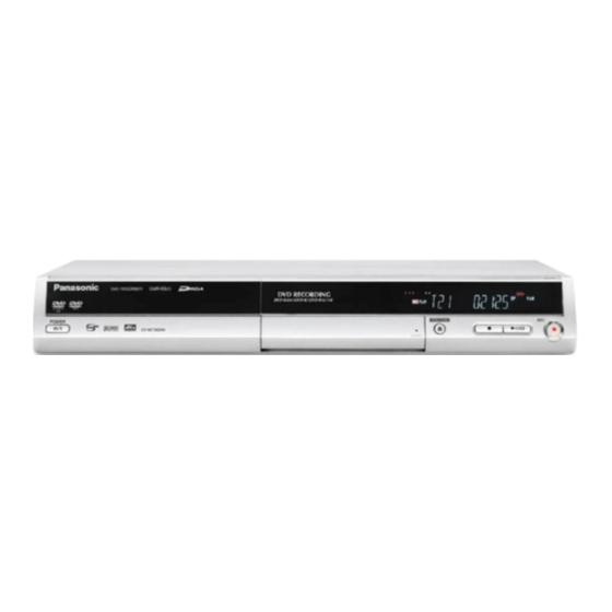
ORDER NO.DSD0508063CE DVD Video Recorder DMR-ES20P DMR-ES20PC Vol. 1 Colour (K).......Black Type (ES20P only) (S).......Silver Type © 2005 Matsushita Electric Industrial Co., Ltd. All rights reserved. Unauthorized copying and distribu- tion is a violation of law. -
Page 2: Table Of Contents
TABLE OF CONTENTS PAGE PAGE 1 Safety Precaution -------------------------------------------------3 1.1. General guidelines -----------------------------------------3 1.2. Caution for fuse replacement ---------------------------3 2 Warning --------------------------------------------------------------4 2.1. Prevention of Electrostatic Discharge (ESD) to Electrostatic Sensitive (ES) Devices ---------------4 2.2. Precaution of Laser Diode -------------------------------5 2.3. -
Page 3: Safety Precaution
1 Safety Precaution 1.1. General guidelines 1. When servicing, observe the original lead dress. If a short circuit is found, replace all parts which have been overheated or damaged by the short circuit. 2. After servicing, see to it that all the protective devices such as insulation barriers, insulation papers shields are properly installed. -
Page 4: Warning
2 Warning 2.1. Prevention of Electrostatic Discharge (ESD) to Electrostatic Sensitive (ES) Devices Some semiconductor (solid state) devices can be damaged easily by static electricity. Such components commonly are called Elec- trostatic Sensitive (ES) Devices. Examples of typical ES devices are integrated circuits and some field-effect transistor-sand semi- conductor "chip"... -
Page 5: Precaution Of Laser Diode
2.2. Precaution of Laser Diode 2.3. Handling the Lead-free Solder 2.3.1. About lead free solder (PbF) Distinction of PbF P.C.B.: P.C.B.s (manufactured) using lead free solder will have a PbF stamp on the P.C.B. Caution: • Pb free solder has a higher melting point than standard solder; Typically the melting point is 50 - 70 F (30 - 40 C) higher. Please use a high temperature soldering iron. -
Page 6: Service Navigation
3 Service Navigation 3.1. Service Information 3.2. Flow chart for confirmation... -
Page 7: Confirm "Ram-Drive Last Error" In Service Mode
3.3. Confirm “RAM-Drive Last Error” in Service Mode Execute Service Mode 1. Press [REC], [CH UP] and [OPEN/CLOSE] simultaneously for 5 seconds when P-off. FL Display: *After finishing display “(9). Factor of Drive Error occurring”, press [0] [2] ~[1] [9] keys of the Remote Controller so that 19 memories can be displayed as maximum. - Page 8 (6) Last Drive Error code No2. (2/2) is displayed for 5 seconds. (7) Error occurring Disc type is displayed for 5 seconds. (8) Unused (No display). (9) Factor of Drive Error occurring is left displayed Error Occurring Disc State...
-
Page 9: Specifications
4 Specifications... -
Page 10: Features
5 Features 5.1. Quick start function(REC) 1. General A few seconds after tuning on the unit,you can start recording to DVD-RAM. You can switch the operation of this function (ON/OFF) on the menu screen. . 2. Quick start (REC) principle In the power-off at Quick start, only power supplies for video IC,tuner and storage media are cut off. -
Page 11: Location Of Controls And Components
6 Location of Controls and Components... -
Page 12: Operation Instructions
7 Operation Instructions 7.1. Taking out the Disc from RAM-Drive Unit when the Disc cannot be ejected by OPEN/CLOSE button 7.1.1. Forcible Disc Eject 7.1.1.1. When the power can be turned off. 1. Turn off the power and press [STOP] [CH UP] keys on the front panel simultaneously for 5 seconds. 7.1.1.2. -
Page 13: Service Mode
8 Service Mode 8.1. Self-Diagnosis and Special Mode Setting 8.1.1. Self-Diagnosis Functions Self-Diagnosis Function provides information for errors to service personnel by “Self-Diagnosis Display” when any error has occurred. U**, H** and F** are stored in memory and held. You can check latest error code by transmitting [0] [1] of Remote Controller in Service Mode. Automatic Display on FL will be cancelled when the power is turned off or AC input is turned off during self-diagnosis display is ON. - Page 14 Error Code Diagnosis contents Description Monitor Display Automatic FL display PLEASE Unit is in termination process Unit is in termination process now. No display WAIT “BYE” is displayed and power will be turned off. In case “Quick Start” of setup menu is ON, it is displayed in restoration operation for AC off.
- Page 15 Item FL display Key operation Mode name Description Front Key Demonstration lock/ Ejection of the disc is prohibited. *When lock the tray. When the power is on, press unlock The lock setting is effective until unlocking the [STOP] and [POWER] keys simulta- tray and not released by “Main unit initializa- neously for 5 seconds.
- Page 16 8.1.3. Service Modes at a glance Service mode setting: While the power is off, press REC, CH UP and OPEN / CLOSE simultaneously for five seconds. Item FL display Key operation Mode name Description (Remote controller key) Release Items Item of Service Mode executing is cancelled. Press [0] [0] or [Return] in service mode.
- Page 17 Item FL display Key operation Mode name Description (Remote controller key) I/P Switch Switch Interlace and Progressive in EE mode. Initial mode is Interlace Press [1] [4] in I/P Switch mode. *Initial setting is “Interlace”. *I/P are switched alternately. *This command is effective during executing “White Picture Output”, “Magenta Picture Out- put”...
- Page 18 Item FL display Key operation Mode name Description (Remote controller key) RAM Drive Last Error RAM Drive error code display. 1. Error Number is displayed for 5 Press [4] [2] in service mode. *For details about the drive error code, refer seconds.
- Page 19 Item FL display Key operation Mode name Description (Remote controller key) S1 signal output Forcibly superimpose the S1 signal (approx. Press [5] [2] in service mode. 4.5V DC) on the EE chroma signal, and check the output on the S terminal. S2 signal output Forcibly superimpose the S2 signal (approx.
-
Page 20: Service Fixture & Tools
9 Service Fixture & Tools Part Number Description Compatibility RFKZ0125 Extension FFC (Digital P.C.B. - DVD-RAM Drive / 40 Pin) Same as E50/ E55/ ES10 series RFKZ0126 Extension Cable (MainP.C.B. - DVD-RAM Drive/ 4 Pin) Same as E30/ HS2/ ES10 series RFKZ0260 Extension Cable (MainP.C.B. -
Page 21: Disassembly And Assembly Instructions
10 Disassembly and Assembly Instructions 10.1. Disassembly Flow Chart The following chart is the procedure for disassembling the casing and inside parts for internal inspection when carrying out the servicing. To assemble the unit, reverse the steps shown in the chart below. 10.2. -
Page 22: Top Cover
10.3. Top Cover 10.5. Digital P.C.B. 1. Remove the 2 Screws (A) and 3 Screws (B). 1. Remove FFC and 3 Screws (A). 2. Slide Top Cover rearward and open the both ends at rear 2. Lift up Digital P.C.B. slightly so to disconnect 2 Connec- side of the Top Cover a little and lift the Top Cover in the tors to remove Digital P.C.B. -
Page 23: Dv Javk P.c.b
10.5.1. Removing and attaching Heart Sink 10.6. DV Javk P.C.B. Unit for IC5001 1. Remove 2 Screws (A) to remove SD Card Angle with DV Jack P.C.B. 10.7. DVD-RAM Drive (Removing) 1. Push Rivets by finger as shown below. 1. Remove 3 Screws (A) to remove DVD-RAM Drive. 2. -
Page 24: Rear Panel & Fan Motor
10.8. Rear Panel & Fan Motor 10.8.2. Only Fan Motor 1. Disconnect Fan Connector. 10.8.1. Rear Panel with Fan Motor 1. Disconnect Fan Connector. 2. Remove 2 Screws (A) to Remove Fan Motor. 2. Remove 5 Screws (A) and 1 Screw (B). 3. -
Page 25: Main P.c.b
10.9. Main P.C.B. 1. Disconnect Connector (A) for Front (L) P.C.B. 2. Remove 4 Screws (A). 3. Remove Digital P.C.B. Angle to remove Main P.C.B. 10.10. Front (L) P.C.B. 1. Remove 2 Screws (A). 2. Front (L) P.C.B. is removed in the direction of the arrow. -
Page 26: Measurements And Adjustments
11 Measurements and Adjustments 11.1. Service Positions Note: For description of the disassembling procedure, see the section 10. 11.1.1. Checking and Repairing of Digital P.C.B. - Page 27 11.1.2. Checking and Repairing of Main P.C.B.
- Page 28 11.1.3. Checking and Repairing of DVD-RAM Drive...
-
Page 29: After Replacing The Ram Drive With New One
Perform auto recording and playback for one minute using the RAM No abnormality should be seen in the picture, sound or operation. disc. *Panasonic DVD-RAM disc should be used when recording and playback. If a problem is caused by a VCD, DVD-R, DVD-Video, Audio-CD, or No abnormality should be seen in the picture, sound or operation. -
Page 30: Miscellaneous
12 Miscellaneous 12.1. Abbreviations INITIAL/LOGO ABBREVIATIONS ERROR TORQUE CONTROL INITIAL/LOGO ABBREVIATIONS ERROR TORQUE CONTROL REFER- A0~UP ADDRESS ENCE ACLK AUDIO CLOCK ENCSEL ENCODER SELECT AD0~UP ADDRESS BUS ETMCLK EXTERNAL M CLOCK (81MHz/40.5MHz) ADATA AUDIO PES PACKET DATA ETSCLK EXTERNAL S CLOCK (54MHz) ADDRESS LATCH ENABLE FBAL FOCUS BALANCE... - Page 31 INITIAL/LOGO ABBREVIATIONS INITIAL/LOGO ABBREVIATIONS READ ENABLE VBLANK V BLANKING RFENV RF ENVELOPE COLLECTOR POWER SUPPLY RF PHASE DIFFERENCE OUTPUT VOLTAGE (CD-ROM) REGISTER SELECT VCDCONT VIDEO CD CONTROL (TRACKING RSEL RF POLARITY SELECT BALANCE) RESET DRAIN POWER SUPPLY VOLTAGE RESERVE VIDEO FEED BACK VREF VOLTAGE REFERENCE SBI0, 1...
- Page 32 DVD Video Recorder when there is no specify mode is mentioned. DMR-ES20P 4.Although the voltage and waveform available on here is measured with standard frame, it may be differ from actual measurement due to modification of circuit and so on.
-
Page 33: S2. Voltage And Waveform Chart
S2. Voltage and Waveform Chart S2.1. Main P.C.B. <IC1150> <IC3001> REF No. PIN No. REC REF No. PIN No. REC REF No. PIN No. REC REF No. PIN No. REC IC3001 IC3001 IC7501 IC1150 IC3001 IC3001 IC7501 IC1150 IC3001 IC4001 IC7501 IC1150 IC3001... -
Page 34: S2.2. Dv_Jack P.c.b
S2.2. DV_Jack P.C.B. <P7401> REF No. PIN No. REC REF No. PIN No. REC REF No. PIN No. REC REF No. PIN No. REC IC7505 P7401 IC7801 IC7801 IC7505 P7401 IC7801 IC7801 IC7505 P7401 IC7801 IC7801 IC7505 P7401 IC7801 IC7801 IC7505 P7401 IC7801... -
Page 35: S3. Block Diagram
IC1302 (REG.DR+5V) DR+5V P1501 P102 VOUT (TO DVD RAM DRIVE) IC1200 (SHUNT REG.) Q1200 DR POWER ON IC7501- PHOTO COUPLER IC1503 (JC.REG.+5V) JC REG +5V VOUT JC POWER ON IC7501- IC1502 (REG.D+5V) D+5V COLD VOUT DMR-ES20P/PC Power Supply Block Diagram... -
Page 36: S3.2. Power Supply Block Diagram (2
TUNER P.C.B. T7501 IR7501- 3 IP7501 (POWER TRANS.) UNREG+38V PP7404 PS7801 TU7801- JC REG +5V JC REG+5V PP7404 PS7801 TU7801- IC7801- IC3001(+5V) IC7404- 8 D+5V D+5V P7401 P6001 IC5001/IC6006(+5V) IC4901- 2 DMR-ES20P/PC DMR-ES20P/PC Power Supply Block Diagram Power Supply Block Diagram... -
Page 37: S3.3. Analog Video Block Diagram
TO DIGITAL VIDEO2 IN LINE 2V IN Q3002 BLOCK SECTION VIDEO IN CLAMP COUT A CPNCIN DM P7401 P6001 CPN 2C IN C2 IN BIAS Y2 IN CPN 2Y IN CLAMP C/S DET2 S-VIDEO C/S DET2 DMR-ES20P/PC Analog Video Block Diagram... -
Page 38: S3.4. Analog Audio Block Diagram
A/V OUT JACK P6001 P7401 IECOUT MIX L OUT2 OUT-L LINE XTMUTE IC7501- Q4003 MIX R OUT2 MUTE OUT-R QR4001,4002 QR4003 Q4002 FROM DIGITAL P.C.B. P6001 P7401 XDMUTE (5V) MUTE MUTE MUTE AUDIO NET SECTION DMR-ES20P/PC Analog Audio Block Diagram... -
Page 39: S3.5. Analog Timer Block Diagram
IC7505 (FAN MOTOR DRIVE) X SW +12.5V Q7504 FAN PWM (FAN MOTOR DRIVE) TO AUDIO XT MUTE XT MUTE BLOCK SECTION FAN MOTOR P7503 P7503 FROM VIDEO FAN LOCK L1 SWIDE L123 SWIDE BLOCK SECTION DMR-ES20P/PC Analog Timer Block Diagram... -
Page 41: S4. Schematic Diagram
S4. Schematic Diagram S4.1. Interconnection Diagram DMR-ES20P/PC Interconnection Diagram P7503 FAN2OUT P1101 FAN2LOCK P7502 KEYIN3 RAM DRIVE S-10 S-10 VXY1867 DIGITAL... - Page 42 DMR-ES20P/PC Interconnection Diagram TU7801 ENGF6503GRF AUDIO IN CH SW REG5V TV/VCR VIDEO IN PP7404 PS7801 X_SW_5R8V JC_REG_5V JC_P_ON_H IIC_CLK IIC_CLK IIC_DATA IIC_DATA IF OUT UNREG_38V UNREG_38V TUNER_VIDEO1 TUNER_VIDEO1 AFTOUT 1TUNER_R 1TUNER_R (US) 1TUNER_L 1TUNER_L AUDIOOUT SIFOUT TUNER BTL+30VIN VJB07A76(A,B,C,D E,F,G,H,J)
- Page 43 DD14 DGND DGND DD13 DD13 P_OFF_L XFWE DD12 DD12 DGND XMPREQ DD11 DD11 SBMTP SBPTM DD10 DD10 XINTM SCLK XINTP I2C5CK /HRST RESET- P102 P1501 DR5V DRGND MGND DR12V DR12V FRONT L DV JACK VJB70124 VJB73132 DMR-ES20P/PC Interconnection Diagram S-12...
- Page 44 XFWE AU5V XFWE AU5V DGND XDMUTE DGND XDMUTE XMPREQ DGND XMPREQ DGND SBMTP DGND SBMTP DGND SBPTM DGND SBPTM DGND XINTM DGND XINTM DGND SCLK SCURVE1 SCLK SCURVE1 XINTP SCURVE0 XINTP SCURVE0 I2C5CK I2C5DT I2C5CK I2C5DT DMR-ES20P/PC Interconnection Diagram S-13...
-
Page 45: S4.2. Av_I/O(A) Schematic Diagram
S4.2. AV_I/O(A) Schematic Diagram DMR-ES20P/PC AV_I/O Section (Main P.C.B.(1/3)) Schematic Diagram(A) R4003 R4004 LB7410 P7401 LB7409 J0JHC0000032 K1KA88A00002 J0JHC0000032 I2C5DT I2C5CK SCURVE0 XINTP SCURVE1 SCLK DGND XINTM DGND SBPTM DGND SBMTP DGND XMPREQ XDMUTE DGND AU5V XFWE DGND P_OFF_L DGND... - Page 46 DMR-ES20P/PC AV_I/O Section (Main P.C.B.(1/3)) Schematic Diagram(A) R4003 100K R4004 100K C4018 C4019 C4024 F2A1E470A205 R4033 R4037 Q4002 2SD0601A0L R4034 X_SW_5R8V R4035 X_SW_12V Q4003 2SD0601A0L R4032 IC4901 B3ZAZ0000016 C4025 F2A1E470A205 C4903 C4904 R4036 R4038 K4003 F2A0J470A599 0.1[ZF] VWJ0795=5 C4012 F2A1E470A205...
- Page 47 [23]S1/S R3005 LB4911 J0JCC0000103 C3007 C OUT B [78]DVCC2 [22]DRV Q3002 [79]BLSW OUT [21]Y 3 SW GND1 B1ABCF000020 R3030 [80]TEST3 BL SW IN LB4912 J0JCC0000103 R3006 R3008 R3007 R3032 C3020 0.01 L123_SWIDE DMR-ES20P/PC AV_I/O Section (Main P.C.B.(1/3)) Schematic Diagram(A) S-16...
- Page 48 [78]DVCC2 [22]DRV GND2 Y75 OUT [79]BLSW OUT [21]Y 3 IN SW GND1 DRV VCC1 R3030 [80]TEST3 BL SW IN C 3 IN C3012 0.01 C3034 0.01 R3036 L3001 G0C220JA0019 R3032 C3020 0.01 DMR-ES20P/PC AV_I/O Section (Main P.C.B.(1/3)) Schematic Diagram(A) S-17...
-
Page 49: S4.3. Power Section(P) Schematic Diagram
S4.3. Power Section(P) Schematic Diagram DMR-ES20P/PC Power Section (Main P.C.B.(2/3)) Schematic Diagram(P) LB1281 L1280 G0A220GA0026 J0JKB00000 CAUTION: FOR CONTINUED PROTECTION AGAINST FIRE HAZARD, REPLACE ONLY WITH THE SAME TYPE 1.6A 250V FUSE. LB1280 D1280 ATTENTION: POUR UNE PROTECTION CONTINUE LES RISQUES... - Page 50 DMR-ES20P/PC Power Section (Main P.C.B.(2/3)) Schematic Diagram(P) K1281 VWJ0795=17.5 X_SW_3R2V X_SW_5R2V IP1400 LB1281 D1281 L1280 K5H302100004 B0JCPE000015 G0A220GA0026 J0JKB0000003 D1280 B0JAQE000004 L1401 K1401 C1402 G0A100ZA0041 ERJ3GEY0R00V 0.01 LB1401 J0JHC0000032 D1R8V DDGND FAN_GND K1502 ERJ3GEY0R00V IP1270 K5H302100004 X_SW_5R8V LB1271 L1270 G0A100HA0023...
- Page 51 R1151 R1152 7500 D1152 MAZ4130NMF D1153 MA2C165001VT Q1200 R1155 R1156 B3PBA0000237 C1153 R1209 R1207 6800 2200P 1K[D] 240[D] C1202 R1208 C1200 2200[D] ECQV1H224JL3 0.22[V] IC1200 #C0DAEMB00003 ZA1103 K9ZZ00001279 ZA1104 K9ZZ00001279 C1504 F1H1A105A028 DMR-ES20P/PC Power Section (Main P.C.B.(2/3)) Schematic Diagram(P) S-20...
- Page 52 C1303 C1302 F2A1A2210063 $(0.1) D1300 10V220[JF] $[B0JCPE000015] C1200 ECQV1H224JL3 0.22[V] D1502 D1503 D1504 B0JCPE000015 B0JCPE000015 B0JCPE000015 JC_REG5V JC_P_ON_H K1505 D3R3V $[VWJ0795=5] IC1503 C0CBCDG00006 (PQ050DNA1ZPH) ANA3R3V D1506 R1506 MA2C165001VT C1504 C1514 F1J0J106A014 F1H1A105A028 DMR-ES20P/PC Power Section (Main P.C.B.(2/3)) Schematic Diagram(P) S-21...
-
Page 53: S4.4. Timer Section(T) Schematic Diagram
S4.4. Timer Section(T) Schematic Diagram DMR-ES20P/PC Timer Section (Main P.C.B.(3/3)) Schematic Diagram(T) DP7501 A2BD00000127 (4-MT-233NK) CL7507 CL7506 R7537 R7538 R7539 R7540 R7531 R7535 XINTM 5VDET XMPREQ C7517 $(0.01) XINTP CL7504 IC7503 C0EBJ0000110 R7518 SEG9 SYNCDET R7527 100K R7541 SEG10 TEST2... - Page 54 DMR-ES20P/PC Timer Section (Main P.C.B.(3/3)) Schematic Diagram(T) R7546 D7506 LB7501 K7503 ERDS2TJ1R0T B0AAGM000007 ERJ3GEY0R00V ERJ3GEY0R00V Q7501 $[2SD132800L] R7543 $(10K) QR7501 $[UNR511300L] D7508 LB7504 B0AADM000003 ERJ3GEY0R00V C7533 F2A1H100A820 LB7502 D7507 LB7503 VWJ0023=5 B0AADM000003 ERJ3GEY0R00V T7501 C7532 G4D1A0000115 F2A1V470A654 DDGND R7551 C7531...
- Page 55 OP-CMD XRESET P7502 R7521 R7522 K1KB04AA0063 2700 5600 OPEN/CLOSE S7501 CH UP PLAY EVQPC105K S7503 S7504 EVQPC105K EVQPC105K KEYIN3_POWER R7525 R7523 2700 2200 CH DOWN STOP S7506 S7507 S7505 EVQPC105K EVQPC105K EVQPC105K DMR-ES20P/PC Timer Section (Main P.C.B.(3/3)) Schematic Diagram(T) S-24...
- Page 56 C7536 (C0EBE0000247) $(0.01) R7554 $(47K) QR7502 D3R3V $[UNR521200L] R7555 C7534 $(15K) $(0.01) X_SW_12V R7556 C7540 1u[ZF] C7542 0.1[ZF] Q7504 B1ABMD000004 TO REAR PANEL FAN P7503 R7557 K1KA03AA0192 R7558 FANDCOUT R7559 FANLOCK FAN_GND DMR-ES20P/PC Timer Section (Main P.C.B.(3/3)) Schematic Diagram(T) S-25...
-
Page 57: S4.5. Tuner Pack Schematic Diagram
J0B4504A0029 EFCT4R5MS5W EFCT4R5MS5W IC7801 $[AN5832SA-E1V] AN5832SA-E1V AN5832SA-E1V IC7802 AN5833SA-E1V $[AN5833SA-E1V] AN5833SA-E1V K7801 $[ERJ6GEY0R00V] ERJ6GEY0R00V ERJ6GEY0R00V PS7801 K1KB13B00013 K1KB13B00013 K1KB20B00027 R7801 R7803 3300 3300 DMR-ES20P/PC R7807 180K 180K Tuner Pack R7812 ERDS2TJ102T ERDS2TYJ102T ERDS2TYJ102T Schematic Diagram TU7801 ENGF4506GRF ENGF6503GRF ENGF6502GF S-26... -
Page 58: S4.6. Dv_Jack Schematic Diagram
S4.6. DV_Jack Schematic Diagram / S4.7. Front_L Schematic Diagram POWER P37001 P7001 P37002 S7001 K1KA06B00181 K2HZ104B0012 K1KA04A00394 EVQPC105K (IMSA-9850B-06Z900) (IMSA-9390S-04Z901) TPA+ TPA+ KEYIN3_POWER TPA- TPA- TPB+ TPB- TPB+ TPB- DMR-ES20P/PC DMR-ES20P/PC DV_Jack Front_L Schematic Diagram Schematic Diagram S-27... -
Page 59: S5. Print.circuit.board
S5. Print.Circuit.Board. S5.1. Main P.C.B. S5.1.1. Main P.C.B.(Compornent Side) / S5.1.2. Main P.C.B.(Foil Side) DMR-ES20P/PC Main P.C.B. R1155 R1156 C1202 R1209 S-28 S-28 R1207 R1208 R1202... - Page 60 DMR-ES20P/PC Main P.C.B. C4906 R4901 C4027 R3909 R4038 R4037 C4026 R4903 C4904 R3911 R3907 R3923 C7541 R3902 LB4901 R4033 IC7505 R7559 K7505 R4003 R4004 R4008 R4011 R4012 C3020 C3043 W507 C3011 C3014 W517 C7542 W509 C3034 C4010 R3036 C3010 C4011...
- Page 61 C1202 R1209 R1207 R1208 R1202 C1502 R754 R7549 (Component Side) DMR-ES20P/PC Main P.C.B. S-30...
- Page 62 R7516 D1400 R7515 CL7501 R7536 C1302 R7514 K1401 LB7505 CL7504 R7527 IC7501 TL7502 R7560 R7551 R7506 R7553 R7505 C7543 LB7504 CL7507 W511 R3927 CL7506 C3902 C3901 R7537 R7535 R3928 R3929 R3926 LB4912 LB3929 R7521 (Foil Side) DMR-ES20P/PC Main P.C.B. S-31...
-
Page 63: S5.1.3. Main P.c.b. Address Information
S5.1.3. Main P.C.B. Address Information Main P.C.B Integrated Circuit P7503 L1280 C1281 C3043 J-19 C7510 E-18 R1507 G-19 R4901 L-16 R7552 D-13 IC1150 PP7404 L1301 C1300 E-19 C3044 C7511 E-18 R3001 I-19 R4903 L-16 R7553 D-13 IC1200 G-10 L1400 C1301 E-19 C3046 I-20... -
Page 64: S5.2. Dv_Jack P.c.b
S5.2. DV_Jack P.C.B. (Component Side) (Foil Side) DMR-ES20P/PC DV_Jack P.C.B. S-33... -
Page 65: S5.3. Tuner Pack P.c.b
S5.3. Tuner Pack P.C.B. C7822 C7827 C7828 LB7805 W515 W511 W512 R7810 C7826 W513 R7803 C7809 C7813 W503 C7818 IC7801 W502 R7808 IC7802 R7809 R7802 C7819 W504 W518 C7803 W510 W507 W505 W519 (Component Side) (Foil Side) DMR-ES20P/PC Tuner Pack P.C.B. S-34... -
Page 66: S5.4. Front_L P.c.b
S5.4. Front_L P.C.B. (Component Side) (Foil Side) DMR-ES20P/PC Front_L P.C.B. S-35... - Page 67 S-36...
-
Page 68: S6. Replacement Parts List
S5. Replacement Parts List Note: 1.* Be sure to make your orders of replacement parts according to this list. 2. IMPORTANT SAFETY NOTICE Components identified with the mark have the special characteristics for safety. When replacing any of these components, use only the same type. 3. - Page 69 S-38...
- Page 70 S-39...
- Page 71 S-40...
- Page 72 S-41...
- Page 73 DMR-ES20P-S M1 / M2 Ref.No. Part No. Part Name & DescriptionPcs Remarks Ref.No. Part No. Part Name & DescriptionPcs Remarks RMX0335 DRIVE CUSHION RPG7660 PACKING CASE 1 (PK) RMZ0784 INSULATION SHEET RPG7661 PACKING CASE 1 (PCS) RMC0654 SPRING RPN1817-1 CUSHION VEP70124A FRONT(L)P.C.B.
-
Page 74: S7. Exploded Views
S7. Exploded Views S7.1. Frame & Casing Section 20-1 1 (RTL) TUNER P.C.B. DRIVE P.C.B. 3 (RTL) DIGITAL P.C.B. DRIVE P.C.B. 24 (RTL) DV JACK 2 (RTL) P.C.B. MAIN P.C.B. 17 (RTL) FRONT (L) P.C.B. 12-2 12-4 12-5 12-8 12-6 12-1 12-7 12-3... -
Page 75: S7.2. Packing Parts & Accessories Section
S7.2. Packing Parts & Accessories Section BATTERY (REMOTE CONT.) A1-1 S-44...