Table of Contents
Advertisement
SERVICE MANUAL
DP65 & DP65G
N N T T S S C C
SERVICE MANUAL REVISION HISTORY INFORMATION
DATE
Mar , 06
4.27.06
08.03.06
08.04.06
08.09.06
SPECIFICATIONS AND PARTS ARE SUBJECT TO CHANGE FOR IMPROVEMENT
PROJECTION COLOR TELEVISION
MARCH 2006
C C h h a a s s s s i i s s
REVISON #
SM00001
FIRST ISSUE OF MANUAL
REVISION 2
SM00002
PART NUMBERS CORRECTED
CH 1
CH 2
PARTS LIST REVISED
CH 3
PART NUMBERS ADDED
HHEA-MANUFACTURING DIVISION
No. 0216
PA
51F59 DP65 51F59A/J DP65G
57F59 DP65 57F59A/J DP65G
65F59 DP65 65F59A/J DP65G
R/C: CLU-4361S
REASON
Advertisement
Table of Contents

Related Manuals for Hitachi 57F59A


Summary of Contents for Hitachi 57F59A
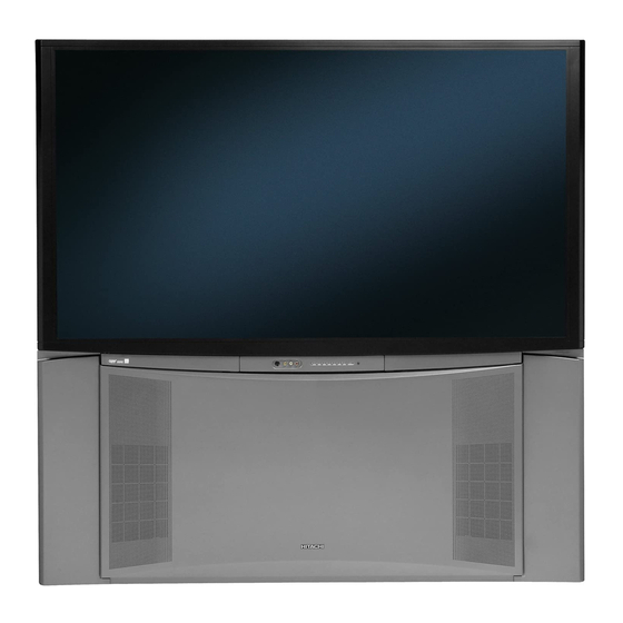
- Page 1 No. 0216 51F59 DP65 51F59A/J DP65G 57F59 DP65 57F59A/J DP65G SERVICE MANUAL 65F59 DP65 65F59A/J DP65G DP65 & DP65G N N T T S S C C R/C: CLU-4361S C C h h a a s s s s i i s s...
-
Page 2: Table Of Contents
No. 0216 51F59 DP65 51F59A/J DP65G 57F59 DP65 57F59A/J DP65G SERVICE MANUAL 65F59 DP65 65F59A/J DP65G DP65 & DP65G N N T T S S C C R/C: CLU-4361S C C h h a a s s s s i i s s... -
Page 3: Important Safety Instructions
Before servicing this chassis, it is important that the service technician read and follow the “Important Safety Instructions” in this Service Manual. For continued X-Radiation protection, replace picture tube with original type or Hitachi approved equivalent type. This Service Manual is intended for qualified service technicians; it is not meant for the casual do-it-yourselfer. -
Page 4: Important Safety Instruction
DP65 IMPORTANT SAFETY INSTRUCTION 1. Before returning an instrument to the customer, always make a safety check of the entire instrument, including but not limited to the following items. (READING SHOULD NOT a. Be sure that no built-in protective devices are LEAKAGE BE ABOVE 0.5MIU) defective and/or have been deleted during servicing. -
Page 5: Important Safety Instructions
For continued X-radiation protection, the replacement making test measurements. tube must be the same type as the original, Hitachi 2. To prevent X-radiation, after replacement of approved type. picture tube and lens, confirm these components... - Page 6 4. Picture Tube Implosion Protection Warning – The safety characteristics as the recommended replace- picture tube in this receiver employs integral ment part in Hitachi service data parts list might implosion protection. For continued implosion create shock, fire, and/or other hazards. Product...
-
Page 7: Servicing Precautions
DP65 SERVICING PRECAUTIONS CAUTION: Before servicing instruments covered by this 7. Do not apply AC power to this instrument and/or any of its service data and its supplements and addenda, read and electrical assemblies unless all solid-state device heat- follow the “Important Safety Instructions” on page 3 of this sinks are correctly installed. - Page 8 Use Solding Iron to Pry Leads 4. Securely crimp each connection and solder it. IC Removal/Replacement Some Hitachi unitized chassis circuit boards have slotted 5. Inspect (on the circuit board copper side) the solder joints holes (oblong) through which the IC leads are inserted and of the two “original leads”.
- Page 9 2. Trace along the copper pattern from both wire sides of ensure the maintenance of reliability and safety standards, the pattern break and locate the nearest component contact your Hitachi personnel. directly connected to the affected copper pattern. At IC Connections 3.
- Page 10 DP65 SERVICING PRECAUTIONS NOTE: These components are affixed with glue. Be careful not to break or damage any foil under the component or at the pins of the ICs when removing. Usually applying heat to the component for a short time while twisting with tweezers will break the component loose.
- Page 11 DP65 Information for service about lead-free solder introduction Hitachi introduced lead-free solder to conserve the "Earth Environment". Please refer to the following before servicing. (1) Characteristic of lead-free solder Melting point of lead free solder is 40-50 C higher than solder containing lead.
-
Page 12: Technical Cautions
DP65 TECHNICAL CAUTIONS CAUTIONS WHEN CONNECTING / DISCONNECTING THE HV CONNECTOR Perform the following when the HV connector (anode connector) is removed or inserted for CPT replacement, etc. Anode connector Deflection P.W.B. During Removal Roll out silicon cover from FBT’s contact area slowly. While turning the connector about 90 degrees following the arrow (0 position), push the connector PUSH... - Page 13 DP65 TECHNICAL CAUTIONS High Voltage limiter circuit operation check. 4. When the limiter circuit is operating properly, High 1. Turn off TV and connect jig as shown in Figure 2. Adjust Voltage will be less than 37 kV at 1.62mA when TV shuts jig fully counter-clockwise for minimum resistance.
-
Page 14: Specifications
SPECIFICATIONS Intermediate Frequency: Picture l-F Carrier 45.75 MHz Models: 51F59/A/J 57F59/A/J 65F59/A/J Sound l-F Carrier 41.25 MHz Cathode-Ray Tube: Color Sub Carrier 42.17 MHz 51F59A/J,57F59A/J,65F59A/J 51F59,57F59,65F59 R=P16LXL00RFA R=P16MAB00RFA Video Input: 1 Volt p-p, 75 Ohm G=P16LXL00HHA G=P16MAB00HHA B=P16LXL00BMB B=P16MAB00BMB Video Output:... - Page 15 DP65 Feature Spec. Differences Sheet Items 51F710A 51F59/A 57F59/A 65F59/A 51F59J 57F59J 65F59J Screen Size(WxH) 51" 1129x635 <- 57" 1262x710 65" 1439x809 51" 1129x635 57" 1262x710 65" 1439x809 Aspect Ratio 16:9 <- <- <- <- <- <- 1239x1275x557 <- 1372x1386x599 1549x1521x708 1239x1275x557 1372x1386x599 1549x1521x708 Set Diimension(WxHxD)...
-
Page 16: General Information
DP65 GENERAL INFORMATION POWER º ´ · ³ ² ¿ ¶ ³ MENU/SELECT button ´ POWER button/ POWER LED Press this button to turn the TV on or off. This LED This button allows you to enter the MENU, making it possible to set TV features to your preference light is on during normal operation. -
Page 17: Audio Out
DP65 GENERAL INFORMATION ´ ² ¿ ³ ¶ º » · ¾ ³ AIR /CABLE Input NOTE: 1. Do not connect composite VIDEO and CABLE – A 75-Ohm RF antenna or CATV (Cable S-VIDEO to INPUT 1, 2 or 5 at the same TV) input. - Page 18 NOTE : This OUTPUT is for DIGITAL channels only. º Upgrade Card This card slot is for future software upgrades. Hitachi will notify you if a software upgrade is required for your TV. In order to receive written notification, please complete and return your warranty card.
- Page 19 DP65 GENERAL INFORMATION TIPS ON REAR PANEL CONNECTIONS External Digital • S-VIDEO, Y-P and HDMI Component connections are provided for with HDMI output high performance laserdisc capability players, VCRs etc. that have this feature. Use these HDMI OUT connections in place of the standard video connection if your device has this feature.
- Page 20 DP65 GENERAL INFORMATION Connecting External Audio Sources Match the numbers below to the diagram for speaker placement. ³ The television’s internal speakers will act as center speaker (select AUDIO - INTERNAL SPEAKERS - TV AS CENTER). · These FRONT left and right speakers are connected to the FRONT output of a separate audio amplifier.
- Page 21 DP65 Front Panel Jacks and Connections The front panel jacks are provided as a convenience to allow you to easily connect a camcorder or VCR as shown in the following examples: NOTE: 1. Completely insert connection cord plugs when connecting to front panel jacks. If you do not, the played back picture may be abnormal.
- Page 22 Quick Guide for the Remote Control In addition to controlling all of the functions on your HITACHI Projection TV, the new remote control is designed to operate different types of devices, such as, DVD Players, CBL (Cable Boxes), set-top-boxes, satellite receivers, and VCRs.
- Page 23 DP65 DISPLAY PICTURE FORMAT ´ ASPECT button Press this button to quickly change the picture format ASPECT ratio. Depending on the input signal format received, the picture format ratio allows you to adjust the images through the following options. 4:3 STANDARD 4:3 ZOOM1/ZOOM2 Use this aspect mode to display conventional (4:3) Use these aspect modes to zoom in on...
- Page 24 DP65 Picture-in-Picture (PIP) Your HITACHI Projection TV incorporates one Tuner technology designed for improved viewing enjoyment. This Tuner feature allows you to view antenna input on the main picture and a Video Input on sub-picture simultaneously. When an ANALOG channel or INPUT is viewed as the main picture, an ANALOG channel or INPUT can not be viewed as a sub picture.
- Page 25 DP65 Picture-in-Picture (PIP) · PAUSE button PIP Mode Picture-in-Picture This feature is only available with a 1080i If you wish to freeze the sub-picture, press the signal. To prevent a pattern burn, occasionally PAUSE button. This is convenient when trying to move the sub-picture using the CURSOR write down the address for a mail order company, buttons.
- Page 26 DP65 Picture-in-Picture (PIP) MAIN FREEZE STROBE FREEZE Press the PAUSE button to freeze one frame of the Press the PAUSE button to freeze three frames of picture you are currently viewing and the frozen the picture you are currently viewing (only the 3 frame will show in the Main Picture.
- Page 27 DP65 Picture-in-Picture (PIP) PIP Specifications PIP Inp ut Mode Cable Input1 Input2 Input3 Input4 Input5 Sub Picture Digital CH Digital CH HDMI S/Video S/Video Ypbpr Ypbpr S/Video Main Picture Analog CH Analog CH Video Video Digital CH Analog CH Cable Digital CH Analog CH Input1...
- Page 28 DP65 Picture-in-Picture (PIP) PIP Specifications (cont.) SPLIT Mode Scan Aspect Digital CH Analog 1080i 720p 480p 480i S/Video Mode 480i 16x9 16x9 16x9 16x9 16x9 16x9 Main £- £- 540p Digit al CH 16x9 £- (480i) £- Analog CH £- £- 1080i 16x9...
- Page 29 (MMC CARD). If a Set Black Side Panel future software upgrade is required for your TV, Set Closed Captions HITACHI will notify and provide you with a flash card. Set Audio Out Upgrades In order to receive written notification and the flash Move card, please complete and return the warranty card.
-
Page 30: Service Adjustments
NTSC (480i) signal generator. Hitachi recognizes that few companies offer HDTV or SDTV signal generators and that the cost of these generators is sometimes prohibitive. For this reason, we suggest the use of a set-top-box for HDTV and SDTV adjustments. Usually, there is a switch on the set-top-box which enables it to output HDTV (1080i or 720P) or SDTV (480P) signals even with no input. - Page 31 When the PTV set is in adjustment mode, the cursor and MENU keys of the remote control or front panel may be used as the adjustment keys. A. Use any Hitachi remote control when making an adjustment. ·Process of Memory Initialize operation.
- Page 32 DP65 2.0 FINAL ADJUSTMENT ORDER FOR SERVICE ORDER ADJUSTMENT ITEM ASPECT MODE SIGNAL DATA CUT OFF 16:9 Standard NTSC Signal PREFOCUS 16:9 Standard Crosshatch DCU PHASE DATA SETTING 16:9 Standard NTSC Signal-DCU HORIZONTAL POSITION 16:9 Standard Circle Pattern ADJUSTMENT (COARSE) RASTER TILT 16:9 Standard NTSC Signal-DCU...
- Page 33 DP65 1.3 Comb filter operation check Important: High Voltage adjustment should Adjustment preparation NOT be adjusted in field. This is (1) Receive the color bar signal at the regular tuning adjusted at factory using precise point. loads should (2) Set the CONTRAST control to MAX and the other readjusted.
- Page 34 DP65 Adjustment procedure Adjustment procedure Press the MENU key on the CONTROL PANEL of (1) Receive circle pattern. the TV, then press the R/C keys MENU+8+SELECT (2) Push SERVICE ONLY switch to display DC to enter adjustment mode. crosshatch. Mark the DC crosshatch center position using your finger tip.
- Page 35 DP65 (4) Turn the deflection yoke of R or B and set so that the 2.6 Raster position adjustment inclination of R or B light with respect to the green Adjustment preparation light is as shown below on the top and bottom sides. (1) The set can face east or west.
- Page 36 DP65 2.7 Beam form adjustment (3) After adjustment press the "SERVICE ONLY" SW Adjustment preparation to exit from the Digital Convergence crosshatch. (1) Raster Position should have been completed. (2) The raster tilt and centering should have been H. Size completed.
- Page 37 DP65 (2) Apply covers to each color of R, G and B lenses. 2.10 LENS FOCUS ADJUSTMENT And project a single color on the screen and Adjustment preparation adjust in sequence. (The adjustment order of G, (1) The orientation of PTV set is arbitrary, west, R and B is only an example.) east, north and south.
- Page 38 DP65 OPTICAL FOCUSING ADJUSTMENT GREEN (5) In case of R lens. Set the position where the chromatic aberration changes from red to crimson. As shown below, observe the vertical CHASSIS DP65/DP65G bright line and adjust lens focus where the 65”(D260) SCREEN SIZE 51”(D250) 57”(D250)
- Page 39 DP65 OPTICAL FOCUSING ADJUSTMENT BLUE 2.12 Digital convergence adjustment CHASSIS DP65/DP65G Note: 1. If replacing a PRT, DY, etc. perform auto- 51”(D250) 57”(D250) 65”(D260) SCREEN SIZE digital convergence first. (Press front panel L1 and L2 MAGIC FOCUS switch). This can eliminate (PITCHES from CENTER) BETWEEN the need for a complete digital convergence...
- Page 40 DP65 2.12.1 MAGIC FOCUS Character Set-Up TABLE 1. - Digital Convergence PARAMETER This instruction should be applied when a new Signal Block or complete chassis is being replaced. Parameter Normal Adjustment Preparation ADJ. DISP (1) Receive NTSC RF or video signal. DEMO WAIT (2) With Power off, PRESS and HOLD the SERVICE INT.
- Page 41 DP65 2.12.2 MAGIC FOCUS Pattern Set-Up Pattern Position NOTE: (1) This instruction should be applied when a new Signal Block or complete chassis is being replaced. (2) This instruction shows how to set up the pattern position for MAGIC FOCUS. Adjustment Preparation (1) Receive NTSC RF or video signal.
- Page 42 DP65 * Explanation of "Conv. For Outside Signal" function a) Press "Service Only SW" on SIGNAL PWB, Marker (Adjustment point) then display "Normal Crosshatch". (Fig.11) b) Press [MENU] key on R/C, then display "Red + Green Crosshatch with Red Marker" or "Green Crosshatch with Green Marker" or "Blue + Green Crosshatch with Blue Marker".
-
Page 43: Magic Focus
DP65 MAGIC FOCUS OPERATION CHECK Adjustment preparation (1) MAGIC FOCUS INITIALIZE OPERATION should be completed. (2) Receive any NTSC signal. Adjustment procedure (1) OPERATION CHECK START MAGIS FOCUS OPERATION *GOOD (Several windows) PUSH “MAGIC FOCUS” BUTTON MAGIC FOCUS NO GOOD MAGIC FOCUS REJECT OPERATION... - Page 44 DP65 Convergence Errors. If an error message or code appears while performing MAGIC FOCUS or initialize (ASPECT , key in DCU service mode) follow this confirmation and repair method. 1. Turn on power and receive any signal. 2. Press service switch on SIGNAL PWB. 3.
- Page 45 DP65 Digital Convergence Repair Info. Check Adjustment Pattern Confirm of appearance of DCU Crosshatch in DCU Adjustment Mode, by pushing of Service Only SW (SCOI). Procedure 1) Push Service Only SW (SC01) on SIGNAL PWB. 2) If DCU Crosshatch (corrected almost well) is displayed, Status is OK. 3) DCU Crosshatch is not displayed, Uneven Crosshatch or No Correction Crosshatch is displayed, DCU circuit has any defects.
- Page 46 DP65 If Position Shifted Crosshatch (as show Figure 2) is displayed, check next items. 1) Check DCU Phase Data Figure 2 Example Image of Position Shifted DCU Crosshatch If uneven Crosshatch (as show Figure 3) is displayed, check next items. 1) Assembly Error of DCU uCOM (IS07), EEPROM (IS01, ISOS** ), DCU LSI (IS06), DAC (IT01), PDT4 connector, or other peripheral parts...
- Page 47 DP65 If No Correction Crosshatch (All channels, as show Figure 4) is displayed, check next items. 1) Assembly Error of Reset 1C (IS05), DCU LSI (IS06), DAC (IT01), or other peripheral parts 2) Solder-Bridge of DCU LSI (IS06) 5, 7,14, 20-25, 27-29, 33-35, 44,52, 88pin 3) Solder-Bridge of DAC (IT01) 4-5, 45pin 4) "Mute"...
- Page 48 DP65 2.12.3 Convergence Jig Screen Specifications 51F7 (Part Number H312272) 19.7 90.8 90.8 90.8 90.8 90.8 90.8 90.8 90.8 90.8 90.8 90.8 90.8 19.7 30.5 41.0 51” 82.0 Wide 82.0 82.0 82.0 82.0 82.0 41.0 30.5 1129 57F (Part Number H312273) 22 101.5 101.5 101.5 101.5 101.5 101.5 101.5 101.5 101.5 101.5 101.5 101.5 22 34.1 45.8...
- Page 49 DP65 Note: If only minor adjustments to convergence are Adjustment procedure needed, the jig screen is not necessary. Use (1) Receive any NTSC signal. digital data stored in memory and one color as a (2) Start adjustment at the center of the screen. reference (red, green, or blue).
- Page 50 (3) See the picture of R/C for DCU mode IR codes associated with this mode. (4) To exit the DCU Adjust Mode, the user must program the R/C of TV mode to the Hitachi device follow 2 Method. Note: (2) 3x3 Adjustment mode can be accessed only when DCU is in uncorrected state.
- Page 51 DP65 2.13 Blue Defocus adjustment (6) BLUE defocus ADJ. should be finished. (7) The vertical incident illumination on the screen Adjustment Preparation should be 20 Lux. or less. (1) Optical and electrical focus adjustment should (8) Picture Format is 16:9 Standard Mode. have been completed.
- Page 52 DP65 2.15 Sub brightness adjustment WHITE BALANCE ADJUSTMENT FLOW CHART Adjustment preparation (1) Start adjustment after the power is turned ON START for 20 minutes or more. (2) Receive the color bar signal (7 step gray scale). (3) The vertical incident illumination on the screen Cut Off Adj.
- Page 53 DP65 2.16 Adjustment OSD Flowchart (1) Adjust Mode OSD JIG R/C code:9C or Keep Pushing[MENU]on control panel And push key of R/C with next order [ Menu ], [ 8 ], [ Select ] MENU @ Control Panel MENU@R/C 8@R/C SELECT@R/C JIG Code CH U/D, INPUT...
- Page 54 DP65 DP55 2.16 Adjustment OSD Flowchart (Cont.) CH U/D, INPUT ▲▼ ADJUST MODE SERVICE SUB BRIGHT ▶ WHITE BAL HIGH ▶ WHITE BAL MED Select or G DRV HIGH WHITE BAL STD R DRV HIGH WHITE BAL B/W R CUT HIGH EXIT H POSITION G CUT HIGH...
- Page 55 DP65 DP55 2.16 Adjustment OSD Flowchart (Cont.) CH U/D, INPUT ▲▼ ADJUST MODE SERVICE SUB BRIGHT WHITE BAL HIGH WHITE BAL MED WHITE BAL STD ◀ ▶ WHITE BAL B/W DATA Change ▶ H POSITION V POSITION FACT RESET ▲▼ CH U/D, INPUT ADJUST MODE SERVICE...
- Page 56 DP65 DP55 2.16 Adjustment OSD Flowchart (Cont.) CH U/D, INPUT ▲▼ ADJUST MODE ADJUST MODE VBI SLICER START ▶ V CHIP TIME OUT CLOCK TEST ▶ Select or STATUS AFC TEST ◀ ▶ OSD POSITION EXIT DATA ISF MODE Change I2C OPEN MAINTENANCE MEMORY INIT...
- Page 57 DP65 DP55 2.16 Adjustment OSD Flowchart (Cont.) ▲▼ CH U/D, INPUT ADJUST MODE ADJUST MODE VBI SLICER VBI SLICER V CHIP V CHIP ▶ Select or CLOCK TEST CLOCK TEST AFC TEST AFC TEST OSD POSITION OSD POSITION EXIT ISF MODE ISF MODE ▶...
- Page 58 DP65 DP55 2.16 Adjustment OSD Flowchart (Cont.) CH U/D, INPUT ▲▼ ADJUST MODE ADJUST MODE ▶ DVP-X DATA _ _ _ ** TA1383 ◀ ▶ _ _ _ ** Press→SELECT TA1360 _ _ _ ** DATA SiI9021 _ _ _ ** Change R2S11008 _ _ _ **...
- Page 59 DP65 DP55 2.16 Adjustment OSD Flowchart (Cont.) CH U/D, INPUT ▲▼ ADJUST MODE ADJUST MODE DVP-X DATA _ _ _ ** TA1383 _ _ _ ** Press→SELECT TA1360 _ _ _ ** ◀ ▶ SiI9021 _ _ _ ** DATA ▶...
- Page 60 DP65 DP55 2.16 Adjustment OSD Flowchart (Cont.) ▶ EXIT Select or Front End Phy:136 MJ:136 MN:1 Frame/MPEG Lock LOCK UNLOCK Modulation Type 8VSB 64QAM 256QAM IF Error ****Hz AGC Level/SNR ****%/****dB Tuned CH Type DTV STD HRC IRC Packet Error ****/**** V:1FFF A:1FFF P:1FFF Back to Main...
- Page 61 DP65 2.17 Horizontal position adjustment 2.18 Scanning area check Adjustment preparation Checking condition (1) The screen face of set should be turned to East (1) Digital convergence adjustment should have been or West. completed. (2) VIDEO control should be set to Factory Preset (2) Receive the circle pattern signal.
- Page 62 DP65 2.19 TOP & BOTTOM PANEL DISTORTION CHECK Measuring Condition (1) Measure it after 20 minutes or later of the picture appearance. (2) Display NTSC Circle Pattern. Contrast: Max, Brightness: Center (3) Press [PIP] key on remote controller to select “SPLIT” mode as shown below. (4) Measure Top &...
- Page 63 DP65 ADJUSTMENT POINT CRT, cabinet locations FRONT VIEW 1.- CENTERING MAGNET RED PRT 2.- CENTERING MAGNET GREEN PRT 3.- CENTERING MAGNET BLUE PRT 4.- BEAM FORM MAGNET 5.- BEAM ALIGNMENT MAGNET 6.- FOCUS PACK, SCREEN AND FOCUS ADJUSTMENTS BACK TO ADJUSTMENTS...
- Page 64 DP65 DP65 2.21 I²C Adjustment Parameter List 2nd page (1/1) 1st page (1/1) BACK TO ADJUSTMENTS...
- Page 65 DP65 DVP-X (2/16) DVP-X (1/16)
- Page 66 DP65 DVP-X (3/16) DVP-X (4/16)
- Page 67 DP65 DVP-X (5/16) DVP-X (6/16)
- Page 68 DP65 DVP-X (7/16) DVP-X (8/16)
- Page 69 DP65 DP65 DVP-X (9/16) DVP-X (10/16)
- Page 70 DP65 DVP-X (11/16) DVP-X (12/16)
- Page 71 DP65 DVP-X (13/16) DVP-X (14/16)
- Page 72 DP65 DP65 DP65 DVP-X (15/16) DVP-X (16/16)
- Page 73 DP65 FC4 (1/9) FC4 (2/9)
- Page 74 DP65 DP65 FC4 (3/9) FC4 (4/9)
- Page 75 DP65 FC4 (5/9) FC4 (6/9)
- Page 76 DP65 FC4 (7/9) FC4 (8/4)
- Page 77 DP65 FC4 (9/9) TA1383 (1/2)
- Page 78 DP65 TA1383 (2/2) TA1360 (1/5)
- Page 79 DP65 TA1360 (2/5) TA1360 (3/5)
- Page 80 DP65 TA1360 (4/5) TA1360 (5/5)
- Page 81 DP65 SiI9023 (1/2) R2S11008 (1/1)
- Page 82 DP65 SiI9023 (2/2)
-
Page 83: Protection Circuit Block Diagram
DP65 2.22 PROTECTION CIRCUIT BLOCK DIAGRAM BACK TO ADJUSTMENTS... - Page 84 DP65 2.23 TROUBLE SHOOTING 2.23-01 TROUBLE SHOOTING for POWER CIRCUIT No raster and no power (How to check LED’s Diagnosis) Raster (Pow Def PWB) Check Is Voltage ,F901 I901, I904, at D949(K) 5V? F902 D901.T901 Check Is Voltage Ucom(I002) Is click sound at pin(6) of PDS2 of Relay heard? 3V or more?
- Page 85 DP65 2.23-02 Trouble shooting for Convergence 1.Convergence not be corrected (How to check) Convergence not be corrected What color has shifted? All Color Blue Green DCU out CHECK DCU out CHECK DCU out CHECK PDCU 2 pin (RH)…(*1) PDCU 10 pin (BH)…(*1) PDCU 6 pin (GH)…(*1) PDCU 4 pin (RV)…(*2) PDCU 12 pin (BV)…(*2)
- Page 86 DP65 CHECK CHECK DCU input (1) IC01 QC16 Is Voltage at LC05/RC48(LC04/RC42) SW +5.6V line DCU-17V line 5V? (-5V?) (E943) (E944) CHECK DCU input (2) CHECK LC03 (V.BLK) …(*3) DEFLECTION circuit CHECK RK14,15,18,19,22,23, 26,27,30,31,34,35 CY Amp (IK01,02), (*1) PDCU 2 pin (RH) (*2) PDCU 4 pin (RV) (*3) LC03 (V.
- Page 87 DP65 2.23-03 Trouble shooting for HDMI (1) No HDMI picture Start Ensure power at pin 1 of IR03. SIgnal PWB or Signal Power PWB defect. Ensure power at pin 8 of IR03. IR03 defect. Ensure power at pin 4 of IJ03. IJ03 defect.
- Page 88 DP65 (2) No HDMI analog and/or digital audio Start Ensure power at pin 1 of IR03 SIgnal PWB or Signal Power PWB defect. and pin 9 and 14 of IJ04. Ensure power at pin 8 of IR03. IR03 defect. Ensure power at pin 4 of IJ03. IJ03 defect.
-
Page 89: Block Diagram
DP65/DP65G CIRCUIT BLOCK DIAGRAM TABLE OF CONTENTS... -
Page 90: Connection Diagram
DP65/DP65G CONNECTION DIAGRAM TABLE OF CONTENTS... -
Page 91: Component Location Drawing
DP65 COMPONENT LOCATION DRAWING SIGNAL BLOCK ASSEMBLY PDT2 PDT3 PDT4 PDT5 PDS2 IK02 IK01 DCU PWB IX01 Digital PWB PJIG2 Rear view I002 SD/MMC slot DTV-S unit U304 IA03 Tuner U303 TABLE OF CONTENTS... - Page 92 DP65 DEFLECTION BLOCK ASY CH16 PDF1 TH01 RH17 QH01 Q701 E947 PDC1 E946 +B Reg I905 I903 I904 D950 C966 I906 D902 E945 +220V F902 FUSE E941 +10.5V E940 +29V E943 +28V F903 E944 -24V FUSE F901 FUSE PDT5 PDT2 PDT3 PDT4 Back Cover Side...
- Page 93 DP65 DIGITAL PWB ASSEMBLY Digital PWB Side A PFCJIG IK02 I102 JJ01 IW01 Rear view DCU PWB Side A PCJG IS07 PDCU TABLE OF CONTENTS...
- Page 94 DP65 CPT P.W.B. TABLE OF CONTENTS...
- Page 95 DP65 CONTROL P.W.B. TABLE OF CONTENTS...
-
Page 96: Final Wiring Diagram
DP65 FINAL WIRING DIAGRAM TABLE OF CONTENTS TABLE OF CONTENTS TABLE OF CONTENTS... - Page 97 DP65 FINAL WIRING DIAGRAM TABLE OF CONTENTS TABLE OF CONTENTS TABLE OF CONTENTS...
- Page 98 DP65 FINAL WIRING DIAGRAM TABLE OF CONTENTS TABLE OF CONTENTS TABLE OF CONTENTS TABLE OF CONTENTS TABLE OF CONTENTS...
- Page 99 DP65 FINAL WIRING DIAGRAM TABLE OF CONTENTS TABLE OF CONTENTS TABLE OF CONTENTS TABLE OF CONTENTS TABLE OF CONTENTS...
- Page 100 DP65 FINAL WIRING DIAGRAM TABLE OF CONTENTS TABLE OF CONTENTS TABLE OF CONTENTS TABLE OF CONTENTS TABLE OF CONTENTS...
- Page 101 DP65 FINAL WIRING DIAGRAM TABLE OF CONTENTS TABLE OF CONTENTS TABLE OF CONTENTS TABLE OF CONTENTS TABLE OF CONTENTS...
-
Page 102: Quick Disassembly Guide
QUICK DISASSEMBLY GUIDE DP65 SPEAKER GRILL FRONT DOOR, SPEAKERS, DECOS, CONTROL BLOCK ① Speaker Gril 51F59/A/J P# QD53402 ① Screws T1T 4*18 P#MJ03587(6 Pcs.) 57F59/A/J P#PH33954 65F59/A/J P#PH34152 ② Screws T1T 4*14 P#MJ03588(8 Pcs.) ③ Speaker 51F59/A/J 12 cm. P#GK01371(2 Pcs.) 57/65F59/A/J 16 cm. - Page 103 CABINET, BACK COVER/FRAME ASSY(51/57F59/A/J) SCREEN FRAME ASSY, BACK COVER ASSY(51/57F59/A/J) ① Screws T1T 4*18 P#MJ03587(9 Pcs.) ① Screws T1T 4*18 P#MJ03587(12 Pcs.) ② Screws Allen P#MJ03231(4 Pcs.) Screws T1T 4*18 P#MJ03587(4 Pcs.) ③ ④ Screws 4*30 P#4519518(2 Pcs.) ⑤ Sensor PWB Assy P#JT25601 SCREEN FRAME ASSY BACK COVER ASSY...
- Page 104 CONTROL BLOCK ASSY BACK COVER ASSY(51/57F59/A/J) ① Screws T2B 4*12 P#MJ03556(3 Pcs.) ① Screws T2B 4*20 P#MJ03638(6 Pcs.) ② Control / CPT PWB Assy P#JT25591 ② Mirror Retainer P#NJ09161 Control Buttons P#PC05681 ③ ③ Screws T2B 4*20 P#MJ03638(4 Pcs.) ④ Control Frame P#PH38001 ④...
- Page 105 SCREEN FRAME ASSY 1 (51/57F59J) SCREEN FRAME ASSY 2 (51/57F59J) ① Screws T1T 4*18 P#MJ03587(8 Pcs.) ① Screws T1T 4*18 P#MJ03587(18 Pcs.) ② Sensor Harness 51F59J P#EK01562 57F59J P#EK01563 Screws T1T 4*18 P#MJ03587(2 Pcs.) ③ METAL SUPPORT METAL SUPPORT SCREEN HOLDER SCREEN HOLDER...
- Page 106 SCREEN FRAME ASSY 3 (51/57F59J) 51F59J P# TBD ① Screen Assy 57F59J P# TBD ② Bottom Screen Holder 51F59J P#NJ21051 57F59J P#NJ21052 ③ Top Screen Holder 51F59J P#NJ21041 57F59J P#NJ21042 ④ Side Screen Holder 51F59J P#PH34051 57F59J P#PH34052 ⑤ Ultra Shield Sheet 51F59J P#KR02074 57F59J P#KR02075 ⑥...
- Page 107 SCREEN FRAME ASSY 4(51/57F59/A ① Screw T1T 4*18 P#MJ03587(8 Pcs.) ② Sensor Harness 51F59/A P#EK01562 57F59/A P#EK01563 ③ Screw T1T 4*18 P#MJ03587(8 Pcs.) ④ Screw T1T 4*18 P#MJ03587(12 Pcs.) ⑤ Screen Assy 51F59/A P# TBD 57F59/A P# TBD Screen Frame 51F59/A P# TBD ⑥...
- Page 108 SCREEN FRAME ASSY, MIRROR (65F59/A/J) SCREEN FRAME ASSY 1 (65F59/A/J) ① Screws T1T 4*18 P#MJ03587(12 Pcs.) ① Screws T1T 4*18 P#MJ03587(8 Pcs.) ② Screws Flat Head P#MJ03111(6 Pcs.) ② Sensor Harness P#EK01566 ③ Mirror P#KS07997 LIFT AND REMOVE MIRROR RETAINER SCREEN FRAME ASSY LIFT AND REMOVE...
- Page 109 SCREEN FRAME ASSY 2 (65F59/A/J) SCREEN FRAME ASSY 3 (65F59J) ① Bottom Frame P# TBD ① Screws T1T 4*18 P#MJ03587(24 Pcs.) Bottom Screen Holder P#QD38143 ② Screen Assy P# TBD ③ Ultrashield P#KR02076 ④ Vertical Frame P# TBD ⑤ Top Frame P# TBD Top Screen Holder P#QD38133 TOP SUPPORT METAL TOP CORNER METAL(R)
- Page 110 SCREEN FRAME ASSY 4(65F59/A) ① Top Frame P# TBD ② Vertical frame P# TBD ③ Bottom frame P# TBD ④ ScreenAssy 65F59/A P# TBD...
- Page 111 CORE ASSY 1 CORE ASSY 2 ① Screws Allen P#MJ08931(4 Pcs.) ① Screws T1T 4*18 P#MJ03587(15 Pcs.) ② Screws Flat Head P#MJ08745(2 Pcs.) ② Screws T1T 4*18 P#MJ03587(2 Pcs.) Sensor PWB Assy P#JT25601 ③ Screws T1T 4*18 P#MJ03587(2 Pcs.) ③ ④...
- Page 112 B P# TBD LCB ASSY(G) 51/65F59A/J R P# TBD G P# TBD B P# TBD LCB ASSY(B) R P# TBD 57F59A/J G P# TBD B P# TBD ④ DY P#BY01555/BY01664/BY01794(Compatibles) ⑤ VM Coil P#GX00516(3 Pcs.) ⑥ CPT Holder P# TBD Band P#MK00733 ⑦...
- Page 113 CHASSIS ASSY ① Screw T2B 3*16 P#MJ03459(3 Pcs.) ② Deflection PWB Assy P# TBD (DP65) P# TBD (DP65G) SIGNAL BLOCK ASSY ③ Screw M3E 3*10 P#MJ03466 ④ Screw T2B 3*12 P#MJ03551(2 Pcs.) TERMINAL HOLDER ⑤ Screw T2B 3*12 P#MJ03551(2 Pcs.) ⑥...
-
Page 114: Waveforms
DP65 WAVEFORMS AT EACH SECTION Numbers inside circle correspond to locations shown in the circuit diagram. Waveforms taken using a Color Bar signal with H sync 31 khz and V. sync 60 hz and a X10 probe. Click on number to go to schematic I002 Pin 13 OSC OUT I002 Pin 21 OSD BLK I002 Pin 22 HALF TONE... - Page 115 DP65 WAVEFORMS AT EACH SECTION Numbers inside circle correspond to locations shown in the circuit diagram. Waveforms taken using a Color Bar signal with H sync 31 khz and V. sync 60 hz and a X10 probe. Click on number to go to schematic I501 Pin 33 Main P I501 Pin 32 Main Y OUT IX01 Pin 12 R OUT...
- Page 116 DP65 WAVEFORMS AT EACH SECTION Numbers inside circle correspond to locations shown in the circuit diagram. Waveforms taken using a Color Bar signal with H sync 31 khz and V. sync 60 hz and a X10 probe. Click on number to go to schematic PDCU Pin 12 BV DCU OUT P802 R OUT PDCU Pin 10 BH DCU OUT...
- Page 117 DP65 WAVEFORMS AT EACH SECTION Numbers inside circle correspond to locations shown in the circuit diagram. Waveforms taken using a Color Bar signal with H sync 31 khz and V. sync 60 hz and a X10 probe. Click on number to go to schematic PCB Pin 6 BH CONV OUT PDT2 Pin 2 V DRIVE PDT2 Pin 4 H BLK...
- Page 118 DP65 WAVEFORMS AT EACH SECTION Numbers inside circle correspond to locations shown in the circuit diagram. Waveforms taken using a Color Bar signal with H sync 31 khz and V. sync 60 hz and a X10 probe. Click on number to go to schematic QH01 G HV DRIVE IN QH01 D HV OUT I902 Pin 1 DEF SWITCHED OUT...
-
Page 119: Dc Voltage Tables
DP65 DC VOLTAGE TABLES Symbol Pin No. Voltage Pin No. Voltage Pin No. Voltage Pin No. Voltage Pin No. Voltage Symbol Pin No. Voltage Pin No. Voltage Pin No. Voltage Pin No. Voltage Pin No. Voltage I002 0.25 0.01 0.01 3.20 0.01 I501... - Page 120 DP65 DC VOLTAGE TABLES Symbol Pin No. Voltage Pin No. Voltage Symbol Pin No. Voltage Symbol Pin No. Voltage Symbol Pin No. Voltage Pin No. Voltage Symbol Pin No. Voltage IA03 1.513 13.91 IA04 0.00 IK03 4.31 IC01 5.04 5.58 I941 115.6 0.01...
- Page 121 DP65 DC VOLTAGE TABLES Symbol Pin No. Voltage Pin No. Voltage Symbol Pin No. Voltage Pin No. Voltage Pin No. Voltage Pin No. Voltage Symbol Pin No. Voltage Pin No. Voltage PDTV1 0.00 2.47 PDCU 3.43 0.09 0.00 0.00 PDS2 7.78 4.90 0.00...
- Page 122 DP65 BASIC CIRCUIT DIAGRAM Signal 1 of 7 PRODUCT SAFETY NOTE: Components marked with a and shaded have special characteristics important to safety. Before replacing any of these components, read carefully the PRODUCT SAFETY NOTICE of this Service Manual. Don’t degrade the safety of the receiver through improper servicing. All DC voltage to be measured with a tester (100k /V).
- Page 123 DP65 BASIC CIRCUIT DIAGRAM Signal 2 of 7 PRODUCT SAFETY NOTE: Components marked with a and shaded have special characteristics important to safety. Before replacing any of these components, read carefully the PRODUCT SAFETY NOTICE of this Service Manual. Don’t degrade the safety of the receiver through improper servicing. All DC voltage to be measured with a tester (100k /V).
- Page 124 DP65 BASIC CIRCUIT DIAGRAM Signal 3 of 7 PRODUCT SAFETY NOTE: Components marked with a and shaded have special characteristics important to safety. Before replacing any of these components, read carefully the PRODUCT SAFETY NOTICE of this Service Manual. Don’t degrade the safety of the receiver through improper servicing. All DC voltage to be measured with a tester (100k /V).
- Page 125 DP65 BASIC CIRCUIT DIAGRAM Signal 4 of 7 PRODUCT SAFETY NOTE: Components marked with a and shaded have special characteristics important to safety. Before replacing any of these components, read carefully the PRODUCT SAFETY NOTICE of this Service Manual. Don’t degrade the safety of the receiver through improper servicing. All DC voltage to be measured with a tester (100k /V).
- Page 126 DP65 BASIC CIRCUIT DIAGRAM Signal 5 of 7 PRODUCT SAFETY NOTE: Components marked with a and shaded have special characteristics important to safety. Before replacing any of these components, read carefully the PRODUCT SAFETY NOTICE of this Service Manual. Don’t degrade the safety of the receiver through improper servicing. All DC voltage to be measured with a tester (100k /V).
- Page 127 DP65 BASIC CIRCUIT DIAGRAM Signal 6 of 7 PRODUCT SAFETY NOTE: Components marked with a and shaded have special characteristics important to safety. Before replacing any of these components, read carefully the PRODUCT SAFETY NOTICE of this Service Manual. Don’t degrade the safety of the receiver through improper servicing. All DC voltage to be measured with a tester (100k /V).
- Page 128 DP65 BASIC CIRCUIT DIAGRAM Signal 7 of 7 PRODUCT SAFETY NOTE: Components marked with a and shaded have special characteristics important to safety. Before replacing any of these components, read carefully the PRODUCT SAFETY NOTICE of this Service Manual. Don’t degrade the safety of the receiver through improper servicing. All DC voltage to be measured with a tester (100k /V).
- Page 129 DP65 BASIC CIRCUIT DIAGRAM Digital Unit 1 of 6 PRODUCT SAFETY NOTE: Components marked with a and shaded have special characteristics important to safety. Before replacing any of these components, read carefully the PRODUCT SAFETY NOTICE of this Service Manual. Don’t degrade the safety of the receiver through improper servicing. All DC voltage to be measured with a tester (100k /V).
- Page 130 DP65 BASIC CIRCUIT DIAGRAM Digital Unit 2 of 6 PRODUCT SAFETY NOTE: Components marked with a and shaded have special characteristics important to safety. Before replacing any of these components, read carefully the PRODUCT SAFETY NOTICE of this Service Manual. Don’t degrade the safety of the receiver through improper servicing. All DC voltage to be measured with a tester (100k /V).
- Page 131 DP65 BASIC CIRCUIT DIAGRAM Digital Unit 3 of 6 PRODUCT SAFETY NOTE: Components marked with a and shaded have special characteristics important to safety. Before replacing any of these components, read carefully the PRODUCT SAFETY NOTICE of this Service Manual. Don’t degrade the safety of the receiver through improper servicing. All DC voltage to be measured with a tester (100k /V).
- Page 132 DP65 BASIC CIRCUIT DIAGRAM Digital Unit 4 of 6 PRODUCT SAFETY NOTE: Components marked with a and shaded have special characteristics important to safety. Before replacing any of these components, read carefully the PRODUCT SAFETY NOTICE of this Service Manual. Don’t degrade the safety of the receiver through improper servicing. All DC voltage to be measured with a tester (100k /V).
- Page 133 DP65 BASIC CIRCUIT DIAGRAM Dig. Unit 5 of 6 PRODUCT SAFETY NOTE: Components marked with a and shaded have special characteristics important to safety. Before replacing any of these components, read carefully the PRODUCT SAFETY NOTICE of this Service Manual. Don’t degrade the safety of the receiver through improper servicing. All DC voltage to be measured with a tester (100k /V).
- Page 134 DP65 BASIC CIRCUIT DIAGRAM Dig. Unit 6 of 6 PRODUCT SAFETY NOTE: Components marked with a and shaded have special characteristics important to safety. Before replacing any of these components, read carefully the PRODUCT SAFETY NOTICE of this Service Manual. Don’t degrade the safety of the receiver through improper servicing. All DC voltage to be measured with a tester (100k /V).
- Page 135 DP65 BASIC CIRCUIT DIAGRAM Deflection 1 of 2 PRODUCT SAFETY NOTE: Components marked with a and shaded have special characteristics important to safety. Before replacing any of these components, read carefully the PRODUCT SAFETY NOTICE of this Service Manual. Don’t degrade the safety of the receiver through improper servicing. All DC voltage to be measured with a tester (100k /V).
- Page 136 DP65 BASIC CIRCUIT DIAGRAM Deflection 2 of 2 PRODUCT SAFETY NOTE: Components marked with a and shaded have special characteristics important to safety. Before replacing any of these components, read carefully the PRODUCT SAFETY NOTICE of this Service Manual. Don’t degrade the safety of the receiver through improper servicing. All DC voltage to be measured with a tester (100k /V).
- Page 137 DP65 BASIC CIRCUIT DIAGRAM CPT 1 of 3 PRODUCT SAFETY NOTE: Components marked with a and shaded have special characteristics important to safety. Before replacing any of these components, read carefully the PRODUCT SAFETY NOTICE of this Service Manual. Don’t degrade the safety of the receiver through improper servicing. All DC voltage to be measured with a tester (100k /V).
- Page 138 DP65 BASIC CIRCUIT DIAGRAM CPT 2 of 3 PRODUCT SAFETY NOTE: Components marked with a and shaded have special characteristics important to safety. Before replacing any of these components, read carefully the PRODUCT SAFETY NOTICE of this Service Manual. Don’t degrade the safety of the receiver through improper servicing. All DC voltage to be measured with a tester (100k /V).
- Page 139 DP65 BASIC CIRCUIT DIAGRAM CPT 3 of 3 PRODUCT SAFETY NOTE: Components marked with a and shaded have special characteristics important to safety. Before replacing any of these components, read carefully the PRODUCT SAFETY NOTICE of this Service Manual. Don’t degrade the safety of the receiver through improper servicing. All DC voltage to be measured with a tester (100k /V).
- Page 140 DP65 BASIC CIRCUIT DIAGRAM DCU 1 of 2 PRODUCT SAFETY NOTE: Components marked with a and shaded have special characteristics important to safety. Before replacing any of these components, read carefully the PRODUCT SAFETY NOTICE of this Service Manual. Don’t degrade the safety of the receiver through improper servicing. All DC voltage to be measured with a tester (100k /V).
- Page 141 DP65 BASIC CIRCUIT DIAGRAM DCU 2 of 2 PRODUCT SAFETY NOTE: Components marked with a and shaded have special characteristics important to safety. Before replacing any of these components, read carefully the PRODUCT SAFETY NOTICE of this Service Manual. Don’t degrade the safety of the receiver through improper servicing. All DC voltage to be measured with a tester (100k /V).
- Page 142 DP65 BASIC CIRCUIT DIAGRAM Sensor 1 of 1 PRODUCT SAFETY NOTE: Components marked with a and shaded have special characteristics important to safety. Before replacing any of these components, read carefully the PRODUCT SAFETY NOTICE of this Service Manual. Don’t degrade the safety of the receiver through improper servicing. All DC voltage to be measured with a tester (100k /V).
- Page 143 DP65 BASIC CIRCUIT DIAGRAM Control 1 of 1 PRODUCT SAFETY NOTE: Components marked with a and shaded have special characteristics important to safety. Before replacing any of these components, read carefully the PRODUCT SAFETY NOTICE of this Service Manual. Don’t degrade the safety of the receiver through improper servicing. All DC voltage to be measured with a tester (100k /V).
-
Page 144: Printed Circuit Boards
PRINTED CIRCUIT BOARDS DP65 DP65 SIGNAL PWB (Component side) SEMICONDUCTOR LOCATION ( Component side) Q401 QY06 DC16 Q402 QY07 DC17 I001 Q404 DC18 I002 Q405 DC19 DIODE I003 Q406 DC20 I004 Q407 D001 DC21 I005 Q501 D002 DC22 I006 Q502 D003 DC23 I007... - Page 145 PRINTED CIRCUIT BOARDS DP65 DP65 SIGNAL PWB (Solder side) SEMICONDUCTOR LOCATION (Solder side) DIODE DX07 DY01 TRANSISTOR QX13 QX20 QX25 QX26 QX27 QX29 QX30 QX31 QX33 QX34 QX35 BACK TO TABLE OF CONTENTS...
- Page 146 PRINTED CIRCUIT BOARDS DP65 DP65 DIGITAL PWB (Component side) SEMICONDUCTOR LOCATION ( Component side) QR25 QR26 IG01 QW01 IJ01 QW02 IJ03 QW03 IJ05 DIODE IR01 IR02 DJ05 IR03 DJ06 IR04 IR06 CRYSTAL & FILTER IR07 IR08 XG01 IR09 XJ01 IV01 XR01 IV02 XR02...
- Page 147 PRINTED CIRCUIT BOARDS DP65 DP65 DIGITAL PWB (Solder side) SEMICONDUCTOR LOCATION (Solder side) QW06 QW07 IG02 QZ01 IJ02 QZ02 IJ04 QZ03 IR05 QZ04 IV06 QZ05 IW02 QZ06 IW07 QZ07 IW11 IW12 DIODE IW13 IZ02 DJ01 IZ03 DJ02 DJ03 DJ04 TRANSISTOR DJ07 QG01 QG02...
- Page 148 PRINTED CIRCUIT BOARDS DP65 DP65 DCU PWB (Component side) SEMICONDUCTOR LOCATION (Component side) IS01 IS05 IS07 IT02 IT03 IT04 IT05 IT06 IT07 TRANSISTOR QS01 QS02 DIODE DS01 DT01 CRYSTAL & FILTER XS01 BACK TO TABLE OF CONTENTS...
- Page 149 PRINTED CIRCUIT BOARDS DP65 DP65 DCU PWB (Solder side) SEMICONDUCTOR LOCATION (Solder side) IS03 IS04 IS06 IT01 TRANSISTOR QS03 QS04 BACK TO TABLE OF CONTENTS...
- Page 150 PRINTED CIRCUIT BOARDS DP65 DP65 POWER/DEFLECTION PWB (Component side) SEMICONDUCTOR LOCATION (Component side) D720 D721 I601 D722 I650 D723 I701 D750 I702 D751 I901 D752 I902 D901 I903 D902 I904 D903 I905 D904 I906 D906 I907 D907 I908 D910 I941 D911 IH01 D912...
- Page 151 PRINTED CIRCUIT BOARDS DP65 DP65 POWER/DEFLECTION PWB (Solder side) BACK TO TABLE OF CONTENTS...
- Page 152 PRINTED CIRCUIT BOARDS DP65 DP65 CONTROL PWB DP65 CONTROL PWB SEMICONDUCTOR (Component side) TRANSISTOR QM01 QM02 QM03 QM04 QM05 DIODE DM01 DM02 DM03 (Component side) DM04 DM05 DM06 DM07 DM08 DM09 DM10 HM01 (Solder side) BACK TO TABLE OF CONTENTS...
- Page 153 PRINTED CIRCUIT BOARDS DP65 DP65 CPT PWB (Component side) SEMICONDUCTOR LOCATION (Component side ) TRANSISTOR D814 Q801 D815 Q802 D816 Q803 D817 Q804 D851 Q805 D852 Q806 D853 Q812 D854 Q851 D856 Q852 D858 Q853 D859 Q854 D860 Q855 D863 Q856 D864 Q862...
- Page 154 PRINTED CIRCUIT BOARDS DP65 DP65 CPT PWB (Solder side) BACK TO TABLE OF CONTENTS...
- Page 155 PRINTED CIRCUIT BOARDS DP65 DP65 SENSOR PWB DP65 SENSOR PWB SEMICONDUCTOR (Component side ) TRANSISTOR QL10 QL11 QL12 QL13 QL14 QL15 QL16 QL17 DIODE DL01 DL10 DL11 DL12 DL13 DL14 DL15 DL16 DL17 DL20 DL21 DL22 DL23 DL24 DL25 DL26 DL27 DL30 DL31...
-
Page 156: Replacement Parts List
DP65 REPLACEMENT PARTS LIST PRODUCT SERVICE NOTE: Components marked with a have special characteristics important to safety. Before replacing any of these components, read carefully, the PRODUCT SAFETY NOTICE of this Service Manual. Don’t degrade the safety of the receiver through improper servicing. ABBREVIATIONS Capacitors: Resistors:... - Page 157 DP65 PRODUCT SERVICE NOTE: Components marked with a have special characteristics important to safety. Before replacing any of these components, read carefully, the PRODUCT SAFETY NOTICE of this Service Manual. Don’t degrade the safety of the receiver through improper servicing. SYMBOL PART # DESCRIPTION...
- Page 158 DP65 PRODUCT SERVICE NOTE: Components marked with a have special characteristics important to safety. Before replacing any of these components, read carefully, the PRODUCT SAFETY NOTICE of this Service Manual. Don’t degrade the safety of the receiver through improper servicing. SYMBOL PART # DESCRIPTION...
- Page 159 DP65 PRODUCT SERVICE NOTE: Components marked with a have special characteristics important to safety. Before replacing any of these components, read carefully, the PRODUCT SAFETY NOTICE of this Service Manual. Don’t degrade the safety of the receiver through improper servicing. SYMBOL PART # DESCRIPTION...
- Page 160 DP65 PRODUCT SERVICE NOTE: Components marked with a have special characteristics important to safety. Before replacing any of these components, read carefully, the PRODUCT SAFETY NOTICE of this Service Manual. Don’t degrade the safety of the receiver through improper servicing. SYMBOL PART # DESCRIPTION...
- Page 161 DP65 PRODUCT SERVICE NOTE: Components marked with a have special characteristics important to safety. Before replacing any of these components, read carefully, the PRODUCT SAFETY NOTICE of this Service Manual. Don’t degrade the safety of the receiver through improper servicing. SYMBOL PART # DESCRIPTION...
- Page 162 DP65 PRODUCT SERVICE NOTE: Components marked with a have special characteristics important to safety. Before replacing any of these components, read carefully, the PRODUCT SAFETY NOTICE of this Service Manual. Don’t degrade the safety of the receiver through improper servicing. SYMBOL PART # DESCRIPTION...
- Page 163 DP65 PRODUCT SERVICE NOTE: Components marked with a have special characteristics important to safety. Before replacing any of these components, read carefully, the PRODUCT SAFETY NOTICE of this Service Manual. Don’t degrade the safety of the receiver through improper servicing. SYMBOL PART # DESCRIPTION...
- Page 164 DP65 PRODUCT SERVICE NOTE: Components marked with a have special characteristics important to safety. Before replacing any of these components, read carefully, the PRODUCT SAFETY NOTICE of this Service Manual. Don’t degrade the safety of the receiver through improper servicing. SYMBOL PART # DESCRIPTION...
- Page 165 DP65 PRODUCT SERVICE NOTE: Components marked with a have special characteristics important to safety. Before replacing any of these components, read carefully, the PRODUCT SAFETY NOTICE of this Service Manual. Don’t degrade the safety of the receiver through improper servicing. SYMBOL PART # DESCRIPTION...
- Page 166 DP65 PRODUCT SERVICE NOTE: Components marked with a have special characteristics important to safety. Before replacing any of these components, read carefully, the PRODUCT SAFETY NOTICE of this Service Manual. Don’t degrade the safety of the receiver through improper servicing. SYMBOL PART # DESCRIPTION...
- Page 167 DP65 PRODUCT SERVICE NOTE: Components marked with a have special characteristics important to safety. Before replacing any of these components, read carefully, the PRODUCT SAFETY NOTICE of this Service Manual. Don’t degrade the safety of the receiver through improper servicing. SYMBOL PART # DESCRIPTION...
- Page 168 DP65 PRODUCT SERVICE NOTE: Components marked with a have special characteristics important to safety. Before replacing any of these components, read carefully, the PRODUCT SAFETY NOTICE of this Service Manual. Don’t degrade the safety of the receiver through improper servicing. SYMBOL PART # DESCRIPTION...
- Page 169 DP65 PRODUCT SERVICE NOTE: Components marked with a have special characteristics important to safety. Before replacing any of these components, read carefully, the PRODUCT SAFETY NOTICE of this Service Manual. Don’t degrade the safety of the receiver through improper servicing. SYMBOL PART # DESCRIPTION...
- Page 170 DP65 PRODUCT SERVICE NOTE: Components marked with a have special characteristics important to safety. Before replacing any of these components, read carefully, the PRODUCT SAFETY NOTICE of this Service Manual. Don’t degrade the safety of the receiver through improper servicing. SYMBOL PART # DESCRIPTION...
- Page 171 DP65 PRODUCT SERVICE NOTE: Components marked with a have special characteristics important to safety. Before replacing any of these components, read carefully, the PRODUCT SAFETY NOTICE of this Service Manual. Don’t degrade the safety of the receiver through improper servicing. SYMBOL PART # DESCRIPTION...
- Page 172 DP65 PRODUCT SERVICE NOTE: Components marked with a have special characteristics important to safety. Before replacing any of these components, read carefully, the PRODUCT SAFETY NOTICE of this Service Manual. Don’t degrade the safety of the receiver through improper servicing. SYMBOL PART # DESCRIPTION...
- Page 173 DP65 PRODUCT SERVICE NOTE: Components marked with a have special characteristics important to safety. Before replacing any of these components, read carefully, the PRODUCT SAFETY NOTICE of this Service Manual. Don’t degrade the safety of the receiver through improper servicing. SYMBOL PART # DESCRIPTION...
- Page 174 DP65 PRODUCT SERVICE NOTE: Components marked with a have special characteristics important to safety. Before replacing any of these components, read carefully, the PRODUCT SAFETY NOTICE of this Service Manual. Don’t degrade the safety of the receiver through improper servicing. SYMBOL PART # DESCRIPTION...
- Page 175 DP65 PRODUCT SERVICE NOTE: Components marked with a have special characteristics important to safety. Before replacing any of these components, read carefully, the PRODUCT SAFETY NOTICE of this Service Manual. Don’t degrade the safety of the receiver through improper servicing. SYMBOL PART # DESCRIPTION...
- Page 176 DP65 PRODUCT SERVICE NOTE: Components marked with a have special characteristics important to safety. Before replacing any of these components, read carefully, the PRODUCT SAFETY NOTICE of this Service Manual. Don’t degrade the safety of the receiver through improper servicing. SYMBOL PART # DESCRIPTION...
- Page 177 DP65 PRODUCT SERVICE NOTE: Components marked with a have special characteristics important to safety. Before replacing any of these components, read carefully, the PRODUCT SAFETY NOTICE of this Service Manual. Don’t degrade the safety of the receiver through improper servicing. SYMBOL PART # DESCRIPTION...
- Page 178 DP65 PRODUCT SERVICE NOTE: Components marked with a have special characteristics important to safety. Before replacing any of these components, read carefully, the PRODUCT SAFETY NOTICE of this Service Manual. Don’t degrade the safety of the receiver through improper servicing. SYMBOL PART # DESCRIPTION...
- Page 179 DP65 PRODUCT SERVICE NOTE: Components marked with a have special characteristics important to safety. Before replacing any of these components, read carefully, the PRODUCT SAFETY NOTICE of this Service Manual. Don’t degrade the safety of the receiver through improper servicing. SYMBOL PART # DESCRIPTION...
- Page 180 65F59 FINAL ASY #011 UE25971 51F59 CORE B.ASY UQ36184 51F59A FINAL ASY 0 #012 UE25972 57F59 CORE B.ASY UQ36185 57F59A FINAL ASY 0 #013 UE25973 65F59 CORE B.ASY UQ36186 65F59A FINAL ASY 0 #014 UE25974 51F59A CORE B.ASY #015 UE25975 57F59A CORE B.ASY...
-
Page 181: Quick Reference Parts List (Ic & Unit)
DP65 QUICK REFERENCE PARTS LIST IC’S & UNITS No. Symbol Description Function PWB ASSY Remarks HM01 CZ01171 GP1UM281RK0F IR module CONTROL/CPT I001 CK39652R DIGITAL MONOLITHIC IC (BR24L32FJ-WE2) 4K x 8 BIT EEPROM SIGNAL TV SUB µCON I002 CK50613U M306V7MJ-0555FP SIGNAL I003 CK51101R BD87A29FVM... -
Page 182: Quick Reference Parts List
DP65 QUICK REFERENCE PARTS LIST IC’S & UNITS No. Symbol Description Function PWB ASSY Remarks E940 AZ00919M CRXT0491007.NRT1-JA 7A PROTECTOR POWER/DEF E941 AZ00919M CRXT0491007.NRT1-JA 7A PROTECTOR POWER/DEF E943 AZ00921M CRXT0491010.NRT1-JA 10A PROTECTOR POWER/DEF E944 AZ00921M CRXT0491010.NRT1-JA 10A PROTECTOR POWER/DEF 4A PROTECTOR E945 AZ00917M CRXT0491004.NRT1-JA POWER/DEF 0.5A PROTECTOR E946 AZ00911M...