
Related Manuals for LG LAC-M2500R


Summary of Contents for LG LAC-M2500R
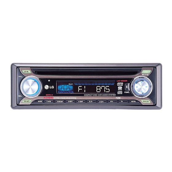
- Page 1 DETACHABLE FRONT PANEL CAR CD RECEIVER SERVICE MANUAL CAUTION BEFORE SERVICING THE UNIT, READ THE “SAFETY PRECAUTIONS” IN THIS MANUAL. MODEL : LAC-M2500R MAY, 2005...
- Page 2 [CONTENTS] SECTION 1. SUMMARY ❍ • SERVICING PRECAUTIONS ......................1-2 • ESD PRECAUTIONS ........................1-3 • SPECIFICATIONS ........................... 1-4 ❍ SECTION 2. ELECTRICAL • ELECTRICAL TROUBLESHOOTING GUIDE ................. 2-1 • WAVEFORMS OF MAJOR CHECK POINT ..................2-6 • INTERNAL BLOCK DIAGRAM of ICs ....................2-7 •...
-
Page 3: Section 1. Summary
SECTION 1. SUMMARY ❏ SERVICING PRECAUTIONS – Always disconnect the power source before: 1) Removing or reinstalling any component, circuit board, module or any other instrument assembly. 2) Disconnecting or reconnecting any instrument electrical plug or other electrical connection. 3) Connecting a test substitute in parallel with an electrolytic capacitor in the instrument. CAUTION: A wrong part substitution or incorrect polarity installation of electrolytic capacitors may result in an explosion hazard. -
Page 4: Esd Precautions
❏ ESD PRECAUTIONS [Electrostatically Sensitive Devices (ESD)] Some semiconductor (solid state) devices can be damaged easily by static electricity. Such omponents commonly are called Electrostatically Sensitive Devices (ESD). Examples of typical ESD devices are integrated circuits and some field-effect transistors and semiconductor chip components. The following techniques should be used to help reduce the incidence of component damage caused by static electricity. -
Page 5: Specifications
❏ SPECIFICATIONS 1. GENERAL Power requirements ........................DC12V~15V Ground system ........................... Negative Dimensions(W x H x D) ...................... 188 x 58 x 166mm Weight .............................. Net: 1.3kg 2. RADIO SECTION AM(MW) Frequency range 65.0~74.0MHz(Optional), 522~1,620kHz 87.5~108MHz (Optional:530~1,710kHz/ 520~1,620kHz) Intermediate frequency 10.8MHz 450kHz Usable sensitivity... -
Page 6: Section 2. Electrical
SECTION 2. ELECTRICAL ❏ ELECTRICAL TROUBLESHOOTING GUIDE (1) NO POWER. Any Key power on. Check power supply circuitry. Q380, Q381, Q382,Q230 Is power turnd on? IC201 Pin1, IC401 Pin3. Check loading supply circuitry. Q350,Q351,Q353, DISC loading? PN505, IC401 Pin1 Check laser circuitry. Does initial reading occur? Q501, IC502 Check focusing circuitry. - Page 7 (2) LCD LIGHT ABNORNAL. Any Key power on. (without DISC) Power supply circuitry defective. Check voltage in the power supply Do display LCD then light? Q371,Q372,IC403 circuitry. Is u-com IC401 reset circuit • Reset circuit defective. normal? Pin88 IC201 Surrounding circuit defective.
- Page 8 (3) INITIAL READING IS NOT CARRIED OUT. Check the Voltage change of Defective connector Slide motor moves CN503 Pin10(6.4~6.8V) CN503 (With disc) Check the Voltage IC501 Pin31 Defective IC501 (1.4V~1.8V) Spindle motor turns Defective connector Check the Data transmission from WAVEFORM #1 CN503 CN503(18,20,21) to CD DSP...
- Page 9 When laser does not light. Is “2.4V~3.4V” applied to pin2 of IC502? ➀ 3.4V ➁ 2.4V) Did pickup return to Is data transferred from Defective MICOM or CN503. innermost circular? MICOM IC ? Does voltage appear at Defective IC501,IC502 IC504 Pin 13, 14? Defective slide motor and/or connector.(CN501) Is defect output from LMT...
- Page 10 When laser light. Laser lights Defective IC501 Check the signal FOCUS SEARCH of IC501 Pin 37 WAVEFORM #3 Defective IC501 Check the signal of IC504 Pin 15, 16 WAVEFORM #3 Degraded laser diode Defective PICK-UP When SPINDLE motor dose not turn Check the change for SPDO Voltage of Defective IC501...
-
Page 11: Waveforms Of Major Check Point
❏ WAVEFORMS OF MAJOR CHECK POINT #1. SPINDLE DRIVE AND MOTOR WAVEFORM #2. RF WAVEFORM IC501(29), IC544(12) when TOC reading IC502(8), IC502(3) during TOC Reading #3. FOCUS DRIVE AND MOTOR WAVEFORM IC501(37), IC504(15) • When focus search failed or there is no disc on tray •... -
Page 12: Internal Block Diagram Of Ics
❏ INTERNAL BLOCK DIAGRAM of ICs I PD784214A(IC401) 1) PORT ASSIGNMENT - 2-7 -... - Page 13 I MN6627933CG(IC501) - 2-8 -...
-
Page 14: Block Diagram
1) BLOCK DIAGRAM - 2-9 -... -
Page 15: Pin Configuration
I AM5810(IC504) 1) BLOCK DIAGRAM 2) PIN CONFIGURATION - 2-10 -... -
Page 16: Pin Descriptions
3) PIN DESCRIPTIONS PIN No Pin Name Description Input for loading forward Input for loading reverse LDCONT Output control terminal for loading Control terminal for power saving mode Input 1 of CH1 Input 2 of CH2 PREVCC Pre and loading unit power supply input terminal POWVCC12 Power unit power supply input terminal (CH1, CH2) VOL ( - ) - Page 17 I AMC1117(IC505) 1) BLOCK DIAGRAM - 2-12 -...
- Page 18 I TDA7348D(IC601) - 2-13 -...
- Page 19 I TA8275H(IC801) - 2-14 -...
- Page 20 I PT6523(IC901) - 2-15 -...
- Page 21 - 2-16 -...
- Page 22 ❏ BLOCK DIAGRAM L-SPEAKER 17,19 2(FL,FR) POWER AMP 11,15 FRONT 25,26 IC803 IC601 TDA7438D R-SPEAKER LINE SW/E.VOLUME 10,14 12,14 TDA8275HQ 23,24 2(RL,FR) L-SPEAKER 21,23 8,12 10,14 REAR TU101 R-SPEAKER 11,12 6,20 9.4V REG CET85XX 2(LR) Q360,ZD361 MUTE 16,17, LINE-OUT CCNTROL 18,19 4,14 (OPTION)
-
Page 23: Main Schematic Diagram
❏ SCHEMATIC DIAGRAM 1. MAIN SCHEMATIC DIAGRAM 2-19 2-20... -
Page 24: Front Schematic Diagram
2. FRONT SCHEMATIC DIAGRAM 2-21 2-22... -
Page 25: Cdp Schematic Diagram
3. CDP SCHEMATIC DIAGRAM 2-23 2-24... -
Page 26: Printed Circuit Diagram
❏ PRINTED CIRCUIT DIAGRAM 1. MAIN P.C. BOARD 2-25 2-26... -
Page 27: Front P.c. Board
2. FRONT P.C. BOARD 2. FRONT P.C. BOARD 2-28 2-29... -
Page 28: Cdp P.c. Board
3. CDP P.C. BOARD 3. CDP P.C. BOARD 2-30 2-31... - Page 29 4. LED P.C.BOARD (TOP) 4. LED P.C.BOARD (BOTTOM) 2-32 2-33...
-
Page 30: Section 3. Cabinet Mainchassis & Mechanism
SECTION 3. CABINET MAINCHASSIS & MECHANISM I EXPLODED VIEW CAUTION Exposed blade will cause severe injury...