Table of Contents
Advertisement
Quick Links
OPERATE
NTSC/PAL
3
SPECIFICATIONS ............................................................................................................................. 1-1-1
LASER BEAM SAFETY PRECAUTIONS .......................................................................................... 1-2-1
IMPORTANT SAFEGUARDS AND PRECAUTIONS ......................................................................... 1-3-1
STANDARD NOTES FOR SERVICING ............................................................................................. 1-4-1
OPERATING CONTROLS AND FUNCTIONS .................................................................................. 1-5-1
CABINET DISASSEMBLY INSTRUCTIONS ..................................................................................... 1-6-1
FIRMWARE RENEWAL MODE ......................................................................................................... 1-7-1
TROUBLESHOOTING ....................................................................................................................... 1-8-1
BLOCK DIAGRAMS ........................................................................................................................... 1-9-1
SCHEMATIC DIAGRAMS/ CBA'S AND TEST POINTS .................................................................. 1-10-1
WAVEFORMS .................................................................................................................................. 1-11-1
WIRING DIAGRAM .......................................................................................................................... 1-12-1
SYSTEM CONTROL TIMING CHARTS .......................................................................................... 1-13-1
IC PIN FUNCTION DESCRIPTIONS ............................................................................................... 1-14-1
LEAD IDENTIFICATIONS ................................................................................................................ 1-15-1
EXPLODED VIEWS ......................................................................................................................... 1-16-1
MECHANICAL PARTS LIST ............................................................................................................ 1-17-1
ELECTRICAL PARTS LIST ............................................................................................................. 1-18-1
SHARP CORPORATION
SERVICE MANUAL
DVD VIDEO PLAYER
MODELS
4
---DV-SL80X
CONTENTS
In the interests of user-safety (Required by safety regula-
tions in some countries) the set should be restored to its
original condition and only parts identical to those specified
be used.
This document has been published to be used for
after sales service only.
The contents are subject to change without notice.
1
DV-SL80/DV-SL80X
S45S9DV-SL80/
DV-SL80
DV-SL80X
Page
Advertisement
Table of Contents

Related Manuals for Sharp DV-SL80


Summary of Contents for Sharp DV-SL80
-
Page 1: Table Of Contents
DV-SL80/DV-SL80X SERVICE MANUAL S45S9DV-SL80/ DVD VIDEO PLAYER OPERATE DV-SL80 NTSC/PAL DV-SL80X MODELS In the interests of user-safety (Required by safety regula- ---DV-SL80 ---DV-SL80X tions in some countries) the set should be restored to its original condition and only parts identical to those specified be used. -
Page 2: Dv-Sl80
NOTES: 1. All Items are measured without pre-emphasis unless otherwise specified. 2. Power supply : AC110 - 240 V ~ 50/60Hz --- [ DV-SL80 ] AC220 - 240 V ~ 50/60Hz --- [ DV-SL80X ] 3. Load imp. : 100 k ohm 4. -
Page 3: Laser Beam Safety Precautions
LASER BEAM SAFETY PRECAUTIONS This DVD player uses a pickup that emits a laser beam. Do not look directly at the laser beam coming from the pickup or allow it to strike against your skin. The laser beam is emitted from the location shown in the figure. When checking the laser diode, be sure to keep your eyes at least 30cm away from the pickup lens when the diode is turned on. -
Page 4: Important Safeguards And Precautions
IMPORTANT SAFEGUARDS AND PRECAUTIONS 1. IMPORTANT SERVICE NOTES BEFORE RETURNING THE DVD VIDEO PLAYER Reverse the AC plug on the set and repeat AC voltage measurements for each exposed part. Any reading of Before returning the DVD video player to the user, 1.4V rms (this corresponds to 0.7mA rms AC.) or more is excessive and indicates a potential shock hazard perform the following safety checks. -
Page 5: Standard Notes For Servicing
STANDARD NOTES FOR SERVICING Circuit Board Indications Using lead-free wire solder a. The output pin of the 3 pin Regulator ICs is indicated When fixing the PWB soldered with the lead-free solder, as shown. apply lead-free wire solder. Repairing with conventional lead wire solder may cause damage or accident due to cracks. - Page 6 Soldering Iron Fig. S-1-3 (2) Lift each lead of the flat pack-IC upward one by one, using a sharp pin or wire to which solder will not adhere (iron wire). When heating the pins, use a fine Fig. S-1-1 tip soldering iron or a hot air desoldering machine.
- Page 7 (4) Bottom of the flat pack-IC is fixed with glue to the 2. Installation CBA; when removing entire flat pack-IC, first apply (1) Using desoldering braid, remove the solder from the soldering iron to center of the flat pack-IC and heat foil of each pin of the flat pack-IC on the CBA so you up.
- Page 8 Instructions for Handling Semi-conductors Electrostatic breakdown of the semi-conductors may occur due to a potential difference caused by electrostatic charge during unpacking or repair work. 1. Ground for Human Body Be sure to wear a grounding band (1MΩ) that is properly grounded to remove any static electricity that may be charged on the body.
-
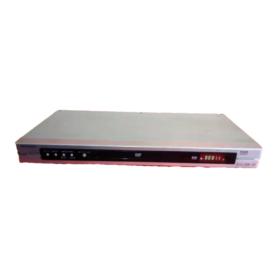
Page 9: Operating Controls And Functions
OPERATING CONTROLS AND FUNCTIONS FRONT PANEL OPERATE REAR VIEW AUDIO OUT COMPONENT VIDEO OUT DIGITAL AUDIO OUT VIDEO S-VIDEO OPTICAL COAXIAL 13 14 1. OPERATE 11. OPTICAL (Digital audio out) to switch the player to ON or OFF connect to digital (optical) audio equipment 2. -
Page 10: Cabinet Disassembly Instructions
Mecha work. [6] AV CBA (S-5), To avoid damage of pickup follow next procedures. 4(S-6)---[DV-SL80] 2-1. Short the three short lands (either of two places) of 5(S-6)---[DV-SL80X], FPC cable with solder before removing the FFC *2(L-5) cable (CN201) from it as shown in “View for A” in... - Page 11 (S-3B) (S-3A) [1] Top Case (S-1) CN201 CN601 CN301 CN401 [4] DVD Main CBA Unit Fig. 1 (L-1) (L-3) Solder Short the three short lands by soldering. Short (Either of two places.) lands (L-1) Short lands (L-2) FPC Cable [2] Front Assembly Fig.
- Page 12 [7] Function CBA [6] AV CBA (S-5) CN2001 DV-DL80X only (S-6) (S-6) (L-5) Fig. 6 HOW TO EJECT MANUALLY (Method 1) 1 Remove the Top Case. 2 Remove the Reinforce Plate. 3 Rotate the roulette in the direction of the arrow as shown below. View for A Rotate this roulette in the direction of the arrow...
- Page 13 HOW TO EJECT MANUALLY (Method 2) 1 Turn the unit over. 2 Insert the shaft less than a diameter of 3 mm (e.g. screwdriver) straightly into the opening as shown. 3 Turn the shaft along with the opening clockwise. 4 Repeat steps 2 and 3 until the tray will open. 5 Pull the tray slowly with a hand.
-
Page 14: Firmware Renewal Mode
FIRMWARE RENEWAL MODE The appearance shown in (*2) of Fig. c is described FIRMWARE is built-in program to operate DVD player. To get rid of error when playing new software (disc) in as follows: the market, FIRMWARE version is updated. Perform Appearance State the following to update the FIRMWARE version. - Page 15 " ******* " differ depending on the models. MODEL : ******* Version : *.** Region : * EEPROM CLEAR : OK EEPROM CLEAR : CLEAR EXIT: POWER Fig. h When "OK" appears on the screen, the factory default will be set. Then the firmware renewal mode is complete.
-
Page 16: Troubleshooting
TROUBLESHOOTING FLOW CHART NO.1 The power cannot be turned on. See FLOW CHART No.2 <The fuse blows out.> Is the fuse normal? Is normal state restored when once unplugged Check if there is any leak or short-circuiting on the power cord is plugged again after several seconds? primary circuit component, and service it if defective. - Page 17 FLOW CHART NO.6 P-ON+10V (EV+11V) is not outputted. Is 11V voltage supplied to the emitter of Q1002? Check D1030, D1048, C1035, C1048, L1009 and the periphery circuit, and service it if defective. Check Q1016 and PWRCON line and service it if Is the voltage of base on Q1002 lower than the defective.
- Page 18 FLOW CHART NO.11 The fluorescent display tube does not light up. Is 3.3V voltage supplied to Pins(6,24) of IC2001? Check the EV+3.3V line and service it if defective. Is the voltage of approximately -20V supplied to Check the -FL (-20V) line and service it if defective. Pin(15) of IC2001? Is there 500kHz oscillation at Pin(26) of IC2001? Check R2002, IC2001 and their periphery, and...
- Page 19 FLOW CHART NO.14 The disc tray cannot be opened and closed. (It can be done using the remote control unit.) Is the normal control voltage inputted to Pin(4) of Replace the "OPEN/CLOSE" button (SW2108). IC2001? Refer to "FLOW CHART NO.12" <The key operation is not functioning.>...
- Page 20 FLOW CHART NO.19 Both functions of picture and sound do not operate normally. Replace the DVD Main CBA. Original DVD Main CBA is poor. No improvement can be found. Replace the DVD Mecha. FLOW CHART NO.20 Picture does not appear normally. Set the disc on the disc tray, and playback.
- Page 21 FLOW CHART NO.21 Audio is not outputted normally. Set the disc on the disc tray, and playback. Replace the DVD Main CBA or DVD Mecha. Are the analog audio signals outputted to each pin of CN1601 on AV CBA? CN1601 14PIN AUDIO-L CN1601 16PIN AUDIO-R Check each line between each pin of CN1601 Are the analog audio signals inputted to each pin...
-
Page 22: Block Diagrams
BLOCK DIAGRAMS System Control / Servo Block Diagram E5943BLS 1-9-1... - Page 23 Digital Signal Process Block Diagram E5943BLD 1-9-2...
- Page 24 Video / Audio Block Diagram E5943BLV 1-9-3...
- Page 25 Power Supply Block Diagram E5943BLP 1-9-4...
-
Page 26: Schematic Diagrams/ Cba's And Test Points
SCHEMATIC DIAGRAMS / CBA’S AND TEST POINTS Standard Notes Notes: 1. Do not use the part number shown on these draw- ings for ordering. The correct part number is shown WARNING in the parts list, and may be slightly different or Many electrical and mechanical parts in this chassis amended since these drawings were prepared. - Page 27 LIST OF CAUTION, NOTES, AND SYMBOLS USED IN THE SCHEMATIC DIAGRAMS ON THE FOLLOWING PAGES: 1. CAUTION: FOR CONTINUED PROTECTION AGAINST FIRE HAZARD, REPLACE ONLY WITH THE SAME TYPE FUSE. 2. CAUTION: Fixed Voltage (or Auto voltage selectable) power supply circuit is used in this unit. If Main Fuse (F1001) is blown, first check to see that all components in the power supply circuit are not defective before you connect the AC plug to the AC power supply.
- Page 28 DVD Main 1/3 Schematic Diagram 1-10-3 1-10-4 E5943SCD1...
- Page 29 DVD Main 2/3 Schematic Diagram 1-10-5 1-10-6 E5943SCD2...
- Page 30 IC101 VOLTAGE CHART PIN.NO PLAY STOP PIN.NO PLAY STOP PIN.NO PLAY STOP PIN.NO PLAY STOP PIN.NO PLAY STOP PIN.NO PLAY STOP PIN.NO PLAY STOP PIN.NO PLAY STOP ----- ----- ----- ----- ----- ----- ----- ----- ----- ----- ----- ----- ----- ----- ----- -----...
- Page 31 DVD Main 3/3 Schematic Diagram Note: IC103 is not supplied separately. Be sure to replace with the DVD Main CBA unit when servicing IC103. 1-10-9 1-10-10 E5943SCD3...
- Page 32 AV 1/3 Schematic Diagram CAUTION ! CAUTION Fixed voltage ( or Auto voltage selectable ) power supply circuit is used in this unit. NOTE : If Main Fuse (F1001) is blown, check to see that all components in the power supply FOR CONTINUED PROTECTION AGAINST FIRE HAZARD, THE VOLTAGE FOR PARTS IN HOT CIRCUIT IS MEASURED USING circuit are not defective before you connect the AC plug to the AC power supply.
- Page 33 AV 2/3 Schematic Diagram 1-10-13 1-10-14 E5943SCAV2...
- Page 34 AV 3/3 & Function Schematic Diagram FL2001 MATRIX CHART SACD SACD PSCAN REPEAT TITLE GROUP PSCAN REPEAT HD VCD GROUP TITLE 1-10-15 1-10-16 E5943SCAV3...
- Page 35 DVD MAIN CBA Top View 1-10-17 1-10-18 BE5900G04012...
- Page 36 DVD MAIN CBA Bottom View 1-10-19 1-10-20 BE5900G04012...
- Page 37 AV CBA Top View CAUTION ! Fixed voltage ( or Auto voltage selectable ) power supply circuit is used in this unit. CAUTION If Main Fuse (F1001) is blown, check to see that all components in the power supply NOTE : FOR CONTINUED PROTECTION AGAINST FIRE HAZARD, circuit are not defective before you connect the AC plug to the AC power supply.
-
Page 38: Av Cba Bottom View
AV CBA Bottom View CAUTION ! Fixed voltage ( or Auto voltage selectable ) power supply circuit is used in this unit. CAUTION If Main Fuse (F1001) is blown, check to see that all components in the power supply NOTE : FOR CONTINUED PROTECTION AGAINST FIRE HAZARD, circuit are not defective before you connect the AC plug to the AC power supply. - Page 39 FUNCTION CBA Top View FUNCTION CBA Bottom View 1-10-25 1-10-26 BE5942F01011B...
-
Page 40: Waveforms
WAVEFORMS Pin 8 of CN1601 Pin 16 of CN1601 VIDEO-Y VIDEO-Y 0.2V 0.2V 20µs AUDIO-R AUDIO-R 0.5ms 0.5ms Pin 10 of CN1601 Pin 19 of CN1601 VIDEO-C VIDEO-C 0.2V 0.2V 20µs SPDIF SPDIF 0.1µs C1402 PLUS LEAD NOTE: Input CD: 1kHz PLAY (WF4~WF6) DVD: POWER ON (STOP) MODE VIDEO-CVBS... -
Page 41: Wiring Diagram
WIRING DIAGRAM 1-12-1 E5943WI... -
Page 42: System Control Timing Charts
SYSTEM CONTROL TIMING CHARTS Tray Close ~ Play / Play ~ Tray Open Tray Disc Disc Tray Play Close Rotation Stop Open 3.3V Tray IN (TL221) Sled Drive 1.65V (TP303) 1.65V Disc Drive (TP301) 1.65V Focus Drive (TP304) Tracking Drive 1.65V (TP302) E5945TI... -
Page 43: Ic Pin Function Descriptions
IC PIN FUNCTION DESCRIPTIONS IC2001 ( PT6313-S -TP ) Signal In/Out Name Function Name FP-CLK Clock Input FP-STB Serial Interface Strobe Key Data 1 Input Key Data 2 Input Power Supply Segment Output / Key a / KEY-1 Souce-1 Segment Output / Key KEY-2 Souce-2 Segment Output / Key... -
Page 44: Lead Identifications
LEAD IDENTIFICATIONS KRA110M KTC3203(Y) 0C-0805T*002 KTA1267(Y) KTA1266 (Y) KTC3199(GR,Y) 1 2 3 E C B E C B PQ070XZ5MZP PT6313-S-TP KIA431-AT KIA4558P 1: Vin 2: Vc 3: Vo 4: Vadj 5: GND 1 2 3 K A R MM1637XVBE 2SK3566 LTV-817B-F Note: A: Anode... -
Page 45: Exploded Views
2L081 2L011 2L081 2L021 2L021 2L021 Comparison Chart of Models and Marks 2L105 DVD Main Model Mark CBA Unit DV-SL80 2L105 DV-SL80X 2L021 JK1401 JK1404 JK1202 [ B ] IC1204 2L031 Function CBA F1001 AV CBA [ A ] AC1001... - Page 46 Packing Unit E5943EX 1-16-2...
-
Page 47: Mechanical Parts List
PRODUCT SAFETY NOTE: Products marked with a ! have special characteristics important to safety. Before replacing any of these components, read carefully the product safety notice in this service manual. Don't degrade the safety of the product through improper servicing. COMPARISON OF MODELS Model Mark DV-SL80 DV-SL80X Ref. No. Mark Description Part No. -
Page 48: Electrical Parts List
C..±0.25% D..±0.5% F..±1% G..±2% J..±5% K..±10% M..±20% N..±30% Z..+80/-20% COMPARISON OF MODELS Model Mark DV-SL80 DV-SL80X DVD MAIN CBA UNIT Ref. No. Mark Description Part No. Code DVD MAIN CBA UNIT 9HSN79S2HHP DVD MAIN CBA UNIT 9HSN79S4HAP Consists of the following... - Page 49 Ref. No. Mark Description Part No. Code C191 CHIP CERAMIC CAP.(1005) CH J 15pF/50V 9HSHB1JJ3CH150 C192 CHIP CERAMIC CAP.(1005) CH J 22pF/50V 9HSHB1JJ3CH220 C195 CHIP CERAMIC CAP.(1005) F Z 0.1µF/16V 9HSHB1CZ30F104 C196 CHIP CERAMIC CAP.(1005) F Z 0.1µF/16V 9HSHB1CZ30F104 C201 CHIP CERAMIC CAP.(1005) F Z 0.1µF/16V 9HSHB1CZ30F104 C202...
- Page 50 Ref. No. Mark Description Part No. Code C412 CHIP CERAMIC CAP.(1005) F Z 0.1µF/16V 9HSHB1CZ30F104 C416 CHIP CERAMIC CAP.(1005) F Z 0.1µF/16V 9HSHB1CZ30F104 C417 CHIP CERAMIC CAP.(1005) F Z 0.1µF/16V 9HSHB1CZ30F104 C418 CHIP CERAMIC CAP.(1005) F Z 0.1µF/16V 9HSHB1CZ30F104 C421 CHIP CERAMIC CAP.(1005) CH J 47pF/50V 9HSHB1JJ3CH470 C422...
- Page 51 Ref. No. Mark Description Part No. Code COILS L104 CHIP BEAD MMZ1608Y121CT 9HSL06001TE004 CHIP RES.(1608) 1/10W 0 Ω L106 9HSRXAJR5Z0000 CHIP RES.(1608) 1/10W 0 Ω L107 9HSRXAJR5Z0000 L108 CHIP INDUCTOR LB2016T2R2M 9HSLC2R2MTU007 L201 CHIP INDUCTOR LB2012T470M 9HSLC470MTU038 CHIP RES.(1608) 1/10W 0 Ω L250 9HSRXAJR5Z0000 L401...
- Page 52 Ref. No. Mark Description Part No. Code CHIP RES.(1005) 1/16W J 470 Ω R265 9HSRXGJR4Z0471 CHIP RES.(1005) 1/16W J 180 Ω R268 9HSRXGJR4Z0181 CHIP RES.(1005) 1/16W J 8.2k Ω R270 9HSRXGJR4Z0822 CHIP RES.(1005) 1/16W J 18k Ω R271 9HSRXGJR4Z0183 CHIP RES.(1005) 1/16W J 4.7k Ω R274 9HSRXGJR4Z0472 CHIP RES.(1005) 1/16W J 6.8k Ω...
- Page 53 AV CBA + FUNCTION CBA Ref. No. Mark Description Part No. Code AV CBA + FUNCTION CBA 9HS1VSA10081 Consists of the following AV CBA 9HS1VSA10081A FUNCTION CBA 9HS1VSA10081B AV CBA + FUNCTION CBA 9HS1VSA10069 Consists of the following AV CBA 9HS1VSA10069A FUNCTION CBA 9HS1VSA10069B...
- Page 54 Ref. No. Mark Description Part No. Code C1361 ELECTROLYTIC CAP. 220µF/6.3V M H7 9HSE0KMASSL221 C1362 CHIP CERAMIC CAP.(1608) F Z 0.1µF/50V 9HSHD1JZ30F104 C1394 ELECTROLYTIC CAP. 47µF/10V M 9HSE1AMASDL470 C1395 ELECTROLYTIC CAP. 1000µF/6.3V M 9HSE0KMASDL102 C1402 ELECTROLYTIC CAP. 470µF/6.3V M 9HSE0KMASDL471 C1421 CHIP CERAMIC CAP.(1608) B K 0.01µF/50V 9HSHD1JK30B103...
- Page 55 Ref. No. Mark Description Part No. Code IC2001 FL DRIVER IC PT6313-S-TP 9HSSZBA0TG2006 COILS L1001! LINE FILTER 50MH LF-4Z-E503 9HSLBG00ZKQ008 L1007 CHOKE COIL 22µH-K 9HSLBD00PKV006 L1008 PCB JUMPER D0.6-P5.0 9HSJW5.0T L1009 CHOKE COIL 22µH-K 9HSLBD00PKV006 L1060 PCB JUMPER D0.6-P5.0 9HSJW5.0T L1350 INDUCTOR(100µH K) LAP02TA101K 9HSLAXKATTU101...
- Page 56 Ref. No. Mark Description Part No. Code CARBON RES. 1/6W J 820 Ω R1068 9HSCX6JATZ0821 CARBON RES. 1/4W J 560 Ω R1069 9HSCX4JATZ0561 CHIP RES.(1608) 1/10W J 680 Ω R1072 9HSRXAJR5Z0681 METAL OXIDE FILM RES. 2W J 33 Ω R1073 9HSN02330ZU001 R1074 RECTIFIER DIODE 1N4005...
- Page 57 Ref. No. Mark Description Part No. Code CHIP RES.(1608) 1/10W J 6.8k Ω R2031 9HSRXAJR5Z0682 CHIP RES.(1608) 1/10W J 10k Ω R2032 9HSRXAJR5Z0103 CHIP RES.(1608) 1/10W J 22k Ω R2033 9HSRXAJR5Z0223 CHIP RES.(1608) 1/10W J 10k Ω R2041 9HSRXAJR5Z0103 CHIP RES.(1608) 1/10W J 10k Ω R2042 9HSRXAJR5Z0103 CHIP RES.(1608) 1/10W J 10k Ω...
- Page 58 DV-SL80/DV-SL80X © COPYRIGHT 2004 BY SHARP CORPORATION ALL RIGHTS RESERVED. No part of this publication may be reproduced, stored in a retrieval system, or transmitted in any form or by any means, electronic, mechanical, photocopying, recording, or otherwise, without prior written permission of the publisher.