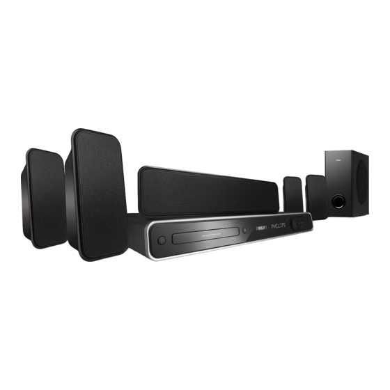
Philips HTS3365/55 Service Manual
Hide thumbs
Also See for HTS3365/55:
- Quick start manual (2 pages) ,
- Manual (57 pages) ,
- Service manual (35 pages)
Advertisement
Quick Links
Download this manual
See also:
Manual
DVD Home Theater System
Service
Service Manual
©
Copyright 2008 Philips Consumer Electronics B.V. Eindhoven, The Netherlands
All rights reserved. No part of this publication may be reproduced, stored in a retrieval system or
transmitted, in any form or by any means, electronic, mechanical, photocopying, or otherwise
without the prior permission of Philips.
Published by
LM0811
Service Audio Printed in The Netherlands Subject to modification
Version 1.0
TABLE OF CONTENTS
Location of PCB Boards .............................................. 1-2
Versions Variation ....................................................... 1-2
Specifications .............................................................. 1-3
Measurement setups ................................................... 1-4
Service Aids................................................................. 1-5
ESD & Safety instruction ............................................. 1-6
Lead-tree solding information ...................................... 1-7
Setting procedure & Repair instructions ......................... 2
Disassembly instruction & Service Postion .................... 3
Block & Wring Diagram .................................................. 4
VFD+JACK+VOL+STANDBY Board .............................. 5
Main Board ..................................................................... 6
Power Board................................................................... 7
AMP Board ..................................................................... 8
Mechanical Exploded View & Parts................................ 9
Revision List ................................................................. 10
1 - 1
Chapter
HTS3365/
55
GB
3139 785 33640
Advertisement

Related Manuals for Philips HTS3365/55


Summary of Contents for Philips HTS3365/55
- Page 1 Revision List ..............10 © Copyright 2008 Philips Consumer Electronics B.V. Eindhoven, The Netherlands All rights reserved. No part of this publication may be reproduced, stored in a retrieval system or transmitted, in any form or by any means, electronic, mechanical, photocopying, or otherwise without the prior permission of Philips.
- Page 2 1 - 2 LOCATION OF PCB BOARDS MAIN PCB AMP PCB STANDBY PCB VFD PCB Power PCB VOL PCB JACK PCB VERSION VARIATION: HTS3365 Type/Versions Features Main(Power Output-600W) S-video out Power Voltage (120V/230V) SERVICE SCNARIO MATRIX: HTS3365 Type/Versions Boards in used Main Board Power Board AMP Board...
- Page 3 1 - 3 SPECIFICATIONS MAIN UNIT AMPLIFIER Power Supply Rating ..110-127 V / 220-240 V~; Total output power ..............50-60 Hz Home Theatre mode ........600 W Power Consumption ........100 W Frequency Response ..180 Hz – 18 kHz / ±3 dB Dimensions ......
- Page 4 1 - 4 MEASUREMENT SETUP Tuner FM Bandpass Tuner AM (MW,LW) Bandpass...
- Page 5 1 - 5...
- Page 6 1 - 6...
- Page 7 1 - 7...
- Page 8 “ok” button to con rm * the system will switch off and on again automatically. c) TV will show message as below: e) OSD will show: Current model HTS3365/55 Version: 00.12.01_1 Release: 2007.12.19 upgrade le detected region Servo: 5B.61.00.00 Do you wish to continue with 8032: 05.00.04.06...
- Page 9 2 - 2 2 - 2 REPAIR INSTRUCTIONS (part one)
- Page 10 2 - 3 2 - 3 REPAIR INSTRUCTIONS (part two)
- Page 11 2 - 4 2 - 4 REPAIR INSTRUCTIONS (part three)
- Page 12 3 - 1 3 - 1 DISASSEMBLY INSTRUCTIONS Dismantling of the Front Panel Assemble 3) Loosen 7 screws and remove the Top Cover by lifting the rear portion upwards before sliding it out towards the rear. - 1 screw “A” each on the left & right side as shown in gure 4 1) Open the DVD Tray by using the Open/Close Button while the Set is ON and disconnect the mains supply after removing the Tray - 5 screws “B”...
- Page 13 3 - 2 3 - 2 Dismantling of the Main Board Dismantling of the VFD+JACK+VOL+STANDBY Board 1) Loosen 2 screws “ G “ on the top of main board as shown in gure10 1) Loosen 9 screws “J” on the top of control board as shown in 13 2) Loosen 7 screws “H”...
- Page 14 4 - 1 4 - 1 BLOCK DIAGRAM...
- Page 15 4 - 2 4 - 2 WIRING DIAGRAM...
- Page 16 5 - 1 5 - 1 FTD DISPLAY PIN ASSIGNMENT CONTROL BOARD TABLE OF CONTENTS FTD Display Pin Assignment ............. 5-1 Circuit Diagram ................. 5-2 PCB Layout Top & Bottom View ............5-3 PIN CONNECTION...
- Page 17 5 - 2 5 - 2 CIRCUIT DIAGRAM FB11 FB17 RB14 SN11 TA18 CN12 FB12 IC11 RB15 TA11 TA19 FB13 JK11 RB16 TA12 TA20 FB14 JK12 RB11 RB17 TA13 USB11 D3 FB15 LD11 RB12 RB18 TA14 VR11 DP11 FB16 RB13 RB19 TA15...
- Page 18 5 - 3 5 - 3 PCB LAYOUT - TOP VIEW CN12 A2 JK11 A4 RB14 A1 RB18 A4 TA12 A1 TA18 A4 VR11 A3 JK12 A4 RB11 A1 RB15 A4 RB19 A4 TA13 A4 TA19 A4 LD11 A1 RB12 A1 RB16 A4 SN11 A1 TA14 A1...
- Page 19 6 - 1 6 - 1 INTERNAL IC DIAGRAM - AS81F641642C MAIN BOARD TABLE OF CONTENTS Internal IC Diagram ................6-1 Circuit Diagram (part one) ..............6-2 INTERNAL IC DIAGRAM - MT1389E Circuit Diagram (part two) ..............6-3 PCB Layout Top View ..............6-4 PCB Layout Bottom View ..............
- Page 20 6 - 2 6 - 2 CIRCUIT DIAGRAM - part one C301 CE307 R302 C302 CE308 R3020 C305 CE309 R305 C306 CE310 R306 C309 CE311 R307 C311 CE312 R308 C313 CE313 R309 C315 CE314 R310 C316 CE315 R313 C317 CE316 R314 C318 CE317...
- Page 21 6 - 3 6 - 3 CIRCUIT DIAGRAM - part two C0201 C2 C242 CE203 D2 IC202 C5 R237 C0202 A3 C243 CE204 D2 IC203 D3 R238 C0203 A3 C253 CE205 D2 IC204 D3 R239 C0204 D1 C254 CE206 D2 IC205 D4 R242 C0205 A3...
- Page 22 6 - 4 6 - 4 PCB LAYOUT - TOP VIEW C0202 A3 C365 B5 CN201 B3 IC801 C5 R249 C3 R384 B5 C0207 C2 C601 A2 CN202 C3 JK302 A4 R250 B1 R418 A5 C0208 C3 C602 A2 CN203 B3 JK601 A3 R251 C3 R419 A5...
- Page 23 6 - 5 6 - 5 PCB LAYOUT - BOTTOM VIEW C0201 B4 C324 B2 CE312 B1 L301 C0203 B4 C518 C1 CE313 B1 Q601 A3 C0204 B4 C519 C1 CE314 A1 Q705 A3 C0205 C5 C520 C1 CE315 A1 Q706 A3 C0206 B5 C521 C1...
-
Page 24: Internal Ic Diagram
7 - 1 7 - 1 INTERNAL IC DIAGRAM - AP3843GMTR UVLO 2.50V INTERNAL BIAS VREF GOOD OUTPUT LOGIC POWER BOARD OVER TEMP PROTECT ERROR COMP LATCH CURRENT SENSE COMPARATOR TABLE OF CONTENTS Internal IC Diagram ................7-1 Circuit Diagram .................. 7-2 PCB Layout Top View ............... - Page 25 7 - 2 7 - 2 CIRCUIT DIAGRAM BD901 A1 C917 C931 C946 C959 C970 CN907 B4 D916 GT901 B1 L906 Q916 R910 R926B A4 R941 R958 R973 R989 TVR901 A1 ZD912 A3 C901 C919 C932 C948 C960 C971 CN908 B4 D917 GT903 B1 L907...
- Page 26 7 - 3 7 - 3 PCB LAYOUT - TOP VIEW BD901 A1 C921 C945 C960 C971 CN907 B4 D920 GT901 B1 J910 J918 J927 L901 Q901 Q915 R917 R943 R966 T901 ZD908 C901 C922 C946 C961 C977 CN908 C4 D921 GT903 C2 J911...
- Page 27 7 - 4 7 - 4 PCB LAYOUT - BOTTOM VIEW C906 A1 C923 A3 C917 B1 D909 B1 R919 B1 R926C B1 ZD902 B1 C927 B2 R973 B2 C955 C1 R955 C1 R989A C1 C926 C2 C978 C2 R981 C2 C941 C3 D915 C3 R959 C3...
- Page 28 8 - 1 8 - 1 INTERNAL IC DIAGRAM - STA309A OUT1A/B LRCKI OUT2A/B BICKI SERIAL OVERSAMPING OUT3A/B SDI12 DATA OUT4A/B SDI34 SYSTEM OUT5A/B CONTROL SDI56 OUT6A/B SKI78 OUT7A/B AMP BOARD OUT8A/B VARIABLE TREBLE VOLUME CHANNEL OVER- BASS EQ LRCKO LIMITING MAPPING SAMPLING...
-
Page 29: Circuit Diagram
8 - 2 8 - 2 CIRCUIT DIAGRAM C412 C440 C455 C477 C503 C521 C538 CE406 B3 D404 FB405 A1 L409 Q416 R407 R430 R455 R484 R514 R529 RB601 D3 C413 C441 C461 D4 C478 C504 C522 C539 CE407 B3 D405 FB406 A1 L410... -
Page 30: Pcb Layout Top View
8 - 3 8 - 3 PCB LAYOUT - TOP VIEW C545 R455 C425 C601 R456 C425A D4 C602 R458 C426 CN401 D1 R462 C427 CN402 A1 R473 C427A C3 CN403 C1 R474 C428 D406 R482 C443 D407 R483 C448 D420 R484 C449... -
Page 31: Pcb Layout Bottom View
8 - 4 8 - 4 PCB LAYOUT - BOTTOM VIEW D405 B4 R531 A3 C401 D2 D408 B4 R533 A3 C402 D2 D410 A3 C403 D1 D411 A3 C404 D1 D412 A2 C405 C2 D413 A3 C406 C2 D414 A2 C407 C2 D415 A2 C408 C2... - Page 32 9 - 1 9 - 1 MECHANICAL EXPLODED VIEW A1=14+15+37+39...
- Page 33 9 - 2 9 - 2 MECHANICAL PART LIST C920 996510012510 COND SAFETY 0.001uF 400V T901 996510012522 SWTRANS EC-39DWKB486-8519 600W Loc. 12NC. Description C921 994000005343 COND SAFETY 0.22UF 275V 20% T901 996510012523 SW TRANS ER39/40 600W 8+8PIN C922 996500027115 CAP.SAFTY Y1 102PF 250V 20% Y5 T902 994000001057 SW.
- Page 34 9 - 3 9 - 3 Q804 996500026927 XISTR PNP 2SB1132RT100 ROHM HF Q805 996510004117 FET 2SK3018 30V/0.1A SC-70 Q901 996510000615 XISTR NPN 2SC945P Q903 996500026946 XISTR PNP 2SB772P/Q NEC PB<10 Q904 994000005335 XISTR NPN TIP41C ZD901 994000005204 DIODE ZENR 12.6-13.1V 0.5W ZD903 996510010364 DIODE ZENER 5.32-5.88V 0.5W...
- Page 35 10 - 1 10 - 1 REVISION LIST Version 1.0 *Initial release...