Table of Contents
Advertisement
Quick Links
See also:
Handbook
SERVICE MANUAL
Ver. 1.1 2008.05
Revision History
Revision History
Internal memory
Internal memory
ON BOARD
ON BOARD
Link
Link
SPECIFICATIONS
SERVICE NOTE
DISASSEMBLY
• Precaution on Replacing the SY-210 Board
The components identified by
mark 0 or dotted line with
mark 0 are critical for safety.
Replace only with part num-
ber specified.
DSC-H10_L2
9-852-268-31
BLOCK DIAGRAMS
FRAME SCHEMATIC DIAGRAM
SCHEMATIC DIAGRAMS
Les composants identifiés par une
marque 0 sont critiques pour la
sécurité.
Ne les remplacer que par une pièce
portant le numéro spécifié.
Sony EMCS Co.
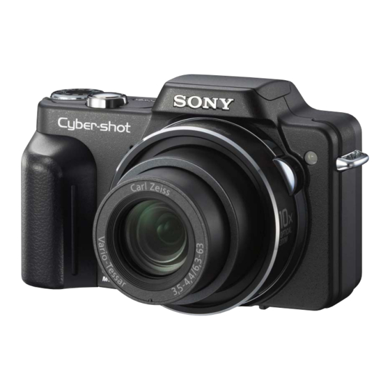
DSC-H10
Photo: Black
DIGITAL STILL CAMERA
LEVEL
US Model
Canadian Model
AEP Model
UK Model
E Model
Australian Model
Hong Kong Model
Chinese Model
Korea Model
Argentine Model
Brazilian Model
Thai Model
Japanese Model
Tourist Model
PRINTED WIRING BOARDS
REPAIR PARTS LIST
Published by Kohda TEC
2
2008E0800-1
© 2008.05
Advertisement
Table of Contents

Related Manuals for Sony DSC-H10


Summary of Contents for Sony DSC-H10
- Page 1 0 are critical for safety. sécurité. Replace only with part num- Ne les remplacer que par une pièce ber specified. portant le numéro spécifié. DIGITAL STILL CAMERA 2008E0800-1 DSC-H10_L2 © 2008.05 Sony EMCS Co. 9-852-268-31 Published by Kohda TEC...
-
Page 2: Specifications
SPECIFICATIONS Camera [Input and Output connectors] BC-CSG/BC-CSGB/BC-CSGC battery charger Multi connector: Video output [System] Audio output (Monaural) Power requirements: AC 100 V to 240 V, 50/ Image device: 7.18 mm (1/2.5 type) color CCD, USB communication 60 Hz, 2.6 W (BC-CSGB)/ Primary color filter USB communication: Hi-Speed USB (USB 2.0 2 W (BC-CSGC) -
Page 3: Safety Check-Out
CRITIQUES POUR LA SÉCURITÉ DE FONCTIONNEMENT. NE COMPONENTS WITH SONY PARTS WHOSE PART NUMBERS REMPLACER CES COMPOSANTS QUE PAR DES PIÈSES SONY APPEAR AS SHOWN IN THIS MANUAL OR IN SUPPLEMENTS DONT LES NUMÉROS SONT DONNÉS DANS CE MANUEL OU PUBLISHED BY SONY. -
Page 4: Self-Diagnosis Function
ENGLISH JAPANESE ENGLISH JAPANESE 1. SERVICE NOTE 1-1. PRECAUTION ON REPLACING THE SY-210 BOARD DESTINATION DATA When you replace to the repairing board, the written destination data of repairing board also might be changed to original setting. Refer to Service Manual ADJ, and perform “DESTINATION DATA WRITE”. USB SERIAL No. -
Page 5: Self-Diagnosis Code Table
ENGLISH JAPANESE ENGLISH JAPANESE 1-2-3. Self-diagnosis Code Table Self-diagnosis Code Block Detailed Symptom/State Correction Function Code The internal memory has experienced a Format the internal memory. format error. “Memory Stick Duo” is unformatted. Format the “Memory Stick Duo”. “Memory Stick Duo” is broken. Insert a new “Memory Stick Duo”. -
Page 6: Process After Fixing Flash Error
ENGLISH JAPANESE ENGLISH JAPANESE 1-3. PROCESS AFTER FIXING FLASH ERROR When “FLASH error” (Self-diagnosis Code E : 91 : 01) occurs, to prevent any abnormal situation caused by high voltage, setting of the flash is changed automatically to disabling charge and flash setting. After fixing, this setting needs to be deactivated. -
Page 7: How To Write Data To Internal Memory
To change the setting, use the write enable tool “WriteEnableTool.exe”. Data writing method Connect the PC to the camera (USB mode: Mass Storage), and switch the driver to the “Sony Seus USB Driver”. Start the Write Enable Tool and the SeusEX. -
Page 8: Service Note
ENGLISH JAPANESE ENGLISH JAPANESE 1. SERVICE NOTE 1-1. SY-210基板交換時の注意 仕向けデータ 補修用基板と交換する時,補修用基板に書かれている仕向けデータは元の設定と違っている場合があります。 ADJ編を参照して,「DESTINATION DATA WRITE」を行ってください。 USBシリアルNo. セットは,1台毎に異なる固有のID(USB Serial No.)を書き込んだ後,出荷されています。 新品の補修用基板には,このIDが書き込まれていないので,基板交換後にIDを入力する必要があります。 ADJ編を参照して,「USB SERIAL No. INPUT」を行ってください。 1-2. 自己診断機能 1-2-2. 自己診断表示 1-2-1. 自己診断機能について 本機の動作に不具合が生じたとき,LCD画面にアルファベッ 本機の動作に不具合が生じたとき,自己診断機能が働き, トと4桁の数字が表示され,3.2Hzで点滅します。この5文字 L C D 画面に,どう処置したらよいか判断できる表示を行い の表示によって対応者分類および不具合の生じたブロックの ます。自己診断機能については取扱説明書にも掲載されて 分類,不具合の詳細コードを示します。 います。 LCD画面... - Page 9 ENGLISH JAPANESE ENGLISH JAPANESE 1-2-3. 自己診断コード表 自己診断コード ブロック 詳細 症状/状態 対応/方法 機能 コード 内蔵メモリにフォーマットエラーが 内蔵メモリをフォーマットする。 あった。 “メモリースティック デュオ”をフォーマットする。 フォーマットしていない“メモリー スティック デュオ”を入れた。 新しい“メモリースティック デュオ”に交換する。 “メモリースティック デュオ”が 壊れている。 “メモリースティック デュオ”の 規格内の“メモリースティック デュオ”を挿入する。 タイプエラーを検出した。 電源の入れ直し,または“メモリースティック デュオ” “メモリースティック デュオ”が 読み/書きできない。 の挿し/外しを数回試す。 ハードウェアトラブルを検出した。 電源を入れ直す。 フォーカスが合いにくい。 操作スイッチの電源を入れ直す。...
- Page 10 ENGLISH JAPANESE ENGLISH JAPANESE 1-3. フラッシュエラー発生時の対処法 本機はフラッシュエラー(自己診断コードE:91:01)が発生した場合,高電圧による異常を防止するために自動的にフラッシュ 充電および発光禁止の設定になります。 フラッシュエラー発生後はエラーの解除を行う必要があります。エラーの解除はホーム画面から初期化操作を実行することによ り行います。 設定リセット お買い上げ時の設定に戻します。 [設定リセット] を実行しても、 内蔵メモリーに記録されている画像は削除されません。 / / / コントロールボタンの で [設定リセット] を選び、 中央の を押す。 「全ての設定内容をリセットします」 というメッセージが表示される。 で [実行] を選び、 中央の を押す。 設定リセットが実行される。 設定リセットを中止するには 手順 で、 [キャンセル] を選び、 中央の を押す。 設定リセット中は電源が切れないようにご注意ください。 1-4.
- Page 11 ENGLISH JAPANESE ENGLISH JAPANESE 1-5. 内蔵メモリへデータを書き戻す方法 通常は,PCからカメラの内蔵メモリへデータを書き込むことはできない設定になっています。 基板交換後などに,内蔵メモリへデータを書き戻す場合には,この設定を一時的に変更する必要があります。 設定の変更には,書き込み許可ツール(WriteEnableTool.exe)を使用します。 書き戻し方法 カメラとPCをマスストレージ接続し,ドライバを“Sony Seus USB Driver”に切り替える。 書き込み許可ツールとSeusEXを起動する。 書き込み許可ツールの[Activate Write Enable Mode]ボタンをクリックする。 設定の変更が終了すると,次のメッセージが表示されます。 ドライバを元に戻して、カメラとPCをマスストレージ接続する。 PCに読み出しておいたデータをカメラの内蔵メモリに書き込む。 カメラとPCの接続を解除し,カメラの電源をOFFにする。 注意: カメラの電源をOFFにすることにより,書き込み許可の設定が解除されます。 DSC-H10_L2 1-8E...
-
Page 12: Note For Repair
2. DISASSEMBLY NOTE FOR REPAIR • Make sure that the flat cable and flexible board are not cracked of bent at the terminal. Cut and remove the part of gilt Do not insert the cable insufficiently nor crookedly. which comes off at the point. (Be careful or some •... -
Page 13: Identifying Parts
2-1. IDENTIFYING PARTS Cabinet (Upper) ⋅ ST-193 Flexible Board ⋅ FL-179 Flexible Board ⋅ PL-048 Flexible Board Cabinet (Rear) SW-530 Board PD-360 Flexible Board BT Holder Section ⋅ MS-403 Board ⋅ JK-373 Flexible Board SY-210 Board Cabinet (Front) LCD Module Lens Block ⋅... -
Page 14: Exploded View
HELP HELP 2-2. DISASSEMBLY EXPLODED VIEW HARDWARE LIST 2-2-1. CABINET (FRONT) SECTION Follow the disassembly in the numerical order given. 1 Side Cover (Lower) (1-1 to 1-3) 2 Cabinet (Front) (2-1 to 2-9) Note: High-voltage cautions Discharging the Capacitor Short-circuit between the two points with the short jig about 10 seconds. -
Page 15: Cabinet (Rear)
2-2-2. CABINET (REAR) SECTION EXPLODED VIEW HARDWARE LIST Follow the disassembly in the numerical order given. 1 Cabinet (Rear) (1-1 to 1-4) 2 Cabinet (Upper) (2-1 to 2-8) 1 Cabinet (Rear) 2 Cabinet (Upper) 1-4 (MC Connector) (Claw) 1-2 (#23) 1-3 (Claw) (Claw) HELP01... - Page 16 2-2-3. CABINET (UPPER) SECTION EXPLODED VIEW HARDWARE LIST Follow the disassembly in the numerical order given. 1 FL-179 Flexible Board (1-1 to 1-14) 2 ST-193 Flexible Board (2-1 to 2-7) 3 PL-048 Board (3-1 to 3-4) When install the ST case (Upper) assy, attach claws A and B in alphabetical order.
-
Page 17: Lcd Block
2-2-4. MAIN BOARD SECTION EXPLODED VIEW HARDWARE LIST Follow the disassembly in the numerical order given. 1 LCD Block (1-1 to 1-2) 2 Lens Block (2-1 to 2-4) 3 SY-210 Board (3-1 to 3-5) 1 LCD Block In case of attaching SY radiation sheet, be sure to attach it in the center of IC softly. - Page 18 2-2-5. BT HOLDER SECTION EXPLODED VIEW HARDWARE LIST Follow the disassembly in the numerical order given. 1 MS-403 Board (1-1 to 1-4) 2 SW-530 Board (2-1 to 2-8) 3 JK-373 Flexible Board (3-1 to 3-4) 4 BT Holder (4-1 to 4-2) 2 SW-530 Board 2-2 (#23) (Boss)
- Page 19 HELP Sheet attachment positions and procedures of processing the flexible boards/harnesses are shown. HELP01 HELP02 To cover the connector of the ST-193 flexible board and the FL-179 flexible board, the insulating sheet (lower) is put. Insulating sheet (lower) Hook Hook FL-179 flexible board Connector of the Speaker Harness...
- Page 20 HELP04 THE METHOD OF ATTACHMENT OF FL-179 FLEXIBLE BOARD 3 Connect the FL-179 flexible board to the 1 Fold dotted line parts of the FL-179 flexible board, PL-048 flexible board. and attach the FL insulating sheet as shown in figure. FL-179 Flexible Board...
- Page 21 7 Open the ST assy, and install the ST case 5 Open the ST assy, and install the ST base (lower) assy as shown in figure. as shown in figure. Claws ST Base ST case (lower) assy Open the ST Assy Bosses Open the ST Assy...
- Page 22 9 Set the flash part of the FL-179 flexible board as shown in figure. FL-179 Flexible Board Valley fold Smooth out the slack of flexible cable. Install ST Case (Upper) Assy by attaching claws A and B in alphabetical order and secure it with a screw. ST Case (Upper) Assy Claw B Claw A...
- Page 23 HELP05 THE METHOD OF ATTACHMENT OF PL-048 FLEXIBLE BOARD 4 Install the PL-048 flexible board, AF holder 1 Attach the AF spacer as shown in figure. in the ST assy as shown in figure. It should not be out of the flexible Push it to cable form.
- Page 24 HELP06 Aligne the switch part of the cabinet (upper) assy with the switch part of the ST-193 flexible board. Cabinet (Upper) Assy Switch Part ST-193 Flexible Board Switch Part HELP07 BT Holder Sheet KK Main Frame LCD Flexible Cable (Be careful about the both sides of the flexible cable don't go out of the sheet.)
- Page 25 HELP08 Lens flexible cable Lens Block Assy Lens Flexible is soldered. Protection Sheet Lens Block Assy From the lens engaged line, upward within 1mm and Lens Retainer Cushion downward within 0mm. Lens Block Assy CD Radiation Sheet 0 ± 0.5mm 1 ±...
-
Page 26: Main Frame
HELP09 Attach BT Terminal Insulating Sheet along the SW-530 board avoiding the main frame. Main Frame BT Terminal Insulating Sheet SW-530 Board HELP10 It does't have to go out of the outline of flexible board. 1 ± 0.5mm Sheet (JK) JK-373 Flexible Board DSC-H10_L2 HELP... - Page 27 HELP11 INSTALLATION METHOD OF BATTERY TERMINAL BOARD 1 Insert the battery terminal board into a slit in the BT holder to install. * The battery terminal board is attached with the notch for installation. BT holder Notch Battery terminal Battery terminal board board 2 Fold the notch 3 or 4 times repeatedly to break.
-
Page 28: Overall Block Diagram
3. BLOCK DIAGRAMS Link Link OVERALL BLOCK DIAGRAM (1/2) POWER BLOCK DIAGRAM (1/2) OVERALL BLOCK DIAGRAM (2/2) POWER BLOCK DIAGRAM (2/2) DSC-H10_L2... - Page 29 3. BLOCK DIAGRAMS 3-1. OVERALL BLOCK DIAGRAM (1/2) ( ) : Number in parenthesis ( ) indicates the division number of schematic diagram where the component is located. PD-360 FLEXIBLE CD-708 FLEXIBLE BOARD SY-210 BOARD (1/2) LENS BLOCK BOARD LCD901 IRIS LENS CN704...
- Page 30 3-2. OVERALL BLOCK DIAGRAM (2/2) ( ) : Number in parenthesis ( ) indicates the division number of schematic diagram where the component is located. JK-373 FLEXIBLE SY-210 BOARD (2/2) BOARD (2/2) CN702 (2/2) XPWR_ON XPOWER_ON ST-193 FLEXIBLE BOARD CN701 S103 XPWR_ON XPWR_ON...
- Page 31 3-3. POWER BLOCK DIAGRAM (1/2) ( ) : Number in parenthesis ( ) indicates the division number of schematic diagram where the component is located. JK-373 FLEXIBLE SY-210 BOARD (1/2) VL_3V BOARD F001 CN702 L001 F002 ACV_UNREG2 ACV_UNREG Q001, 002 IC001 FB701 DC/DC CONVERTER,...
- Page 32 3-4. POWER BLOCK DIAGRAM (2/2) ( ) : Number in parenthesis ( ) indicates the division number of schematic diagram where the component is located. PD-360 FLEXIBLE BOARD SY-210 BOARD (2/2) CHARGE IC701 IC502 PUMP 6.4V REG LCD901 2.8V REG (10/10) CN704 CN001...
- Page 33 4. PRINTED WIRING BOARDS AND SCHEMATIC DIAGRAMS 4-1. FRAME SCHEMATIC DIAGRAM BT901 BATTERY TERMINAL PL-048 FLEXIBLE BOARD D003 BOARD SELF-TIMER/ AF ILLUMINATOR (FLASH UNIT) CN001 FL-179 FLEXIBLE BOARD CN201 (MULTI CONNECTOR) S102 (PLAY) JK-373 FLEXIBLE BOARD J201 DC IN MS-403 BOARD S101 STROBE POP-UP DETECT...
-
Page 34: Schematic Diagrams
4-2. SCHEMATIC DIAGRAMS Link Link PD-360 FLEXIBLE BOARD JK-373 FLEXIBLE BOARD (SY-SW CONNECTION, LCD CONNECTION) (BATTERY IN/DC IN) ST-193 FLEXIBLE BOARD(1/2) FL-179 FLEXIBLE BOARD (FLASH DRIVE) (FLASH UNIT) ST-193 FLEXIBLE BOARD(2/2) PL-048 FLEXIBLE BOARD (MODE DIAL) (STROBE PLUNGER, AF ILLUMINATOR) MS-403 BOARD SW-530 BOARD (MEMORY STICK CONNECTOR) -
Page 35: This Note Is Common For Schematic Diagrams
4-2. SCHEMATIC DIAGRAMS 4-2. SCHEMATIC DIAGRAMS 4-2. SCHEMATIC DIAGRAMS THIS NOTE IS COMMON FOR SCHEMATIC DIAGRAMS (In addition to this, the necessary note is printed in each block) (For schematic diagrams) 1. Connection • All capacitors are in µF unless otherwise noted. pF : µ Pattern box µF. - Page 36 Schematic diagrams of the CD-708 flexible board and SY-210 board are not shown. Pages from 4-3 to 4-13 are not shown. DSC-H10_L2...
- Page 37 REG_GND LND051 KEY_AD2 LND052 SW-530 REG_GND CN001 LND053 PAGE 4-18 LND054 of LEVEL2 REG_GND LND055 KEY_AD1 LND056 LND039 KEY_AD01 LND038 KEY_AD02 LND037 N.C. BL_H LND036 BL_H BL_L LND035 BL_L N.C. LND034 LND033 LND032 LND031 LND030 LND029 LND028 LND027 LND026 LCD901 LND025 R003 LND024...
- Page 38 • Refer to page 4-2 for mark 0. LND001 VL_3.0V LND002 VL_3.0V CN001 REG_GND REG_GND LND003 REG_GND LND004 REG_GND REG_GND STRB_PLUNGER LND005 REG_GND D002 ST_UNREG REG_GND LND006 STRB_PLUNGER FT02P80TP LND007 XDIRECT_PB XAF_LED L001 XSTRB_POPUP LND008 AF_5V 4.7uH XAF_LED LND009 R002 C003 C001 4700...
- Page 39 • Refer to page 4-2 for mark 0. D101 SML-412MWT86 PH101 (POWER) XPWR_LED D_3.0V R111 CN101 BT001 ROTATE_A (LITHIUM RECHARGEABLE BATTERY) ROTATE_B C104 C103 R113 VL_3.0V R112 D_3.0V R005 Q001 DTC114EMFS6T2L RSENSE_ON SWITCH MS_BS REG_GND S103 REG_GND POWER MS_D1 CN102 REG_GND R102 XPWR_ON...
- Page 40 • Refer to page 4-2 for mark 0. LND253 MINUS LND254 BT901 SIGNAL BATTERY TERMINAL BOARD LND255 LND201 CHARGE_V PLUS LND202 CHARGE_V Note:CN201(MULTI CONNECTOR) is not supplid, CHARGE_V LND203 Note:BT901 is not included in LND204 CHARGE_V but this is included in JK-373 flexible complete board. JK-373 flexible complete board.
- Page 41 • Refer to page 4-2 for mark 0. CN001 REG_GND LND146 KEY_AD1 LND101 REG_GND LND145 REG_GND PL-048 REG_GND LND102 REG_GND FLEXIBLE R001 LND144 LND103 STRB_PLUNGER STRB_PLUNGER CN001 STRB_PLUNGER LND143 REG_GND LND104 STRB_PLUNGER PAGE 4-18 of LEVEL2 LND142 XAF_LED KEY_AD2 LND105 XAF_LED LND141 REG_GND...
-
Page 42: Printed Wiring Boards
4-3. PRINTED WIRING BOARDS Link Link PD-360 FLEXIBLE BOARD FL-179 FLEXIBLE BOARD ST-193 FLEXIBLE BOARD PL-048 FLEXIBLE BOARD MS-403 BOARD SW-530 BOARD JK-373 FLEXIBLE BOARD COMMON NOTE FOR PRINTED WIRING BOARDS DSC-H10_L2... -
Page 43: This Note Is Common For Printed Wiring Boards
4-3. PRINTED WIRING BOARDS 4-3. PRINTED WIRING BOARDS 4-3. PRINTED WIRING BOARDS THIS NOTE IS COMMON FOR PRINTED WIRING BOARDS • : Uses unleaded solder. • Chip parts. • : Circuit board Transistor Diode : Flexible board Pattern from the side which enables seeing. : pattern of the rear side (The other layers’... - Page 44 Printed wiring boards of the CD-708 flexible board and SY-210 board are not shown. Pages from 4-20 to 4-21 are not shown. DSC-H10_L2...
- Page 45 PD-360 (2 layers), ST-193 (2 layers), SW-530 (2 layers) : Uses unleaded solder. PD-360 FLEXIBLE BOARD LND056 LND055 LND054 LND053 LND052 LND051 LND039 LND038 LND037 LND036 LND035 LND034 LND033 LND032 LND031 LND030 C009 LND029 LND028 LND027 LND026 LND025 LND024 LND023 LND022 LND021 LND020...
- Page 46 MS-403 (2 layers), FL-179 (2 layers) : Uses unleaded solder. FL-179 FLEXIBLE BOARD MS-403 BOARD (SIDE A) MS-403 BOARD (SIDE B) D101 (MS ACCESS) CN102 PH101 MEMORY STICK DUO CONNECTOR Q001 L101 (FLASH UNIT) S102 (PLAY) C102 R106 FB107 R101 1-873-479- 11 LND101 1-876-331-...
- Page 47 JK-373 (2 layers), PL-048 (2 layers) : Uses unleaded solder. JK-373 FLEXIBLE BOARD PL-048 FLEXIBLE BOARD BT901 BATTERY TERMINAL D003 BOARD SELF-TIMER/ AF ILLUMINATOR D002 RY001 (STROBE OPEN) D001 C001 CN001 1-874-293- 11 CN201 (MULTI CONNECTOR) LND252 1-875-878- J201 DC IN Note : BT901 is not included in JK-373 flexible complete board.
-
Page 48: Repair Parts List
NOTE NOTE 5. REPAIR PARTS LIST NOTE: Characters A to Z of the electrical parts list indicate location of exploded views in which the desired part is shown. EXPLODED VIEWS EXPLODED VIEWS Link Link CABINET (FRONT) SECTION CABINET (REAR) SECTION CABINET (UPPER) SECTION MAIN BOARD SECTION LENS SECTION... - Page 49 5. REPAIR PARTS LIST 5. REPAIR PARTS LIST 5. REPAIR PARTS LIST NOTE: • -XX, -X mean standardized parts, so they may have some differences from When indicating parts by reference number, the original one. please include the board name. •...
-
Page 50: Cabinet (Front) Section
5. REPAIR PARTS LIST 5. REPAIR PARTS LIST DISASSEMBLY HARDWARE LIST 5-1. EXPLODED VIEWS 5-1-1. CABINET (FRONT) SECTION Cabinet (Rear) Section (See page 5-3) Ref. No. Part No. Description Ref. No. Part No. Description 3-299-173-01 RING, LENS (SILVER) 3-271-049-01 SCREW, TRIPOD 3-299-173-11 RING, LENS (BLACK) 3-271-030-11 COVER (LOWER), SIDE (BLACK) 3-271-031-11 LID, JACK (BLACK) - Page 51 5. REPAIR PARTS LIST 5. REPAIR PARTS LIST DISASSEMBLY HARDWARE LIST 5-1-2. CABINET (REAR) SECTION ns: not supplied Cabinet (Upper) Section (See page 5-4) MIC901 SP901 Main Board Section (See page 5-5) Ref. No. Part No. Description Ref. No. Part No. Description * 51 3-299-186-01 SHEET, RADIATION...
-
Page 52: Cabinet (Upper) Section
5. REPAIR PARTS LIST 5. REPAIR PARTS LIST DISASSEMBLY HARDWARE LIST 5-1-3. CABINET (UPPER) SECTION ns: not supplied 注意 電池の交換は,正しく行わないと破裂する恐れ があります。電池を交換する場合には必ず同じ 型名の電池又は同等品と交換してください。 CAUTION Danger of explosion if battery is incorrectly replaced. Replace only with the same or equivalent type. C006 BT001 : BT001 (LITHIUM RECHARGEABLE BATTERY) Board on the mount position. - Page 53 5. REPAIR PARTS LIST 5. REPAIR PARTS LIST DISASSEMBLY HARDWARE LIST 5-1-4. MAIN BOARD SECTION LCD901 BT Holder Section (See Page 5-7) - 2 1 (Note) Note: In case of attaching SY radiation sheet, be sure to attach it in the center of IC softly. (Do not attach it out of the IC outline and Lens Section press it forcefully.)
-
Page 54: Lens Section
5. REPAIR PARTS LIST 5. REPAIR PARTS LIST HARDWARE LIST 5-1-5. LENS SECTION (including IC001 (CCD imager) and CD-708 flexible complete board) (Note) Note: イメージャの交換時は4 - 2 ページの“イメージャ 交換時の注意”を必ずお読みください。 Note: Be sure to read “Precuations for Replacement of Imager” on page 4-2. Ref. -
Page 55: Bt Holder Section
5. REPAIR PARTS LIST 5. REPAIR PARTS LIST DISASSEMBLY HARDWARE LIST 5-1-6. BT HOLDER SECTION ns: not supplied - 5 3 BT901 (Note) - 4 0 バッテリターミナルボードの交換時は「HELP “Installa- Note: tion method of battery terminal board” 」を参照してくだ さい。 Note: Refer to HELP “Installation method of battery terminal board” when changing the battery terminal board. - Page 56 Electrical parts list of the CD-708 flexible board is not shown. Page 5-8 is not shown. DSC-H10_L2...
- Page 57 FL-179 JK-373 MS-403 PD-360 PL-048 5-2. ELECTRICAL PARTS LIST Ref. No. Part No. Description Ref. No. Part No. Description A-1334-620-A FL-179 FLEXIBLE BOARD, COMPLETE < PHOTO INTERRUPTER > ****************************** * PH101 1-480-391-21 SLANT SENSOR 1-480-062-11 FLASH UNIT < TRANSISTOR > <...
- Page 58 PL-048 ST-193 SW-530 Ref. No. Part No. Description Ref. No. Part No. Description < CONNECTOR > < SWITCH > * CN001 1-816-654-51 FFC/FPC CONNECTOR (LIF) 6P S101 (Not supplied) SWITCH, ROTARY (MODE DIAL) S102 1-786-819-22 TACTILE SWITCH (SHUTTER) < DIODE > * S103 1-786-914-31 SWITCH, TACTILE (POWER) D001...
-
Page 59: Checking Supplied Accessories
Ver. 1.1 2008.05 The changed portions from Ver. 1.0 are shown in blue. Checking supplied accessories. Note 1: This item is supplied with the unit as an accessory, but is not prepared as a service part. Lens hood Adaptor ring 3-271-150-01 3-271-149-01 Battery charger... - Page 60 HARDWARE LIST (1/7) #1: M1.7 X 2.5 #2: M1.7 X 4.0 #3: M1.7 X 2.5 #4: M1.4 X 2.5 (Tapping) (Black) (Black) (Red) (Dark Silver) 2-635-562-11 2-635-562-31 2-660-401-01 3-348-998-81 #5: M1.7 X 3.5 (Tapping) #6: M1.4 X 1.7 #7: M1.7 X 1.6 #8: M1.7 X 3.5 (Tapping) (Black) (Silver)
- Page 61 HARDWARE LIST (2/7) #21: M1.4 X 3.0 #22: M1.7 X 5.0 (Tapping) #23: M1.7 X 4.0 (Tapping) #24: B1.7 X 5.5 (Tapping) (Black) (Silver) (Black) (Black) 2-662-396-21 3-083-261-01 3-080-204-11 4-679-805-11 #25: M1.7 X 3.0 #26: M1.4 X 2.0 #27: M1.4 X 2.0 #28: M1.4 X 4.0 (Tapping) (Black) (Silver)
- Page 62 HARDWARE LIST (3/7) #41: M3.0 X 8.0 (Tapping) #42: M2.0 X 4.0 (Tapping) #43: M1.7 X 4.0 #44: M1.7 X 3.0 (Tapping) (Silver) (Silver) (Red) (Silver) 3-065-748-01 7-628-253-00 2-660-401-31 3-078-890-61 #45: M1.4 X 2.5 #46: M1.7 X 3.0 #47: M1.4 X 3.0 (Tapping) #48: M1.7 X 2.5 (Silver) (Red)
- Page 63 HARDWARE LIST (4/7) #64: M1.7 X 5.0 (Tapping) #61: M3.0 X 10.0 #62: M2.0 X 3.0 #63: M5.0 X 12.5 (Silver) (Black) (Silver) (Black) 2-666-551-21 7-682-549-09 3-080-202-21 3-060-811-21 12.5 10.0 #65: M1.4 X 3.5 #66: M1.4 X 1.4 #67: M1.4 X 2.0 #68: M1.7 X 4.0 (Silver) (Silver)
- Page 64 HARDWARE LIST (5/7) #81: M1.7 X 2.5 #82: M1.4 X 1.4 #83: M1.7 X 7.0 (Tapping) #84: M2.0 X 3.0 (Silver) (Silver) (Black) (Silver) 2-515-756-01 3-272-251-01 3-080-204-41 3-072-453-11 #85: M1.7 X 2.5 #86: M1.7 X 4.0 (Tapping) #87: M1.6 X 5.3 #88: M1.6 X 5.9 (Tapping) (Black) (Silver)
- Page 65 HARDWARE LIST (6/7) #101: M2.0 X 5.0 #102: M2.6 X 8.0 #103: M2.6 X 10.0 #104: M3.0 X 8.0 (Silver) (Black) (Silver) (Black) 7-621-555-39 7-621-284-30 7-685-794-09 7-682-548-09 10.0 #105: M2.0 X 4.0 #106: M2.0 X 6.0 #107: M2.0 X 5.0 #108: M1.7 X 3.0 (Tapping) (Red) (Black)
- Page 66 HARDWARE LIST (7/7) #121: M2.0 X 4.0 (Tapping) #122: M3.0 X 6.0 #123: M4.0 X 8.0 #124: M1.7 X 2.0 (Silver) (Black) (Black) (Silver) 7-682-547-09 3-080-205-11 7-682-561-09 2-599-475-01 #125: M1.4 X 3.0 #126: M2.9 X 3.5 #127: M3.0 X 25.0 #128: M4.0 X 12.0 (Black)
- Page 67 : Tourist model : Tourist model : Korea model : Korea model : North European model : North European model TW : Taiwan model : Thai model TW : Taiwan model 2008E0800-1 DSC-H10_L2 ©2008.05 Sony EMCS Co. 9-852-268-81 Published by Kohda TEC...
-
Page 68: Revision History
Reverse 985226832.pdf Revision History S.M. Rev. Ver. Date History Contents issued 2008.02 Official Release — — 2008.05 Supplement-1 • Addition of Thai model (DI08-086) • Revision of Accessories S.M. Revised: Page 5-15 DSC-H10_L2...