Sign In
Upload
Manuals
Brands
Fujitsu Manuals
Computer Hardware
FR Family FR60 Lite
Fujitsu FR Family FR60 Lite Manuals
Manuals and User Guides for Fujitsu FR Family FR60 Lite. We have
5
Fujitsu FR Family FR60 Lite manuals available for free PDF download: User Manual, Hardware Manual
Fujitsu FR Family FR60 Lite User Manual (1038 pages)
32-BIT MICROCONTROLLER
Brand:
Fujitsu
| Category:
Computer Hardware
| Size: 11.01 MB
Table of Contents
Table of Contents
5
Chapter 1 Introduction
17
How to Handle the Device
17
Instruction for Users
19
Caution: Debug-Related Matters
22
How to Use this Document
23
Chapter 2 MB91460 Rev.a/Rev.b Overview
27
Overview
27
Features
27
MB91460 Series Product Lineup
35
Block Diagram
37
Chapter 3 MB91460 Series Basic Information
39
Memory Map
39
I/O Map
40
Interrupt Vector Table
89
Package
94
Pin Assignment Diagram
95
Pin Definitions
96
I/O Circuit Type
110
Pin State Table
112
Chapter 4 CPU Architecture
121
Overview
121
Features
122
Cpu
123
Bit/16-Bit Bus Converter
123
Harvard/Princeton Bus Converter
123
Instruction Overview
124
Data Structure
125
Word Alignment
126
Addressing
127
Chapter 5 CPU Registers
129
General-Purpose Registers
129
Dedicated Registers
129
Chapter 6 EIT: Exceptions, Interrupts and Traps
137
Overview
137
Features
137
EIT Trigger
137
Return from EIT
137
EIT Interrupt Level
138
EIT Vector Table
138
Multiple EIT Processing
139
Operation
141
Caution
144
Chapter 7 Branch Instruction
145
Branch Instruction with Delay Slot
145
Operation of Branch Instruction with Delay Slot
145
Actual Example (with Delay Slot)
146
Restrictions on Branch Instruction with Delay Slot
147
Branch Instruction Without Delay Slot
148
Operation of Branch Instruction Without Delay Slot
148
Chapter 8 Device State Transition
149
Overview
149
Features
149
State Transition Diagram
150
Chapter 9 Reset
155
Overview
155
Features
155
Configuration
156
Registers
157
INIT Pin Input (INIT: Settings Initialization Reset)
162
Watchdog Reset (INIT: Settings Initialization Reset)
164
Software Reset (RST: Operation Initialization Reset)
165
Reset Operation Modes
166
MCU Operation Mode
167
Caution
168
Chapter 10 Standby
171
Overview
171
Features
171
Configuration
172
Registers
173
Operation
175
Settings
177
Caution
181
Chapter 11 Memory Controller
183
Overview
183
FLASH Interface
183
General Purpose RAM
183
Instruction Cache and Data Buffer
183
Prefetch
183
Fixed Mode and Reset Vectors
183
Registers
184
Explanations of Registers
185
Chapter 12 Instruction Cache
195
General Description
195
Main Body Structure
195
Operating Mode Conditions
201
Cacheable Areas in the Instruction Cache
202
Settings for Handling the I-Cache
202
Chapter 13 Clock Control
205
Overview
205
Features
205
Configuration
206
Registers
207
Operation
215
Settings
217
Caution
221
Chapter 14 PLL Interface
223
Overview
223
Features
223
Frequency Calculation
223
Registers
224
Recommended Settings
228
Clock Auto Gear Up/Down
229
Caution
231
Chapter 15 CAN Clock Prescaler
233
Overview
233
Features
233
Registers
234
Chapter 16 Clock Supervisor
237
Overview Clock Supervisor
237
Clock Supervisor Register
238
Block Diagram Clock Supervisor
240
Operation Modes
241
Stop Mode
252
Chapter 17 Clock Modulator
255
Overview
255
Clock Modulator Registers
256
Application Note
263
Chapter 18 Timebase Counter
265
Overview
265
Features
265
Configuration
266
Registers
267
Operation
269
Settings
275
Caution
278
Chapter 19 Timebase Timer
279
Overview
279
Features
279
Configuration
280
Register
281
Operation
283
Setting
284
Caution
287
Chapter 20 Software Watchdog Timer
289
Overview
289
Features
289
Configuration
290
Register
291
Operation
294
Setting
296
Caution
298
Chapter 21 Hardware Watchdog Timer
299
Overview
299
Configuration
300
Register
301
Functions
303
Caution
304
Chapter 22 Main Oscillation Stabilisation Timer
305
Overview
305
Features
305
Configuration
306
Register
307
Operation
308
Setting
310
Caution
313
Chapter 23 Sub Oscillation Stabilisation Timer
315
Overview
315
Features
315
Configuration
316
Register
317
Operation
319
Setting
322
Caution
325
Chapter 24 Interrupt Control
327
Overview
327
Features
327
Configuration
328
Registers
329
Interrupt Vector
333
Operation
334
Setting
335
Caution
336
Chapter 25 External Interrupt
337
Overview
337
Features
337
Configuration
338
External Interrupts
339
Registers
341
Operation
343
Setting
344
Interrupt Types
345
Caution
347
Chapter 26 DMA Controller
349
Overview of the DMA Controller (DMAC)
349
DMA Controller (DMAC) Registers
351
DMA Controller (DMAC) Operation
370
Operation Flowcharts
389
Data Bus
392
DMA External Interface
395
Chapter 27 Delayed Interrupt
399
Overview
399
Features
399
Configuration
399
Register
400
Operation
400
Setting
401
Caution
401
Chapter 28 Bit Search
403
Overview
403
Features
403
Configuration
404
Register
405
Operation
407
Setting
409
Caution
411
Chapter 29 MPU / EDSU
413
Overview
413
Features
414
Break Functions
415
Memory Protection
420
Registers
423
Quick Reference
445
Chapter 30 I/O Ports
447
I/O Ports Functions
447
I/O Circuit Types
469
Port Register Settings
470
Chapter 31 External Bus
523
Overview of the External Bus Interface
523
External Bus Interface Registers
528
Setting Example of the Chip Select Area
558
Endian and Bus Access
559
Operation of the Ordinary Bus Interface
578
Burst Access Operation
590
Address/Data Multiplex Interface
592
Prefetch Operation
595
SDRAM/FCRAM Interface Operation
598
Self Refresh
600
DMA Access Operation
608
Bus Arbitration
624
Procedure for Setting a Register
626
Notes on Using the External Bus Interface
627
Chapter 32 USART (LIN / FIFO)
629
Overview
629
Usart Interrupts
631
USART Configuration
632
USART Pins
636
USART Registers
637
USART Interrupts
654
Reception Interrupt Generation and Flag Set Timing
656
Transmission Interrupt Generation and Flag Set Timing
657
USART Baud Rates
658
Setting the Baud Rate
659
Restarting the Reload Counter
661
USART Operation
663
Error Detection
667
Direct Access to Serial Pins
670
Notes on Using USART
679
Chapter 33 I2C Controller
681
Overview
681
I2C Interface Registers
683
I2C Interface Operation
701
Programming Flow Charts
703
Chapter 34 CAN Controller
707
Overview
707
Register Description
708
Functional Description
736
CAN Application
740
Chapter 35 Free-Run Timer
749
Overview
749
Features
749
Configuration Diagram
750
Registers
751
Operation
755
Setting
757
Caution
761
Chapter 36 Input Capture
763
Overview
763
Features
763
Configuration
764
Register
765
Operation
768
Settings
770
Caution
774
Chapter 37 Output Compare
775
Overview
775
Features
775
Configuration Diagram
776
Registers
777
Operation
781
Settings
783
Caution
789
Chapter 38 Reload Timer
791
Overview
791
Features
791
Configuration
792
Registers
794
Operation
798
Setting
803
Caution
810
Chapter 39 Programmable Pulse Generator
811
Overview
811
Features
811
Configuration
813
Registers
815
Operation
824
Setting
827
Caution
837
Chapter 40 Pulse Frequency Modulator
839
PFM Overview
839
Reload Counter Registers
842
Reload Counter Operation
846
PFM Operation and Setting
849
Chapter 41 Up/Down Counter
851
Overview
851
Feature
851
Configuration
852
Register
856
Operation
864
Setting
871
Caution
878
Chapter 42 Sound Generator
879
Overview
879
Block Diagram
880
Registers
881
Chapter 43 Stepper Motor Controller
887
Overview
887
Registers
888
Operation
897
Caution
899
Chapter 44 A/D Converter
901
Overview of A/D Converter
901
Block Diagram of A/D Converter
902
Registers of A/D Converter
903
Operation of A/D Converter
912
Setting
915
Caution
922
Advertisement
Fujitsu FR Family FR60 Lite Hardware Manual (664 pages)
Brand:
Fujitsu
| Category:
Microcontrollers
| Size: 3.88 MB
Table of Contents
Table of Contents
9
Chapter 1 Overview
19
Features
20
Block Diagram
25
Package Dimensions
27
Pin Layout
29
List of Pin Functions
31
Input-Output Circuit Forms
45
Chapter 2 Handling the Device
49
Precautions on Handling the Device
50
Precautions on Using the Little-Endian Area
55
C Compiler (Fcc911)
56
Assembler (Fasm911)
59
Linker (Flnk911)
60
Debuggers (Sim911, Eml911, and Mon911)
61
Chapter 3 Cpu and Control Units
63
Memory Space
64
Internal Architecture
67
Internal Architecture
68
Overview of Instructions
71
Programming Model
73
General-Purpose Registers
74
Dedicated Registers
75
Data Configuration
82
Memory Map
84
Branch Instructions
85
Operations with a Delay Slot
86
Operation Without Delay Slot
89
EIT (Exception, Interrupt, and Trap)
90
EIT Interrupt Levels
91
ICR (Interrupt Control Register)
93
SSP (System Stack Pointer)
95
Interrupt Stack
96
TBR (Table Base Register)
97
EIT Vector Table
98
Multiple EIT Processing
102
Operations
104
Operating Modes
108
Bus Modes
109
Mode Settings
110
Reset (Device Initialization)
112
Reset Levels
113
Reset Sources
114
Reset Sequence
116
Oscillation Stabilization Wait Time
117
Reset Operation Modes
120
Clock Generation Control
122
PLL Controls
123
Oscillation Stabilization Wait Time and PLL Lock Wait Time
124
Clock Distribution
126
Clock Division
128
Block Diagram of Clock Generation Controller
129
Register of Clock Generation Controller
130
Peripheral Circuits of Clock Controller
147
Device State Control
151
Device States and State Transitions
152
Low-Power Consumption Modes
156
Watch Timer
161
Main Clock Oscillation Stabilization Wait Timer
167
Peripheral Stop Control
173
Chapter 4 External Bus Interface
179
Overview of the External Bus Interface
180
External Bus Interface Registers
185
ASR0 to ASR3 (Area Select Register)
186
ACR0 to ACR7 (Area Configuration Registers)
187
AWR0 to AWR3 (Area Wait Register)
193
IOWR0 to IOWR3 (I/O Wait Registers for DMAC)
199
Chip Select Enable Register (CSER)
201
TCR (Terminal and Timing Control Register)
202
Setting Example of the Chip Select Area
204
Byte Ordering (Endian) and Bus Access
206
Relationship between Data Bus Widths and Control Signals
207
Big Endian Bus Access
208
Little Endian Bus Access
215
External Access
219
Ordinary Bus Interface
223
Address/Data Multiplex Interface
233
Prefetch Operation
236
DMA Access Operation
240
Bus Arbitration
246
Procedure for Setting a Register
248
Chapter 5 I/O Port
249
Overview of the I/O Port
250
I/O Port Registers
252
CHAPTER 6 8/16-Bit Up/Down Counters/Timer and U-Timers
263
8/16-Bit Up/Down Counters/Timers
264
Overview of 8/16-Bit Up/Down Counters/Timers
265
8/16-Bit Up/Down Counters/Timer Registers
270
Operation of the 8/16-Bit Up/Down Counters/Timers
277
U-Timer
286
Overview of the U-TIMER
287
U-TIMER Registers
288
Operation of the U-TIMER
293
Chapter 7 16-Bit Free-Running Timer and 16-Bit Reload Timer
296
16-Bit Free-Running Timer
296
Structure of the 16-Bit Free-Running Timer
297
16-Bit Free-Running Timer Registers
298
Operation of the 16-Bit Free-Running Timer
302
16-Bit Reload Timer
304
Structure of the 16-Bit Reload Timer
305
16-Bit Reload Timer Register
307
Operation of the 16-Bit Reload Register
310
Chapter 8 Programmable Pulse Generator (Ppg) Timer
315
Overview of the PPG Timer
316
PPG Timer Registers
320
Control Status Register
321
PPG Cycle Setting Register (PCSR)
325
PPG Duty Setting Register (PDUT)
326
PPG Timer Register (PTMR)
327
General Control Register 10
328
General Control Register 20
331
Operation of the PPG Timer
332
Timing Charts for PWM Operation
333
Timing Charts for One-Shot Operation
335
Interrupt Sources and Timing Chart (with PPG Output Set for Ordinary Polarity)
336
Examples of Methods of All-L and All-H PPG Output
337
Activation of Multiple Channels Using the General Control Register
338
Chapter 9 Interrupt Controller
341
Overview of the Interrupt Controller
342
Interrupt Controller Registers
346
Interrupt Control Register (ICR)
347
Hold Request Cancellation Request Register (HRCL)
349
Operation of the Interrupt Controller
350
Chapter 10 External Interrupt and Nmi Controller
359
Overview of the External Interrupt and NMI Controller
360
External Interrupt and NMI Controller Registers
362
Enable Interrupt Request Register (Enirn)
363
External Interrupt Request Register (Eirrn)
364
External Level Register (Elvrn)
365
Operation of the External Interrupt and NMI Controller
366
Chapter 11 Realos-Related Hardware
369
Delayed Interrupt Module
370
Overview of the Delayed Interrupt Module
371
Delayed Interrupt Module Registers
372
Operation of the Delayed Interrupt Module
373
Bit Search Module
374
Overview of the Bit Search Module
375
Bit Search Module Registers
376
Operation of the Bit Search Module
378
Chapter 12 A/D Converter
381
Overview of the A/D Converter
382
A/D Converter Registers
384
Control Status Register (ADCS1)
385
Control Status Register (ADCS2)
388
Conversion Time Setting Register (ADCT)
391
Data Registers (Adthx and Adtlx)
393
Operation of the A/D Converter
394
Chapter 13 8-Bit D/A Converter
394
Overview of the 8-Bit D/A Converter
398
8-Bit D/A Converter Register
400
8-Bit D/A Converter Operation
402
Chapter 14 Uart, Serial I/O Interface (Sio), Input Capture Module, and Output Compare Module
403
Uart
404
Features of the UART
405
UART Registers
408
Operation of the UART
417
Example of Using the UART
425
Serial I/O Interface (SIO)
428
Overview of the Serial I/O Interface (SIO)
429
Serial I/O Interface Registers
431
Operation of the Serial I/O Interface (SIO)
437
Input Capture Module
443
Overview of the Input Capture Module
444
Input Capture Module Registers
446
Input Capture Operation
448
Output Compare
449
Features of the Output Compare Module
450
Output Compare Module Registers
452
Operation of the Output Compare Module
455
Chapter 15 I 2 C Interface
457
Overview of the I 2 C Interface
458
C Interface Registers
462
Bus Status Register (IBSR)
463
Bus Control Register (IBCR)
466
Clock Control Register (ICCR)
473
10-Bit Slave Address Register (ITBA)
475
10-Bit Slave Address Mask Register (ITMK)
476
7-Bit Slave Address Register (ISBA)
478
7-Bit Slave Address Mask Register (ISMK)
479
Data Register (IDAR)
480
Clock Disable Register (IDBL)
481
Explanation of I 2 C Interface Operation
482
Operation Flowcharts
486
Chapter 16 Dma Controller (Dmac)
489
Overview
490
Detailed Explanation of Registers
493
DMAC Ch0 to Ch4 Control/Status Registers a
494
DMAC Ch0 to Ch4 Control/Status Registers B
500
DMAC Ch0 to Ch4 Transfer Source/Transfer Destination Address Setting Registers
506
DMAC Ch0 to Ch4 DMAC All-Channel Control Register
508
Explanation of Operation
510
Overview of Operation
511
Setting a Transfer Request
514
Transfer Sequence
515
General Aspects of DMA Transfer
519
Addressing Mode
521
Data Types
522
Transfer Count Control
523
CPU Control
524
Hold Arbitration
525
Operation from Starting to End/Stopping
526
Transfer Request Acceptance and Transfer
527
Clearing Peripheral Interrupts by DMA
528
Temporary Stopping
529
Operation End/Stopping
530
Stopping Due to an Error
531
DMAC Interrupt Control
532
DMA Transfer During Sleep
533
Channel Selection and Control
534
Supplement on External Pin and Internal Operation Timing
536
Operation Flowcharts
540
Data Path
543
DMA External Interface
547
Fujitsu FR Family FR60 Lite Hardware Manual (636 pages)
32-BIT MICROCONTROLLER MB91301 Series
Brand:
Fujitsu
| Category:
Microcontrollers
| Size: 5.15 MB
Table of Contents
Table of Contents
11
Chapter 1 Overview
21
Features of the MB91301 Series
22
Block Diagram
27
Package Dimensions
28
Pin Layout
31
Pin No. Table
33
List of Pin Functions
35
I/O Circuit Types
46
Chapter 2 Handling the Device
51
Precautions on Handling the Device
52
Precautions on Handling Power Supplies
59
Chapter 3 Cpu and Control Units
61
Memory Space
62
Internal Architecture
65
Instruction Cache
70
Configuration of the Instruction Cache
71
Configuration of the Control Registers
74
Instruction Cache Statuses and Settings
78
Setting up the Instruction Cache before Use
80
Dedicated Registers
83
Program Status (PS) Register
86
General-Purpose Registers
90
Data Structure
91
Word Alignment
92
Memory Map
93
Branch Instructions
94
Operation of Branch Instructions with Delay Slot
95
Operation of Branch Instruction Without Delay Slot
98
EIT (Exception, Interrupt, and Trap)
99
EIT Interrupt Levels
100
Interrupt Control Register (ICR)
102
System Stack Pointer (SSP)
103
Table Base Register (TBR)
104
Multiple EIT Processing
108
EIT Operations
110
Reset (Device Initialization)
114
Reset Levels
115
Reset Sources
116
Reset Sequence
118
Oscillation Stabilization Wait Time
119
Reset Operation Modes
121
Clock Generation Control
123
PLL Controls
124
Oscillation Stabilization Wait Time and PLL Lock Wait Time
125
Clock Distribution
126
Clock Division
128
Block Diagram of Clock Generation Controller
129
Register of Clock Generation Controller
130
Peripheral Circuits of Clock Controller
145
Smooth Startup and Stop of Clock
148
Device State Control
151
Device States and State Transitions
153
Low-Power Modes
156
Operating Modes
160
Chapter 4 External Bus Interface
163
Overview of the External Bus Interface
164
External Bus Interface Registers
169
Area Select Registers 0 to 7(ASR0 to ASR7)
170
Area Configuration Registers 0 to 7 (ACR0 to ACR7)
172
Area Wait Register (AWR0 to AWR7)
178
Memory Setting Register (MCRA for SDRAM/FCRAM Auto-Precharge off Mode)
187
Memory Setting Register (MCRB for FCRAM Auto-Precharge on Mode)
189
I/O Wait Registers for DMAC (IOWR0, IOWR1)
190
Chip Select Enable Register (CSER)
192
Cache Enable Register (CHER)
194
Pin/Timing Control Register (TCR)
195
Refresh Control Register (RCR)
197
Setting Example of the Chip Select Area
201
Endian and Bus Access
202
Big Endian Bus Access
204
Little Endian Bus Access
211
Comparison of Big Endian and Little Endian External Access
216
Operation of the Ordinary Bus Interface
222
Basic Timing
223
Operation of Wrn + Byte Control Type
224
Read -> Write Operation
226
Write -> Write Operation
227
Auto-Wait Cycle
228
External Wait Cycle
229
Synchronous Write Enable Output
230
Csn Delay Setting
232
Csn -> Rd/Wrn Setup and Rd/Wrn -> Csn Hold Setting
233
DMA Fly-By Transfer (I/O -> Memory)
234
DMA Fly-By Transfer (Memory -> I/O)
235
Burst Access Operation
236
Address/Data Multiplex Interface
238
Prefetch Operation
241
SDRAM/FCRAM Interface Operation
244
Self Refresh
248
Power-On Sequence
249
Connecting SDRAM/FCRAM to Many Areas
250
Address Multiplexing Format
251
Memory Connection Example
252
DMA Access Operation
256
DMA Fly-By Transfer (I/O -> Memory)
257
DMA Fly-By Transfer (Memory -> I/O)
259
DMA Fly-By Transfer (I/O -> SDRAM/FCRAM)
261
DMA Fly-By Transfer (SDRAM/FCRAM -> I/O)
263
2-Cycle Transfer (Internal RAM -> External I/O, RAM)
267
2-Cycle Transfer (External -> I/O)
268
2-Cycle Transfer (I/O -> External)
269
2-Cycle Transfer (I/O -> SDRAM/FCRAM)
270
2-Cycle Transfer (SDRAM/FCRAM -> I/O)
271
Bus Arbitration
272
Procedure for Setting a Register
274
Notes on Using the External Bus Interface
275
Chapter 5 I/O Port
277
Overview of the I/O Port
278
I/O Port Registers
280
Chapter 6 16-Bit Reload Timer
289
Overview of the 16-Bit Reload Timer
290
16-Bit Reload Timer Registers
291
Control Status Register (TMCSR)
292
16-Bit Timer Register (TMR:TMR2 to TMR0)
295
16-Bit Reload Register (TMRLR:TMRLR2 to TMRLR0)
296
16-Bit Reload Timer Operation
297
Operating States of the Counter
299
Precautions on Using the 16-Bit Reload Timer
300
Chapter 7 Ppg Timer
301
Overview of PPG Timer
302
Block Diagram of PPG Timer
303
Registers of PPG Timer
305
Control Status Registers (PCNH:PCNH3 to PCNH0, PCNL:PCNL3 to PCNL0)
306
PPG Cycle Set Register (PCSR:PCSR3 to PCSR0)
310
PPG Duty Set Register (PDUT:PDUT3 to PDUT0)
311
PPG Timer Register (PTMR:PTMR3 to PTMR0)
312
General Control Register 10 (GCN10)
313
General Control Register 20 (GCN20)
316
PPG Operation
317
One-Shot Operation
319
PPG Timer Interrupt Source and Timing Chart
321
Activating Multiple Channels by Using the General Control Register
323
Notes on Use of the PPG Timer
325
Chapter 8 U-Timer
327
Overview of the U-TIMER
328
U-TIMER Registers
329
U-TIMER Operation
333
Chapter 9 External Interrupt and Nmi Controller
335
Overview of the External Interrupt and NMI Controller
336
External Interrupt and NMI Controller Registers
337
Interrupt Enable Register (ENIR)
338
External Interrupt Request Register (EIRR)
339
External Interrupt Request Level Setting Register (ELVR)
340
Operation of the External Interrupt and NMI Controller
341
Chapter 10 Delayed Interupt Module
345
Overview of the Delayed Interrupt Module
346
Delayed Interrupt Module Registers
347
Operation of the Delayed Interrupt Module
348
Chapter 11 Interrupt Controller
349
Overview of the Interrupt Controller
350
Interrupt Controller Registers
352
Interrupt Control Register (ICR)
354
Hold Request Cancellation Request Level Setting Register (HRCL)
356
Interrupt Controller Operation
357
Example of Using the Hold Request Cancellation Request Function (HRCR)
363
Chapter 12 A/D Converter
365
Overview of the A/D Converter
366
A/D Converter Registers
368
Control Status Register (ADCS)
369
Data Register (ADCR)
374
Conversion Result Register (ADCR0 to ADCR3)
375
A/D Converter Operation
376
Precautions on the Using A/D Converter
378
Chapter 13 Uart
379
Overview of the UART
380
UART Registers
382
Serial Mode Register (SMR)
383
Serial Control Register (SCR)
385
Serial Input Data Register (Sidr)/Serial Output Data Register (SODR)
388
Serial Status Register (SSR)
389
UART Operation
393
Asynchronous (Start-Stop Synchronization) Mode
394
CLK Synchronous Mode
395
Occurrence of Interrupts and Timing for Setting Flags
397
Example of Using the UART
400
Example of Setting Baud Rates and U-TIMER Reload Values
402
Chapter 14 Dma Controller (Dmac)
403
Overview of the DMA Controller (DMAC)
404
DMA Controller (DMAC) Registers
406
Control/Status Registers a (DMACA0 to DMACA4)
408
Control/Status Registers B (DMACB0 to DMACB4)
413
Transfer Source/Transfer Destination Address Setting Registers (DMASA0 to DMASA4/DMADA0 to DMADA4)
420
DMAC All-Channel Control Register (DMACR)
422
Other Functions
424
DMA Controller (DMAC) Operation
425
Setting a Transfer Request
428
Transfer Sequence
430
General Aspects of DMA Transfer
434
Addressing Mode
436
Data Types
437
Transfer Count Control
438
CPU Control
439
Hold Arbitration
440
Operation from Starting to End/Stopping
441
DMAC Interrupt Control
445
Channel Selection and Control
446
Supplement on External Pin and Internal Operation Timing
448
Operation Flowcharts
452
Data Bus
455
DMA External Interface
458
Input Timing of the Dreqx Pin
459
FR30 Compatible Mode of DACK
461
Chapter 15 Bit Search Module
463
Overview of the Bit Search Module
464
Bit Search Module Registers
465
Bit Search Module Operation
467
Chapter 16 I 2 C Interface
469
Overview of the I C Interface
470
I 2 C Interface Registers
471
Block Diagram of I 2 C Interface
473
Detailed on Registers of the I C Interface
474
I 2 C Interface Operation
488
Operation Flowcharts
493
Advertisement
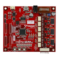
Fujitsu FR Family FR60 Lite User Manual (104 pages)
32-BIT MICROCONTROLLER bits pot red CAN motor board
Brand:
Fujitsu
| Category:
Computer Hardware
| Size: 2.49 MB
Table of Contents
Revision History
2
Note
3
Table of Contents
4
Introduction
10
Contact
11
Suppliers of the Parts/Materials
12
1 Setting up the Starter Kit
13
Table 1-1 Component List
13
Figure 1-1 External Board View
14
Table 1-2 Description of the Respective Board Parts
15
Figure 1-2 System Connection Diagram
16
Table 1-3 MB91F267N Pin Assignment
17
Setting up the PC
19
Downloading the Software
20
Installing a USB Driver
20
Figure 1-3 Downloading the USB Driver
20
Figure 1-4 Installing FT232R USB UART
21
Figure 1-5 Selecting the Search Locations
22
Figure 1-6 Completing the USB Serial Converter Installation
22
Figure 1-7 Installing USB Serial Port
23
Figure 1-8 Selecting the Search Locations
23
Figure 1-9 Completing the USB Serial Port Installation
24
Installing the Integrated Development Environment SOFTUNE (Bits Pot Dedicated Version)
25
Figure 1-10 SOFTUNE Setup Confirmation
25
Figure 1-11 Starting SOFTUNE Setup
25
Figure 1-12 Caution on SOFTUNE Setup
26
Figure 1-13 SOFTUNE Setup/License Agreement
26
Figure 1-14 SOFTUNE Setup/Version Information
27
Figure 1-15 SOFTUNE Setup/Selecting the Destination of Installation
27
Figure 1-16 SOFTUNE Setup/Selecting the Components
28
Figure 1-17 SOFTUNE Setup/Confirming the Installation Settings
28
Figure 1-18 SOFTUNE Setup/Completion
29
Installing PC Writer (Bits Pot Red Dedicated Version)
30
Figure 1-19 PC Writer/Installation Dialog
30
Figure 1-20 PC Writer/Setup Type
31
Figure 1-21 PC Writer/Ready to Install
31
Figure 1-22 Completing the PC Writer Installation
32
Configuring the Evaluation Board and Connecting It to the PC
33
Figure 1-23 MODE Selection
33
Figure 1-24 Connection between the PC and the Board
34
2 Running the Program
35
Executing in Single Chip Mode
36
Building a Project
36
Figure 2-1 Opening a Workspace
36
Figure 2-2 Selecting a Workspace
37
Figure 2-3 Building a Project
37
Writing the Program into the Microcontroller
38
Figure 2-4 Completing the Build
38
Figure 2-5 Opening the File to Write
38
Figure 2-6 Selecting the File to Write
39
Figure 2-7 Select the COM Port to be Used for the Writing
40
Figure 2-8 Checking the COM Port
41
Figure 2-9 Writing the Program
42
Figure 2-10 Completing the Program Writing
42
Debugging by Using Monitor Debugger
43
Writing Monitor Debugger into the Microcontroller
43
Figure 2-11 Opening the File to Write
43
Figure 2-12 Selecting the File to Write
44
Figure 2-13 Select the COM Port to be Used for the Writing
45
Figure 2-14 Checking the COM Port
46
Figure 2-15 Writing the Program
47
Figure 2-16 Completing the Program Writing
47
Activating SOFTUNE and Configuring the Debug Settings
48
Figure 2-17 Opening a Workspace
48
Figure 2-18 Selecting a Workspace
49
Figure 2-19 Building a Project
49
Figure 2-20 Completing the Build
50
Figure 2-21 Changing the Debug Settings
50
Figure 2-22 Starting the Debug Setting Wizard
51
Figure 2-23 Selecting the Debugger Type
51
Figure 2-24 Selecting the Device Type
52
Figure 2-25 Specifying a Batch File
52
Figure 2-26 Configuring the Target File Settings
53
Figure 2-27 Setting Setup File Selection
53
Figure 2-28 Completing the Setup Wizard
54
Figure 2-29 Start Debugging
54
Writing the Program into the Microcontroller
55
Figure 2-30 Showing the Commands Window
55
Figure 2-31 Inputting Commands
56
Figure 2-32 Completing the Program Writing
56
Loading the Target File
57
Figure 2-33 Loading the Target File
57
Running the Debugger
58
Figure 2-34 Setting Break Points
58
Figure 2-35 Running the Program
58
Notes on Monitor Debugger
59
Figure 2-36 Stopping the Program
59
3 Operation of the Sample Program
60
Bits Pot Red Single-Unit Operation
61
Figure 3-1 Single-Unit Operation/Controls and Mechanicals
61
Table 3-1 Single-Unit Operation/Descriptions of the Controls and Mechanicals
61
CAN Communication Operation (CAN Communication Operation with the Bits Pot White)
63
Figure 3-2 CAN Communication Operation/Controls and Mechanicals
63
Table 3-2 CAN Communication Operation/Descriptions of the Controls and Mechanicals
64
4 Try to Rotate the BLDC Motor
65
What Is the BLDC Motor
65
Figure 4-1 DC Motor/Bldc Motor Configuration Examples
65
How Does the BLDC Motor Rotate
66
Figure 4-2 Names of the Respective Elements
66
Figure 4-3 120° Conduction Method Time Chart
67
BLDC Motor Rotation Control by the Microcontroller
68
Figure 4-4 Motor Driver Circuit
68
Figure 4-5 Timer Control Registers
69
Table 4-1 Microcontroller Pin/Motor Driver Circuit Connections
69
Table 4-2 Functions Employed by the Motor Driving Macro
69
Table 4-3 Description of the Timer Control Registers and Setting Values
70
Figure 4-6 Output Compare Registers
71
Table 4-4 Description of the Output Compare Registers and Setting Values
72
Figure 4-7 Operation of the Free-Run Timer
73
Table 4-5 Correspondence between the Output Compare Values and the Switchings
73
Figure 4-8 U-High Output to Output Comparisons
74
Understanding and Running the Program for the BLDC Motor Operation
75
Figure 4-9 Motor Operation Flowchart
75
Figure 4-10 Operation Mode Settings
76
Figure 4-11 Main Function
76
Figure 4-12 SW2 Interrupt
77
Figure 4-13 Free-Run Timer Interrupt
77
Handling Controls of the BLDC Motor
78
Figure 4-14 Motor Controls Flowchart
78
Figure 4-15 Rotation Speed Control
79
Figure 4-16 Brake Control
80
Figure 4-17 Rotation Direction Control
81
Fujitsu FR Family FR60 Lite User Manual (26 pages)
Brand:
Fujitsu
| Category:
Adapter
| Size: 0.56 MB
Table of Contents
User Guide
1
Revision History
2
Warranty and Disclaimer
3
Table of Contents
4
Contents
4
1 Overview
5
Abstract
5
General Description
6
Functional Restrictions
7
2 Installation
9
3 Switches and Jumpers
10
Level Shifter Switches and Jumpers Overview
10
Level-Shifter Direction Control Jumper
11
Bus Control Jumpers
12
Port 17 Jumpers (APIX AIC Link)
16
Default Jumper Setting
17
4 Mechanical Dimensions
19
5 Cpld
20
CPLD Verilog Code
20
CPLD Constraints
22
CPLD Programming Jumper (J491)
22
6 Information in the Www
23
7 China-Rohs Regulation
24
8 Recycling
26
Advertisement
Related Products
Fujitsu F2MCTM-16LX
Fujitsu FMC-16LX/FR
Fujitsu F2MC-8L F202RA
Fujitsu F2MC-8L MB89202
Fujitsu F2 MC-8FX Family
Fujitsu FM3 family
Fujitsu FibreCAT TXF
Fujitsu F2MC-16FR
Fujitsu F2MC-16FX MB2198
Fujitsu F2MC-8FX MB2146-222
Fujitsu Categories
Air Conditioner
Laptop
Server
Scanner
Storage
More Fujitsu Manuals
Login
Sign In
OR
Sign in with Facebook
Sign in with Google
Upload manual
Upload from disk
Upload from URL