Table of Contents
Advertisement
Quick Links
Advertisement
Table of Contents

Related Manuals for Motorola MVME177


Summary of Contents for Motorola MVME177
- Page 1 MVME177 Single Board Computer Installation and Use Manual VME177A/IH2...
- Page 2 Motorola, Inc. assumes no liability resulting from any omissions in this document, or from the use of the information obtained therein. Motorola reserves the right to revise this document and to make changes from time to time in the content hereof without obligation of Motorola to notify any person of such revision or changes.
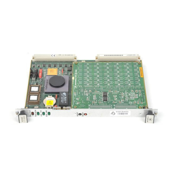
- Page 3 The MVME177 UserÕs Manual provides general information, hardware preparation and installation instructions, operating instructions, and functional description for the MVME177 Single Board Computer (referred to as MVME177 throughout this manual). The information contained in this manual applies to the following...
- Page 4 The computer programs stored in the Read Only Memory of this device contain material copyrighted by Motorola Inc., Þrst published 1990, and may be used only under a license such as the License for Computer Programs (Article 14) contained in Motorola's Terms and Conditions of Sale, Rev. 1/79.
- Page 5 Motorola, Inc. assumes no liability for the customer's failure to comply with these requirements. The safety precautions listed below represent warnings of certain dangers of which Motorola is aware. You, as the user of the product, should follow these warnings and all other safety precautions necessary for the safe operation of the equipment in your operating environment.
-
Page 7: Table Of Contents
Manual Terminology 1-12 Introduction 2-1 Unpacking Instructions 2-1 Overview of Start-up Procedure 2-2 Hardware Preparation 2-4 Setup Instructions 2-10 MVME177 Module Installation Instructions 2-12 System Considerations 2-15 Introduction 3-1 Controls and Indicators 3-1 ABORT Switch S1 3-1 RESET Switch S2 3-2... - Page 8 SRAM 4-7 Onboard DRAM 4-9 Battery Backed Up RAM and Clock 4-10 VMEbus Interface 4-11 I/O Interfaces 4-11 Serial Port Interface 4-12 Parallel Port Interface 4-14 Ethernet Interface 4-15 SCSI Interface 4-16 SCSI Termination 4-16 Local Resources 4-16 Programmable Tick Timers 4-17 Watchdog Timer 4-17 Software-Programmable Hardware Interrupts 4-17 Local Bus Time-out 4-18...
- Page 9 Disk I/O Support B-13 Blocks Versus Sectors B-13 Device Probe Function B-15 Disk I/O via 177Bug Commands B-16 IOI (Input/Output Inquiry) B-16 IOP (Physical I/O to Disk) B-16 IOT (I/O Teach) B-17 IOC (I/O Control) B-17 BO (Bootstrap Operating System) B-17 BH (Bootstrap and Halt) B-17 Disk I/O via 177Bug System Calls B-17 Default 177Bug Controller and Device Parameters B-19...
- Page 10 177Bug Generalized Exception Handler B-42 Floating Point Support B-44 Single Precision Real B-45 Double Precision Real B-46 Extended Precision Real B-46 Packed Decimal Real B-46 ScientiÞc Notation B-47 Additions to FLASH Commands B-47 Flash Test ConÞguration Acceptable Entries B-48 Erase Test B-48 Flash Fill Test B-48 Flash Patterns Test B-49 Default Flash Test ConÞguration B-50...
-
Page 11: List Of Figures
List of Figures MVME177 Switches, Headers, Connectors, Polyswitches, and LEDs 2-5 MVME177 Block Diagram 4-3... -
Page 12: List Of Tables
List of Tables MVME177 Model Designations 1-1 MVME177 Features 1-2 MVME177 SpeciÞcations 1-4 Start-up Overview 2-2 ConÞguring MVME177 Headers 2-6 Local Bus Memory Map 3-5 Local I/O Devices Memory Map 3-6 EPROM and Flash Control and ConÞguration 4-5 Diagnostic Test Groups B-26... -
Page 13: Introduction
Functional description for the MVME177 series of Single Board Computers (referred to as the MVME177 throughout this manual). Model Designations The MVME177 is available in the models listed in Table 1 - 1. Table 1-1. MVME177 Model Designations Model Number Speed... -
Page 14: Features
General Information Features Features of the MVME177 are listed in the following table: Table 1-2. MVME177 Features Feature Description Microprocessor MC68060 at 50 MHz (MVME177-00x) or 60 MHz (MVME177-01x) DRAM 4/8/16/32/64/128/256MB with ECC protection Flash Memory 4MB in four Intel 28F008SA chips with software control write... -
Page 15: Cooling Requirements
Specifications Specifications General specifications for the MVME177 are listed in Table 1-3. The following sections detail cooling requirements and FCC compliance. Cooling Requirements The Motorola MVME177 VMEmodule is specified, designed, and tested to operate reliably with an incoming air temperature range from 0û... - Page 16 Refer to the Cooling Requirements section in the General Information chapter for temperature qualification information for the system board platform. Table 1-3. MVME177 Specifications Characteristics SpeciÞcations Power requirements +5 Vdc (± 5%), 4.5 A (typical), 6.0 A (max.)
-
Page 17: Fcc Compliance
General Description FCC Compliance The MVME177 was tested in an FCC-compliant chassis, and meets the requirements for Class A equipment. FCC compliance was achieved under the following conditions: 1. Shielded cables on all external I/O ports. 2. Cable shields connected to earth ground via metal shell connectors bonded to a conductive module front panel. - Page 18 128KB of static RAM (with optional battery backup), and VMEbus system controller. The I/O on the MVME177 is connected to the VMEbus P2 connector. The main board is connected through a P2 transition board and cables to the transition boards. The MVME177 supports...
- Page 19 General Description VMEbus interrupter VMEbus system controller VMEbus interrupt handler VMEbus requester Processor-to-VMEbus transfers can be: VMEchip2 DMA transfers to the VMEbus, however, can be: D16/BLT D32/BLT D64/MBLT The PCCchip2 ASIC provides: Two tick timers Interface to the LAN chip SCSI chip Serial port chip Parallel (printer) port...
-
Page 20: Equipment Required
Connecting cables P2 adapter Operating system The MVME177Bug debug monitor firmware (177Bug) is provided in the two EPROMs in sockets on the MVME177 main module. It provides: Over 50 debug, up/downline load, and disk bootstrap load commands Full set of onboard diagnostics... -
Page 21: Related Documentation
Other tools and applications Contact your local Motorola sales office for more details. Related Documentation The following publications are applicable to the MVME177 and may provide additional helpful information. If not shipped with this product, they may be purchased by contacting your local Motorola sales office. - Page 22 General Information Motorola Publication Document Title Number 177Bug Diagnostics UserÕs Manual V177DIAA/UM Debugging Package for Motorola 68K CISC CPUs User's Manual 68KBUG1/D and 68KBUG2/D Single Board Computers SCSI Software User's Manual SBCSCSI/D Single Board Computers Programmer's Reference Guide VMESBCA/PG1 VMESBCA/PG2...
-
Page 23: Support Information
DS1643 Nonvolatile Timekeeping RAM, Dallas Semiconductor Data Manual, 4401 South Beltwood Parkway, Dallas, Texas 75244-3292. Support Information You can obtain connector interconnect signal information, parts lists, and schematics for the MVME177 free of charge by contacting your local Motorola sales office. 1-11... -
Page 24: Manual Terminology
General Information Manual Terminology Throughout this manual, a convention is used which precedes data and address parameters by a character identifying the numeric format as follows: dollar speciÞes a hexadecimal character percent speciÞes a binary number & ampersand speciÞes a decimal number Unless otherwise specified, all address references are in hexadecimal. -
Page 25: Introduction
2Hardware Preparation and Installation Introduction This chapter provides the following for the MVME177: Unpacking instructions Hardware preparation Installation instructions The MVME712x transition module hardware preparation is provided in separate manuals. Refer to Related Documentation in Chapter 1. Unpacking Instructions Note... -
Page 26: Overview Of Start-Up Procedure
Caution notes before beginning. Table 2-1. Start-up Overview What you will need to do ... Refer to ... On page ... Set jumpers on your MVME177 Hardware Preparation module. Ensure that EPROM devices are Hardware Preparation properly installed in the sockets. - Page 27 Note that the debugger prompt Installation Instructions 2-12 appears. Debugger General Information. You may also wish to obtain the Debugging Package for Motorola 68K CISC CPUs UserÕs Manual and the 177Bug Diagnostics UserÕs Manual, listed in Related Documentation Initialize the clock.
-
Page 28: Hardware Preparation
Some options cannot be done in software, so are done by jumpers on headers. Most other modifications are done by setting bits in control registers after the MVME177 has been installed in a system. (The MVME177 registers are described in Chapter 4, and/or in the Single Board Computers Programmer's Reference Guide as listed in Related Documentation in Chapter 1). - Page 29 Hardware Preparation POLYSWITCH MVME FAIL STAT RUN SCON +12V SCSI VME ABORT RESET Figure 2-1. MVME177 Switches, Headers, Connectors, Polyswitches, and LEDs...
- Page 30 Hardware Preparation and Installation Table 2-2. Configuring MVME177 Headers Header Header Number Description ConÞguration Jumpers Notes GPI0 - GPI2: 1 -- 2 (GPI0) GPI0 User-deÞnable 3 -- 4 (GPI1) GPI1 5 -- 6 (GPI2) GPI2 General GPI3: Reserved 1, 2...
- Page 31 Hardware Preparation Table 2-2. Configuring MVME177 Headers (Continued) Header Header Number Description ConÞguration Jumpers Notes System 1 -- 2 controller (Factory conÞguration) Auto system System controller 2 -- 3 controller header Not system controller None THERM1 Thermal sensing Connected to...
- Page 32 VMEchip2). The bit values are read as a 1 when the jumper is off, and as a 0 when the jumper is on. On the MVME177, pins 7 and 8 (bit 3) are removed for board ID and the bit value is reserved.
- Page 33 J6. If set for AUTO SCON, the MVME177 determines if it is the system controller by its position on the bus. If the MVME177 is in the Þrst slot from the left, it conÞgures itself as the system controller. When the MVME177 is system controller, the LED is turned on.
-
Page 34: Setup Instructions
Hardware Preparation and Installation Setup Instructions Even though the MVME177Bug EPROMs are installed on the MVME177 module in the factory, follow this setup procedure for 177Bug to operate properly with the MVME177. Inserting or removing modules while power is applied could damage module components. - Page 35 Table 2-2. 3. Be sure that the two 256K x 16 177Bug EPROMs are installed in proper sockets on the MVME177 module. Install the odd label (such as B01) EPROM in socket XU1 (for Least Significant Words), and install the even label (such as B02) EPROM in XU2 (for Most Significant Words).
-
Page 36: Mvme177 Module Installation Instructions
MVME712M which has a double-wide front panel. 4. Carefully slide the MVME177 module into the card slot. Be sure the module is seated properly into the P1 and P2 connectors on the backplane. Do not damage or bend connector pins. - Page 37 RFI emissions. 5. Remove IACK and BG jumpers from the header on the chassis backplane for the card slot in which the MVME177 is installed. 6. Connect the P2 Adapter Board and specified cable(s) to the...
- Page 38 MVME177 CD2401 Serial Controller Chip (SCC), or by using the 177Bug PF command. Note that the MVME177 also contains a parallel port. To use a parallel device, such as a printer, with the MVME177, connect it to the "printer" port at P2 through an MVME712x transition module.
-
Page 39: System Considerations
D for the environment parameters. System Considerations The MVME177 draws power from both P1 and P2 of the VMEbus backplane. P2 is also used for the upper 16 bits of data for 32-bit transfers, and for the upper 8 address lines for extended addressing mode. - Page 40 If the MVME177 attempts to access offboard resources in a nonexistent location, and is not system controller, and if the system does not have a global bus time-out, the MVME177 waits forever for the VMEbus cycle to complete. This causes the system to hang up.
- Page 41 LED (DS1) on the MVME712M front panel lights when LAN power is available, indicating that the polyswitch is good. The MVME177 provides SCSI terminator power through a diode and a 1 amp polyswitch F1 located on the P2 Adapter Board. If the polyswitch is blown (i.e., open), the SCSI devices may not operate...
- Page 42 Hardware Preparation and Installation 2-18...
-
Page 43: Introduction
Controls and indicators Memory maps Software initialization of the module Controls and Indicators On the front panel of the MVME177 module are the following: ABORT and RESET switches FAIL, STAT, RUN, SCON, LAN,+12V (LAN power), SCSI, and VME indicators ABORT Switch S1 When enabled by software, the recessed front panel ABORT switch generates an interrupt at a user-programmable level. -
Page 44: Reset Switch S2
Operating Instructions RESET Switch S2 The recessed front panel RESET switch resets all onboard devices, and drives SYSRESET* if the board is system controller. The RESET switch may be disabled by software. The VMEchip2 includes both a global and a local reset driver. When the chip operates as the VMEbus system controller, the reset driver provides a global system reset by asserting the VMEbus signal SYSRESET*. -
Page 45: Front Panel Indicators (Ds1 - Ds4)
Controls and Indicators Front Panel Indicators (DS1 - DS4) There are eight LEDs on the MVME177 front panel: FAIL, STAT, RUN, SCON, LAN, +12V (LAN power), SCSI, and VME. The purpose of each LED is as follows: The red FAIL LED (part of DS1) lights when the BRDFAIL... -
Page 46: Memory Maps
The memory map of devices that respond to the normal address range is shown in the following tables. The normal address range is defined by the Transfer Type (TT) signals on the local bus. On the MVME177, Transfer Types 0, 1, and 2 define the normal address range. Table 3-1. - Page 47 (DRAM or SRAM) can be mapped in this range ($00000000 through $003FFFFF). The VMEchip2 and DRAM map decoders are disabled by a local bus reset. On the MVME177, the Flash/EPROM memory is mapped at $00000000 through $003FFFFF by hardware default through the VMEchip2.
- Page 48 TEA signal. 6. The SRAM has optional battery backup on the MVME177. The following table focuses on the Local I/O Devices portion of the local bus Main Memory Map.
- Page 49 For a more detailed memory map, refer to the following detailed peripheral device memory maps. 2. On the MVME177 this area does not return an acknowledge signal. If the local bus timer is enabled, the access times out and terminates by a TEA signal.
-
Page 50: Software Initialization
8. Port commands to the 82596CA must be written as two 16-bit writes: upper word first and lower word second. 9. The CD2401 appears repeatedly from $FFF45200 to $FFF45FFF on the MVME177. If the local bus timer is enabled, the access times out and terminates by a TEA signal. Software Initialization... - Page 51 Any VMEbus access to the MVME177 while it is in the reset state is ignored. If a global bus timer is enabled, a bus error is generated.
- Page 52 Operating Instructions 3-10...
-
Page 53: Introduction
Descriptions of the other blocks of the MVME177, including programmable registers in the ASICs and peripheral chips, are given in the Single Board Computers Programmer's Reference Guide. Refer to it for the rest of the functional description of the MVME177 module. MVME177 Functional Description The MVME177 is a high functionality VMEbus single board computer designed around the MC68060 chip. - Page 54 Functional Description local bus to communicate. The local bus is arbitrated by priority type arbiter and the priority of the local bus masters from highest to lowest is: 82596CA LAN CD2401 serial (through the PCCchip2) 53C710 SCSI VMEbus In the general case, any master can access any slave; however, not all combinations pass the common sense test.
- Page 55 MVME177 Functional Description Figure 4-1. MVME177 Block Diagram...
-
Page 56: Mc68060 Mpu
MC68060 user's manual for more information. Flash Memory and EPROM Flash Memory The MVME177 includes four 28F008SA Flash memory devices. The Flash devices provide 4MB of ROM at address $FF800000- $FFBFFFFF. The Flash is organized as one 32-bit bank for 32-bit code execution from the processor. - Page 57 Flash is accessable at addresses $200000 through $3FFFFF, depending on the condition of the VMEchip2 GPIO2 bit. Because the MVME177 uses 1M x 8-bit Flash memory devices and EPROMs with no download ROM, the software programs the VMEchip2 ROM0 and REV EROM bits properly so that the Flash/EPROM appears at address $0 after powerup.
-
Page 58: Eprom
Functional Description The MVME177 implements Flash write protection through clearing a control bit (GPIO1) in the GPIO register in the VMEchip2, to enable write by the software after download process/ programming is completed. EPROM There are two 44-pin PLCC/CLCC EPROM sockets for SGS- Thompson M27C4002 (256K x 16) or AMD 27C4096 type EPROMs. -
Page 59: Sram
MVME177. The battery supplies VCC to the SRAMs when main power is removed. Each time the MVME177 is powered up, the DS1210S checks the power source. If the voltage of the backup source is less than two... - Page 60 Optionally, the MVME177 provides jumpers that allow the power source of the DS1210S to connect to the VMEbus +5 V STDBY pin or the onboard battery.
-
Page 61: Onboard Dram
To remove the battery from the module, carefully pull the battery from the socket. Onboard DRAM The MVME177 onboard DRAM is located on a mezzanine board. The mezzanine boards use error checking and correction (ECC) protection to correct single-bit errors and detect double-bit errors. -
Page 62: Battery Backed Up Ram And Clock
10 initialization cycles are performed to each bank of RAM. Battery Backed Up RAM and Clock The DS1643/MK48T08 RAM and clock chip is used on the MVME177. This chip provides the following items, all in one 28-pin package: Time of day clock Oscillator... -
Page 63: Vmebus Interface
The local bus to VMEbus interface, the VMEbus to local bus interface, and the local-VMEbus DMA controller functions on the MVME177 are provided by the VMEchip2. The VMEchip2 can also provide the VMEbus system controller functions. Refer to the VMEchip2 in the Single Board Computers Programmer's Reference Guide for detailed programming information. -
Page 64: Serial Port Interface
Functional Description Parallel (printer) port Ethernet transceiver interface SCSI mass storage interface Serial Port Interface The CD2401 serial controller chip (SCC) is used to implement the four serial ports. The serial ports support the standard baud rates (110 to 38.4K baud). The four serial ports are different functionally because of the limited number of pins on the P2 I/O connector. - Page 65 MVME712x should be used to convert the I/O connector pinout to industry-standard connectors. Note The MVME177 board hardware ties the DTR signal from the CD2401 to the pin labeled RTS at connector P2. Likewise, RTS from the CD2401 is tied to DTR on P2.
-
Page 66: Parallel Port Interface
Functional Description Parallel Port Interface The PCCchip2 provides an 8-bit bidirectional parallel port. All eight bits of the port must be either inputs or outputs (no individual selection). In addition to the 8 bits of data, there are two control pins and five status pins. -
Page 67: Ethernet Interface
Every MVME177 is assigned an Ethernet Station Address. The address is $08003E2xxxxx, where xxxxx is the unique 5-nibble number assigned to the board (i.e., every MVME177 has a different value for xxxxx). Each module has an Ethernet Station Address displayed on a label attached to the VMEbus P2 connector. -
Page 68: Scsi Interface
SCSI Termination The system configurer must ensure that the SCSI bus is properly terminated at both ends. On the MVME177, sockets are provided for the terminators on the P2 transition board. If the SCSI bus ends at the P2 transition board, then termination resistors must be installed on the P2 transition board. -
Page 69: Programmable Tick Timers
MVME177 Functional Description Local bus time-out Note The time basis for all local resources is set by Prescaler register(s). Refer to the Single Board Computers Programmer's Reference Guide for detailed programming information. Programmable Tick Timers Four 32-bit programmable tick timers with 1 µs resolution are... -
Page 70: Module Identiþcation
Software distinguishes between an MVME177 module and an MVME176 module by use of the I/O control register (GPI) bit 3. On an MVME177, the I/O control register (GPI) bit 3 is out (open) for a ÒhighÓ (one). On an MVME176, the I/O control register (GPI) bit 3 is hardwired in (shorted) for a ÒlowÓ... -
Page 71: Rom Cycle Times
Computers Programmer's Reference Guide. SCSI Transfers The MVME177 includes a SCSI mass storage bus interface with DMA controller. The SCSI DMA controller uses a FIFO buffer to interface the 8-bit SCSI bus to the 32-bit local bus. The FIFO buffer allows the SCSI DMA controller to efficiently transfer data to the local bus in four longword bursts. -
Page 72: Lan Dma Transfers
Remote Status and Control The remote status and control connector, J3, is a 20-pin connector located behind the front panel of the MVME177. It provides system designers the flexibility to access critical indicator and reset functions. This allows a system designer to construct a RESET/ABORT/LED panel that can be located remotely from the MVME177. -
Page 73: Introduction
AEIA-232-D Interconnections Introduction The EIA-232-D standard is the most widely used terminal/computer and terminal/modem interface, and yet it is not fully understood. This may be because not all the lines are clearly defined, and many users do not see the need to follow the standard in their applications. - Page 74 EIA-232-D Interconnections Table A-1. EIA-232-D Interconnections Signal Number Mnemonic Signal Name and Description Not used. TRANSMIT DATA. Data to be transmitted; input to the modem from the terminal. RECEIVE DATA. Data which is demodulated from the receive line; output from the modem to the terminal. REQUEST TO SEND.
-
Page 75: Levels Of Implementation
Levels of Implementation Table A-1. EIA-232-D Interconnections (Continued) Signal Number Mnemonic Signal Name and Description RING INDICATOR. Output from the modem to the terminal; indicates to the terminal that an incoming call is present. The terminal causes the modem to answer the phone by carrying DTR true while RI is active. -
Page 76: Signal Adaptations
EIA-232-D Interconnections Signal Adaptations One set of handshaking signals frequently implemented are RTS and CTS. CTS is used in many systems to inhibit transmission until the signal is high. In the modem application, RTS is turned around and returned as CTS after 150 microseconds. RTS is programmable in some systems to work with the older type 202 modem (half duplex). - Page 77 Levels of Implementation 6850 39kΩ -12V CONNECTOR +12V LS08 TERMINAL 470Ω 470Ω 470Ω OPTIONAL HARDWARE TRANSPARENT SIG GND MODE CHASSIS GND LOGIC LS08 +12V SIG GND 470Ω 6850 CONNECTOR 39kΩ -12V MODEM HOST 470Ω SYSTEM +12V 39kΩ 470Ω -12V +12V 39kΩ...
- Page 78 EIA-232-D Interconnections Figure A-2 shows a way of wiring an EIA-232-D connector to enable a computer to connect to a basic terminal with only three lines. This is feasible because most terminals have a DTR signal that is ON, and which can be used to pull up the CTS, DCD, and DSR signals. Two of these connectors wired back-to-back can be used.
-
Page 79: Proper Grounding
Levels of Implementation Proper Grounding Another subject to consider is the use of ground pins. There are two pins labeled GND. Pin 7 is the SIGNAL GROUND and must be connected to the distant device to complete the circuit. Pin 1 is the CHASSIS GROUND, but it must be used with care. - Page 80 EIA-232-D Interconnections...
-
Page 81: Overview Of M68000 Firmware
Portability Ease of maintenance This member of the M68000 firmware family is implemented on the MVME177 Single Board Computer, and is known as the MVME177Bug, or simply 177Bug. Description of 177Bug The 177Bug package is a powerful evaluation and debugging tool for systems built around the MVME177 CISC-based microcomputers. - Page 82 177Bug, depending on the outcome of the user program. If you have used one or more of Motorola's other debugging packages, you will find the CISC 177Bug very similar. Considerable effort has also been made to make the interactive commands more consistent.
-
Page 83: 177Bug Implementation
Eight bits per character One stop bit per character Parity disabled (no parity) Baud rate 9600 baud (default baud rate of MVME177 ports at power-up) After power-up, the baud rate of the debug port can be reconfigured by using the Port Format (PF) command of the 177Bug debugger. - Page 84 Programming of the Boot delay Refer to the ENV command in the Commands Table for more details. Although streaming tape can be used to autoboot, the same power supply must be connected to the: Caution Streaming tape drive Controller MVME177...
-
Page 85: Romboot
Power must have just been applied (but the ENV command can change this to also respond to any reset) Your routine must be located within the MVME177 ROM memory map (but the ENV command can change this to any other portion of the onboard memory, or even offboard... -
Page 86: Network Boot
For complete details on how to use ROMboot, refer to the Debugging Package for Motorola 68K CISC CPUs User's Manual. Network Boot Network Auto Boot is a software routine contained in the 177Bug EPROMs that provides a mechanism for booting an operating system using a network (local Ethernet interface) as the boot device. -
Page 87: Restarting The System
Restarting the System Network Auto Boot is controlled by parameters contained in the NIOT and ENV commands. These parameters allow: Selection of specific boot devices Selection of systems Selection of files Programming of the Boot delay Refer to the ENV and NIOT commands in the Commands Table in this Appendix for more details. -
Page 88: Reset
Abort You can initiate an abort by pressing and releasing the ABORT switch on the MVME177 front panel. If an abort is initiated while executing a user program (running target code), a ÒsnapshotÓ of the processor state is captured and stored in the target registers. For... -
Page 89: Break
Restarting the System program that is being debugged. Abort should be used to regain control if the program gets caught in a loop, etc. The target PC and register contents assist you in locating the malfunction. Pressing and releasing the ABORT switch generates a local board condition that causes: A processor interrupt (if enabled) The target registers (reflecting the machine state at the time... -
Page 90: Sysfail* Assertion/Negation
Debugger General Information SYSFAIL* Assertion/Negation Upon a reset/power-up condition the debugger asserts the VMEbus SYSFAIL* line (refer to the VMEbus specification). SYSFAIL* stays asserted if any of the following has occurred: Confidence test failure NVRAM checksum error NVRAM low battery condition Local memory configuration status Self test (if system mode) has completed with error MPU clock speed calculation failure... -
Page 91: Memory Requirements
Regardless of where the onboard RAM is located, the first 64KB is used for 177Bug stack and static variable space and the rest is reserved as user space. Whenever the MVME177 is reset: Target PC is initialized to the address corresponding to the... -
Page 92: Terminal Input/Output Control
Debugger General Information Terminal Input/Output Control When entering a command at the prompt, the following control codes may be entered for limited command line editing. Note The presence of the caret ( ^ ) before a character indicates that the Control (CTRL) key must be held down while striking the character key (cancel line) The cursor is backspaced to the beginning of the line. -
Page 93: Disk I/O Support
Disk I/O Support (default). These characters are initialized to ^S and ^Q respectively by 177Bug, but you may change them with the PF command. In the initialized (default) mode, operation is as follows: (wait) Console output is halted. (resume) Console output is resumed. Disk I/O Support 177Bug can initiate disk input/output by communicating with intelligent disk controller modules over the VMEbus. - Page 94 Debugger General Information The sector defines the unit of information for the media itself, as viewed by the controller. The sector size varies for different controllers, and the value for a specific device can be displayed and changed with the IOT command. B-14...
-
Page 95: Device Probe Function
Disk I/O Support When a disk transfer is requested: Start and size of the transfer is specified in blocks 177Bug translates this into an equivalent sector specification Passes the sector specification on to the controller to initiate the transfer If the conversion from blocks to sectors yields a fractional sector count, an error is returned and no data is transferred. -
Page 96: Disk I/O Via 177Bug Commands
The 177Bug commands listed in the following paragraphs are provided for disk I/O. Detailed instructions for their use are found in the Debugging Package for Motorola 68K CISC CPUs User's Manual. When a command is issued to a particular controller LUN and device LUN, these LUNs are remembered by 177Bug so that the next disk command defaults to use the same controller and device. -
Page 97: Iot (I/O Teach
Disk I/O Support IOT (I/O Teach) IOT allows you to change any configurable parameters and attributes of the device. In addition, it allows you to view the controllers available in the system. IOC (I/O Control) IOC allows you to send command packets as defined by the particular controller directly. - Page 98 Send it to the specified device Refer to the system call descriptions in the Debugging Package for Motorola 68K CISC CPUs User's Manual for details on the format and construction of these standardized ÒuserÓ packets. The packets which a controller module expects to receive vary from controller to controller.
-
Page 99: Default 177Bug Controller And Device Parameters
Disk I/O Support Default 177Bug Controller and Device Parameters 177Bug initializes the parameter tables for a default configuration of controllers and devices (refer to Appendix C). If the system needs to be configured differently than this default configuration (for example, to use a 70MB Winchester drive where the default is a 40MB Winchester drive), then these tables must be changed. -
Page 100: Intel 82596 Lan Coprocessor Ethernet Driver
Debugger General Information The first phase: the diskless remote node discovers its network identify and the name of the file to be booted The second phase: the diskless remote node reads the boot file across the network into its memory The various modules (capabilities) and the dependencies of these modules that support the overall network boot function are described in the following paragraphs... -
Page 101: Rarp/Arp Protocol Modules
Disk I/O Support RARP/ARP Protocol Modules The Reverse Address Resolution Protocol (RARP) basically consists An identity-less node broadcasting a ÒwhoamiÓ packet onto the Ethernet The node awaiting an answer The RARP server filling an Ethernet reply packet with the target's Internet Address The RARP server sending it to the node The Address Resolution Protocol (ARP) basically provides a method of converting protocol addresses (e.g., IP addresses) to... -
Page 102: Network Boot Control Module
177Bug returns an error code whenever an attempted network operation is unsuccessful. Multiprocessor Support The MVME177 dual-port RAM feature makes the shared RAM available to remote processors as well as to the local processor. This can be done by either of the following two methods. Either method can be enabled/disabled by the ENV command as its Remote Start Switch Method. - Page 103 Multiprocessor Support The status codes stored in the MPCR are of two types: Status returned (from the monitor) Status set (by the bus master) The status codes that may be returned from the monitor are: (HEX 00) Wait. Initialization not yet complete. ASCII R (HEX 52) Ready.
-
Page 104: Gcsr Method
RAM location. GCSR Method A remote processor can initiate program execution in the local MVME177 dual-port RAM by issuing a remote GO command using the VMEchip2 Global Control and Status Registers (GCSR). The remote GO command causes the following sequence:... -
Page 105: Diagnostic Facilities
Diagnostic Facilities and Status Registers (LCSR) of the MVME177. The execution address is formed by reading the GCSR general purpose registers in the following manner: GPCSR0 used as the upper 16 bits of the address GPCSR1 used as the lower 16 bits of the address... - Page 106 Debugger General Information Table B-1. Diagnostic Test Groups Test Group Description Local RAM Tests SRAM Static RAM Tests MK48T0x Real-Time Clock Tests PCC2 Peripheral Channel Controller Tests MCECC Memory Board Tests MEMC1 MC040 Memory Controller 1 ASIC Tests MEMC2 MC040 Memory Controller 2 ASIC Tests ST2401 CD2401 Serial Port Tests CMMU...
-
Page 107: Using The 177Bug Debugger
Using the 177Bug Debugger Using the 177Bug Debugger Entering Debugger Command Lines 177Bug is command-driven and performs its various operations in response to user commands entered at the keyboard. When the debugger prompt ( ) appears on the terminal screen, then 177-Bug>... -
Page 108: Syntactic Variables
Debugger General Information The commands are shown using a modified Backus-Naur form syntax. The metasymbols used are: boldface strings A boldface string is a literal such as a command or a program name, and is to be typed just as it appears. italic strings An italic string is a Òsyntactic variableÓ... -
Page 109: Expression As A Parameter
Using the 177Bug Debugger Expression as a Parameter An expression can be one or more numeric values separated by the arithmetic operators: Plus (+) Minus (-) Multiplied by (*) Divided by (/) Logical AND (&) Shift left (<<) Shift right (>>) Numeric values may be expressed in either: Hexadecimal Decimal... - Page 110 Debugger General Information A numeric value may also be expressed as a string literal of up to four characters. The string literal must begin and end with the single quote mark ('). The numeric value is interpreted as the concatenation of the ASCII values of the characters. This value is right-justified, as any other numeric value would be.
-
Page 111: Address As A Parameter
Using the 177Bug Debugger Address as a Parameter Many commands use ADDR as a parameter. The syntax accepted by 177Bug is similar to the one accepted by the MC68060 one-line assembler. All control addressing modes are allowed. An Òaddress + offset registerÓ mode is also provided. Address Formats Table B-2 summarizes the address formats which are acceptable for address parameters in debugger command lines. -
Page 112: Offset Registers
Debugger General Information Ñ Address register n. Ñ Index register n (An or Dn). Ñ Displacement (any valid expression). Ñ Base displacement (any valid expression). Ñ Outer displacement (any valid expression). Ñ Register number (0 to 7). Ñ Offset register n. In commands with RANGE specified as ADDR DEL Note ADDR, and with size option W or L chosen, data at the... - Page 113 Using the 177Bug Debugger Example: A portion of the listing file of an assembled, relocatable module is shown below: * MOVE STRING SUBROUTINE 0 00000000 48E78080 MOVESTR MOVEM.L D0/A0,—(A7) 0 00000004 4280 CLR.L 0 00000006 1018 MOVE.B (A0)+,D0 0 00000008 5340 SUBQ.W #1,D0 0 0000000A 12D8...
-
Page 114: Port Numbers
MVME177 P2 connector). Sometimes known as the Òconsole portÓ, it is used for interactive user input/output by default. 2. MVME177 EIA-232-D (Terminal Port 1 or 01) (PORT 2 on the MVME177 P2 connector). Sometimes known as the Òhost portÓ, this is the default for: Ð... -
Page 115: Entering And Debugging Programs
MVME177 port 1. (Hardware configuration details are in the section on Installation and Start-Up in Chapter 3.) The file is downloaded from the host to MVME177 memory by the Load (LO) command. Another way is by reading in the program from disk, using one of... -
Page 116: Calling System Utilities From User Programs
You can access various 177Bug routines via one of the MC68060 TRAP instructions, using vector #15. Refer to the Debugging Package for Motorola 68K CISC CPUs User's Manual for details on the various TRAP #15 utilities available and how to invoke them from within a user program. -
Page 117: Hardware Functions
Preserving the Debugger Operating Environment Allocates space for the system stack Initializes the system stack pointer to the top of this area With the exception of the first 1024-byte vector table area, you must be extremely careful not to use the above-mentioned memory areas for other purposes. - Page 118 Debugger General Information Table B-3. Exception Vectors Used by 177Bug Vector Offset Exception 177Bug Facility Illegal instruction Breakpoints (used by GO, GN, GT) Trace Trace operations (such as T, TC, TT) $80-$B8 TRAP #0 - #14 Used internally TRAP #15 System calls $Note Level 7 interrupt...
-
Page 119: Using 177Bug Target Vector Table
Preserving the Debugger Operating Environment Notice that the value of the target stack pointer register (A7) has not changed even though a trace exception has taken place. Your program may either use the exception vector table provided by 177Bug or it may create a separate exception vector table of its own. The two following sections detail these two methods. -
Page 120: Creating A New Vector Table
Debugger General Information Creating a New Vector Table Your program may create a separate vector table in memory to contain its exception vectors. If this is done, the program must change the value of the VBR to point to the new vector table. In order to use the debugger facilities you can copy the proper vectors from the 177Bug vector table into the corresponding vector locations in your program vector table. - Page 121 Preserving the Debugger Operating Environment It may happen that your program uses one or more of the exception vectors that are required for debugger operation. Debugger facilities may still be used, however, if your exception handler can determine when to handle the exception itself and when to pass the exception to the debugger.
-
Page 122: 177Bug Generalized Exception Handler
Debugger General Information 177Bug Generalized Exception Handler The 177Bug has a generalized exception handler which it uses to handle all of the exceptions not listed in Table B-3. For all these exceptions, the target stack pointer is left pointing to the top of the exception stack frame created. - Page 123 Preserving the Debugger Operating Environment 177Bug> =000E0000 SR =2700=TR:OFF_S._7_..=00000000 SSP* =00010000 USP =00010000 SFC =1=UD =1=UD CACR =00000000=D:.._B:..._I:... =04300000 =00000000 D1 =00000000 D2 =00000000 D3 =00000000 =00000000 D5 =00000000 D6 =00000000 D7 =00000000 =00000000 A1 =00000000 A2 =00000000 A3 =00000000 =00000000 A5 =000C0000 A6...
-
Page 124: Floating Point Support
Debugger General Information Floating Point Support The floating point unit (FPU) of the MC68060 microprocessor chip is supported in 177Bug. For MVME177Bug, the commands: have been extended to allow display and modification of floating point data in registers and in memory. Floating point instructions can be assembled/disassembled with the DI option of the MD and MM commands. -
Page 125: Single Precision Real
Floating Point Support When entering data in: Single precision Double precision Extended precision Packed decimal format the following rules must be observed: 1. The sign field is the first field and is a binary field. 2. The exponent field is the second field and is a hexadecimal field. -
Page 126: Double Precision Real
Debugger General Information Double Precision Real This format would appear in memory as: 1-bit sign Þeld (1 binary digit) 11-bit biased exponent Þeld (3 hex digits. Bias = $3FF) 52-bit fraction Þeld (13 hex digits) A double precision number requires 8 bytes in memory. Note The single and double precision formats have an implied integer bit (always 1). -
Page 127: Additions To Flash Commands
MC68060 Microprocessor User's Manual. Additions to FLASH Commands The 4MB of Flash memory on the MVME177 is unique in the way that the lower half ÒshadowsÓ the PROM space in the memory map. A jumper on the board allows the user to switch visibility between the PROM sockets or 2MB (one half) of the Flash array. -
Page 128: Flash Test Conþguration Acceptable Entries
Command Input: flash erase 177-Diag> Flash Fill Test This test executes on the i28f008sa FLASHFILE memory devices, each having sixteen 64Kb blocks. On the MVME177 Flash memory is jumper selectable (mapping to begin at $FF800000 or $FFA00000). B-48... -
Page 129: Flash Patterns Test
Additions to FLASH Commands The Flash Fill test fills Flash memory according to the current test configuration parameters selecting: Starting and ending block The data to fill with An increment/decrement value Command Input: flash fill 177-Diag> Flash Patterns Test The Flash Patterns test writes and reads various data patterns in Flash memory according to the current test configuration parameters selecting starting and ending blocks, and saving / restoring of the Flash contents. -
Page 130: Default Flash Test Conþguration
PROM FLASH $FF800000 Figure B-1. Three Possible Mapping Options When programming Flash memory on the MVME177, the destination starting address argument to the PFLASH command may be specified in two ways: A relative offset into the Flash memory array. Ð $0 = the bottom or lowest possible Flash memory array location. -
Page 131: Sflash Command
Additions to FLASH Commands These addressing methods apply no matter which of the three mapping options is in effect when the PFLASH command is entered. Two sets of information are reported to the user when the PFLASH command is executed: The user is asked to verify the arguments entered. - Page 132 Debugger General Information 177-Diag>sflash;l FLASH Memory Visible Now = Lower Half 177-Diag>sflash;u FLASH Memory Visible Now = Upper Half 177-Diag>sflash FLASH Memory Visible Now = Lower Half The destination address DSAADR of the PFLASH command is always interpreted using the J8 removed mapping, all of Flash mapped in.
-
Page 133: The 177Bug Debugger Command Set
J8 and execute the bug from ROM. For additional information on the PFLASH command consult the Debugging Package for Motorola 68K CISC CPUs UserÕs Manual. The 177Bug Debugger Command Set The 177Bug debugger commands are summarized in Table B-4. -
Page 134: Conþgure Board Information Block
Debugger General Information Table B-4. Debugger Commands Command Command Line Mnemonic Title Syntax Automatic Bootstrap AB [;V] Operating System NOAB No Autoboot NOAB One Line Assembler AS ADDR Block of Memory Compare BC RANGE DEL ADDR [; B|W|L] Block of Memory Fill BF RANGE DEL data [DEL increment] [;... - Page 135 The 177Bug Debugger Command Set Table B-4. Debugger Commands (Continued) Command Command Line Mnemonic Title Syntax Set Environment to ENV [;[D]] Bug/Operating System Go Direct (Ignore GD [ADDR] Breakpoints) Go to Next Instruction Go Execute User Program GO [ADDR] Go to Temporary GT ADDR Breakpoint Help...
- Page 136 Debugger General Information Table B-4. Debugger Commands (Continued) Command Command Line Mnemonic Title Syntax Memory Map Diagnostic MMD RANGE DEL increment[;B|W|L] Memory Set MS ADDR {Hexadecimal number} {'string'} Memory Write MW ADDR DATA [;B|W|L] Automatic Network Boot Operating System Network Boot Operating NBH [Controller LUN][Device LUN][Client IP System and Halt Address]...
- Page 137 The 177Bug Debugger Command Set Table B-4. Debugger Commands (Continued) Command Command Line Mnemonic Title Syntax REMOTE Connect the Remote REMOTE Modem to RESET Cold/Warm Reset RESET Read Loop RL ADDR;[B|W|L] Register Modify RM [REG] [;[S|D]] Register Set RS REG [DEL EXP|DEL ADDR][;[S|D]] Switch Directories Set Time and Date SET mmddyyhhmm...
- Page 138 Debugger General Information B-58...
-
Page 139: Disk/Tape Controller Modules Supported
$FFFF7800 MVME350 - Streaming Tape Controller $FFFF5000 $FFFF5100 (1) If the SBC (e.g., an MVME177) SCSI port is used, then the SBC module has Notes: CLUN 0. (2) For SBCs, the Þrst MVME320 has CLUN $11, and the second MVME320... -
Page 140: Disk/Tape Controller Default Conþgurations
Disk/Tape Controller Data Disk/Tape Controller Default Configurations Note SCSI Common Command Set (CCS) devices are only the ones tested by Motorola Computer Group. CISC Embedded Controllers --Seven Devices Controller Address Device Device Type $xxxxxxxx SCSI Common Command Set (CCS), which may be any of these: - Fixed direct access - Removable ßexible direct access... - Page 141 Disk/Tape Controller Default Configurations MVME323 -- Four Devices Controller Device Address Device Type $FFFFA000 ESDI Winchester hard drive ESDI Winchester hard drive ESDI Winchester hard drive $FFFFA200 ESDI Winchester hard drive MVME327A --Nine Devices Controller Device Address Device Type $FFFFA600 SCSI Common Command Set (CCS), which may be any of these: - Fixed direct access...
- Page 142 Disk/Tape Controller Data MVME328 -- Fourteen Devices Controller LUN Address Device LUN Device Type $FFFF9000 SCSI Common Command Set (CCS), which may be any of these: - Removable ßexible direct access (TEAC style) $FFFF9800 - CD-ROM - Sequential access $FFFF4800 Same as above, but these will only be available if $FFFF5800...
-
Page 143: Iot Command Parameters For Supported Floppy Types
IOT Command Parameters for Supported Floppy Types IOT Command Parameters for Supported Floppy Types The following table lists the proper IOT command parameters for floppies used with boards such as the: MVME328 MVME167 MVME177 MVME187 Floppy Types and Formats IOT Parameter DSDD5 PCXT8 PCXT9 PCXT9_3 PCAT... - Page 144 Disk/Tape Controller Data Floppy Types and Formats (Continued) IOT Parameter DSDD5 PCXT8 PCXT9 PCXT9_3 PCAT Other Characteristics Number of Physical 0A00 0280 02D0 05A0 0960 0B40 1680 Sectors Number of Logical 09F8 0500 05A0 0B40 12C0 1680 2D00 Blocks (100 in size) Number of Bytes in 653312 327680...
- Page 145 This checksum is the last element of the block. Example: to display the current contents of the board information block. 177-Bug>cnfg Board (PWA) Serial Number = "000000061050" Board Identifier = "MVME177-001 " Artwork (PWA) Identifier = "01-W3944B01D " MPU Clock Speed = "5000" Ethernet Address = 08003E20A867 Local SCSI Identifier = "07"...
- Page 146 Configure and Environment Commands Note that the parameters that are quoted are left-justified character (ASCII) strings padded with space characters, and the quotes (") are displayed to indicate the size of the string. Parameters that are not quoted are considered data strings, and data strings are right- justified.
-
Page 147: Set Environment To Bug/Operating System
Set Environment to Bug/Operating System Set Environment to Bug/Operating System ENV [;[D]] The ENV command allows you to interactively view/configure all Bug operational parameters that are kept in Battery Backed Up RAM (BBRAM), also known as Non-Volatile RAM (NVRAM). The operational parameters are saved in NVRAM and used whenever power is lost. - Page 148 Configure and Environment Commands Auto Boot Enable [Y/N] = N? Auto Boot at power-up only [Y/N] = Y? Auto Boot Controller LUN = 00? Auto Boot Device LUN = 00? Auto Boot Abort Delay = 15? Auto Boot Default String [NULL for a empty string] = ? ROM Boot Enable [Y/N] = N? ROM Boot at power-up only [Y/N] = Y?
- Page 149 Set Environment to Bug/Operating System Master Starting Address #2 = 00000000? Master Ending Address #2 = 00000000? Master Control #2 = 00? Master Enable #3 [Y/N] = N? Master Starting Address #3 = 00000000? Master Ending Address #3 = 00000000? Master Control #3 = 00? Master Enable #4 [Y/N] = N? Master Starting Address #4 = 00000000?
- Page 150 Configure and Environment Commands Table D-1. ENV Command Parameters ENV Parameter and Options Default Meaning of Default Bug or System environment [B/S] System mode Field Service Menu Enable [Y/N] Display Þeld service menu. Remote Start Method Switch Use both the Global Control and Status [G/M/B/N] Register (GCSR) in the VMEchip2, and the Multiprocessor Control Register...
- Page 151 Set Environment to Bug/Operating System Table D-1. ENV Command Parameters (Continued) ENV Parameter and Options Default Meaning of Default Auto Boot Default String [Y(NULL You may specify a string (Þlename) String)/(String)] which is passed on to the code being booted. Maximum length is 16 characters.
- Page 152 Configure and Environment Commands Table D-1. ENV Command Parameters (Continued) ENV Parameter and Options Default Meaning of Default Network Autoboot ConÞguration 00000000 This is the address where the network Parameters Pointer (NVRAM) interface conÞguration parameters are to be saved/retained in NVRAM; these parameters are the necessary parameters to perform an unattended network boot.
- Page 153 Memory Search Starting Address and Memory Search Ending Address parameters, then the bug will place its work page in the onboard static RAM on the MVME177. Default Memory Search Ending Address is the calculated size of local memory. Memory Search Increment Size 00010000 This multi-CPU feature is used to offset the location of the Bug work page.
- Page 154 Default Meaning of Default Memory Search Delay Address FFFFCE0F Default address is $FFFFCE0F. This is the MVME177 GCSR GPCSR0 as accessed through VMEbus A16 space and assumes the MVME177 GRPAD (group address) and BDAD (board address within group) switches are set to "on".
- Page 155 Meaning of Default Slave address decoders setup. The slave address decoders are use to allow another VMEbus master to access a local resource of the MVME177. There are two slave address decoders set. They are set up as follows: Slave Enable #1 [Y/N] Yes, set up and enable the Slave Address Decoder #1.
- Page 156 Configure and Environment Commands Table D-1. ENV Command Parameters (Continued) ENV Parameter and Options Default Meaning of Default Slave Ending Address #2 FFE1FFFF Ending address of the local resource that is accessible by the VMEbus. Default is the end of static RAM, $FFE1FFFF.
- Page 157 Set Environment to Bug/Operating System Table D-1. ENV Command Parameters (Continued) ENV Parameter and Options Default Meaning of Default Master Enable #3 [Y/N] Do not set up and enable the Master Address Decoder #3. Master Starting Address #3 00000000 Base address of the VMEbus resource that is accessible from the local bus.
- Page 158 Configure and Environment Commands Table D-1. ENV Command Parameters (Continued) ENV Parameter and Options Default Meaning of Default Short I/O (VMEbus A16) Control DeÞnes the access characteristics for the address space deÞned with the Short I/O address decoder. Default is $01. F-Page (VMEbus A24) Enable Yes, Enable the F-Page Address [Y/N]...
-
Page 159: Network Controller Modules Supported
ENetwork Controller Data Network Controller Modules Supported The VMEbus network controller modules in the following table are supported by 177Bug. The default address for each type and position is shown to indicate where the controller must reside to be supported by 177Bug. The controllers are accessed via the specified CLUN and DLUNs listed here. - Page 160 Network Controller Data Controller Interface Type CLUN DLUN Address Type MVME177 $FFF46000 Ethernet MVME376 $FFFF1200 Ethernet MVME376 $FFFF1400 Ethernet MVME376 $FFFF1600 Ethernet MVME376 $FFFF5400 Ethernet MVME376 $FFFF5600 Ethernet MVME376 $FFFFA400 Ethernet MVME374 $FF000000 Ethernet MVME374 $FF100000 Ethernet MVME374 $FF200000 Ethernet...
- Page 161 FTroubleshooting the MVME177: Solving Startup Problems Try these simple troubleshooting steps before calling for help or sending your CPU board back for repair. Some of the procedures will return the board to the factory debugger environment. (The board was tested under these conditions before it left the factory.)
- Page 162 Troubleshooting the MVME177: Solving Startup Problems Table F-1. Basic Troubleshooting Steps (Continued) Condition ... Possible Problem ... Try This ... II. There is a A. The keyboard or Recheck the keyboard and/or mouse display on the mouse may be connections and power.
- Page 163 Table F-1. Basic Troubleshooting Steps (Continued) Condition ... Possible Problem ... Try This ... IV. Debug prompt A. The initial 1. Start the onboard calendar clock and timer. debugger Type 177-Bug> environment set mmddyyhhmm <CR> appears at parameters may be powerup, but the where the characters indicate the month, day, set wrong.
- Page 164 Troubleshooting the MVME177: Solving Startup Problems Table F-1. Basic Troubleshooting Steps (Continued) Condition ... Possible Problem ... Try This ... 6.You may need to use the cnfg command (see your board Debugger Manual) to change clock speed and/or Ethernet Address, and then later return to env <CR>...
- Page 165 Index Numerics 177Bug C-1 Backus-Naur B-28 network controller data E-1 base and top addresses B-32 177Bug (see debug monitor base identifier B-29 MVME177Bug) 1-8, 2-4, 3-1, 3-8, Battery Backed Up RAM (BBRAM) and B-27 Clock (see MK48T08 177Bug Generalized Exception Handler NVRAM) 4-10, D-3 B-42 battery backup 4-7...
- Page 166 Index CD2401 (see SCC and Serial Controller DCE (data circuit-terminating equip- Chip) 4-12 ment) A-1 CD2401 Serial Controller Chip (SCC) debug monitor (see 177Bug 2-14 MVME177Bug) 2-4, 3-1, 3-8 CFM (cubic feet per minute) 1-3 debug port B-34 chassis ground A-7 debugger address parameter formats checksum D-3 B-31...
- Page 167 dynamic RAM (DRAM) 4-9 FLASH commands B-47 flexible diskette C-2 floating point instructions B-44 EIA-232-D 4-13 floating point support B-44 EIA-232-D interconnections A-1, A-2 floating point unit (FPU) B-44, B-47 EIA-232-D port(s) 2-13, B-37 floppy disk command parameters C-5 EIA-232-D standard A-1 floppy diskette C-4 entering and debugging programs B-35 floppy drive C-2, C-3...
- Page 168 Index hardware interrupts LAN DMA transfers 4-20 software-programmable 4-17 LAN FIFO buffer 4-19 hardware preparation 2-4 LAN transceiver 2-16 headers 2-10 LEDs 3-3 hexadecimal character 1-12 levels of implementation A-3 host port B-34 LFM (linear feet per minute) 1-3 host system B-35 linear feet per minute (LFM) 1-3 Local Area Network (see LAN) 4-15 local bus 4-18...
- Page 169 I/O support B-19 multiprocessor support B-22 Non-Volatile RAM (NVRAM) (see Bat- MVME177 Features 1-2 tery Backed Up RAM, BBRAM, MVME177 functional description 4-1 and MK48T08) 4-10, D-3 MVME177 model designations 1-1 normal address range 3-4 MVME177 module installation 2-12...
- Page 170 Index port 1 or 01 B-34 SCSI FIFO buffer 4-19 port number(s) B-27, B-34 SCSI interface 4-16 preserving the debugger operating envi- SCSI specification 1-10 ronment B-36 SCSI termination 4-16 printer interface 4-14 SCSI terminator power 2-17 printer port 4-14 SCSI transfers 4-19 programmable hardware interrupts 4-17 sequential access device C-2, C-4...
- Page 171 S-record format B-35 SRST (system reset) 3-2, 3-8 UDP/IP protocol modules B-20 start-up procedure overview 2-2 uppercase command entry B-26 static RAM (SRAM) 4-7 Using 177Bug Target Vector Table B-39 static variable space B-11 using the 177Bug debugger B-27 streaming tape drive (see QIC-2 stream- ing tape drive) C-4 string literal B-30 vector table B-37...