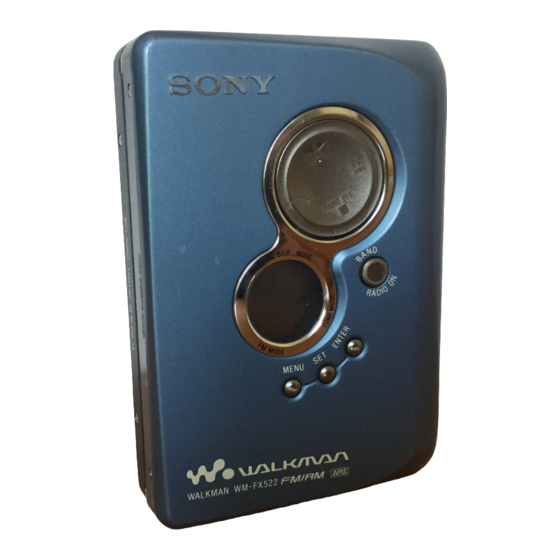
Sony WM-FX522 Service Manual
Hide thumbs
Also See for WM-FX522:
- Manual de instrucciones (2 pages) ,
- Operating instructions (2 pages) ,
- Operating instructions (2 pages)
Table of Contents
Advertisement
Quick Links
SERVICE MANUAL
Ver 1.0 2003.01
Radio section
Frequency range
FM: 87.5 - 108 MHz
AM: 531 - 1 602 kHz
Tape section
Frequency response
Playback: 40 - 15 000 Hz
Output
Headphones (i) jack
Load impedance 8 - 300 Ω
General
Power requirements
1.5 V
One R6 (size AA) battery
Dimensions (w/h/d)
Approx. 77.0 × 108.4 × 28.7 mm, excl. projecting parts and
controls
Mass
Approx. 165 g (main unit only)
Sony Corporation
9-874-226-01
2003A0500-1
Personal Audio Company
C 2003.01
Published by Sony Engineering Corporation
WM-FX522
Model Name Using Similar Mechanism
Tape Transport Mechanism Type
SPECIFICATIONS
Supplied accessories
• Stereo headphones/earphones with remote control or stereo
headphones/earphones (1)
Design and specifications are subject to change without notice.
Battery life* (Approx. hours)
Sony alkaline LR6 (SG)**
* Measured value by the standard of JEITA (Japan Electronics
and Information Technology Industries Association). (Using
a Sony HF series cassette tape)
**When using a Sony LR6 (SG) "STAMINA" alkaline dry
battery (produced in Japan).
Note
• The battery life may be shorter depending on the
operating condition, the surrounding temperature
and battery type.
RADIO CASSETTE PLAYER
AEP Model
WM-FX521
MT-WMEX505-162
Tape playback Radio reception
35
65
Advertisement
Table of Contents

Related Manuals for Sony WM-FX522


Summary of Contents for Sony WM-FX522
- Page 1 * Measured value by the standard of JEITA (Japan Electronics and Information Technology Industries Association). (Using General a Sony HF series cassette tape) Power requirements **When using a Sony LR6 (SG) “STAMINA” alkaline dry 1.5 V battery (produced in Japan). One R6 (size AA) battery Dimensions (w/h/d) Note Approx.
-
Page 2: Table Of Contents
WM-FX522 TABLE OF CONTENTS Notes on chip component replacement • Never reuse a disconnected chip component. • Notice that the minus side of a tantalum capacitor may be dam- SERVICING NOTES ..........3 aged by heat. GENERAL ..............5 Flexible Circuit Board Repairing •... -
Page 3: Servicing Notes
WM-FX522 SECTION 1 SERVICING NOTES This set detects the rotation of the idler gear (A) (side S) using the FF, REW modes PH701 (photo reflector). The PH701 is mounted on the MAIN (1) Check that the preset state is set. - Page 4 WM-FX522 SLIDER (NRA) Rotation system Rotation system during PLAY gear (NR) (FWD: left side REW: right side) idler (A) gear (T side) idler (A) gear (S side) gear (REEL) (S side) gear (REEL) (T side) slider (NRA) motor pulley cam gear...
-
Page 5: General
WM-FX522 SECTION 2 This section is extracted from instruction manual. GENERAL RADIO ON/ BAND•OFF OPEN TUNE/PRESET – TUNE/PRESET – TUNE/PRESET + TUNE/PRESET + RADIO OFF RADIO OFF BAND• BAND• RADIO ON RADIO ON ENTER PRESET + ENTER PRESET – MENU... -
Page 6: Disassembly
WM-FX522 SECTION 3 DISASSEMBLY • This set can be disassembled in the order shown below. 3-1. DISASSEMBLY FLOW Note 1: The process described in can be performed in any order. Note 2: Without completing the process described in , the next process can not be performed. -
Page 7: Case Block Assy
WM-FX522 3-3. CASE BLOCK ASSY S701 On installation case block assy, adjust the S701 and knob (hold). knob (hold) 1 three screws (M1.4) 1 two screws (M1.4) 2 Remove the case block assy to direction of the arrow. 3-4. ORNAMENT REEL... -
Page 8: Battery Holder
WM-FX522 3-5. BATTERY HOLDER 2 two screws 3 battery holder 1 Break the soldering 1 Break the soldering of battery terminal (–). of battery terminal (+). 3-6. BELT (F2) 1 belt (F2) (See page 4) -
Page 9: Main Board
WM-FX522 3-7. MAIN BOARD 2 screw (M1.4) 1 Remove four solders of motor. flexible board 1 Remove two solders of plunger solenoid. 1 Remove six solders of flexible board. 1 Remove four solders of leaf switch. 3 main board NOTE FOR INSTALLATION •... -
Page 10: Motor (Capstan/Reel) (M901)
WM-FX522 3-8. MOTOR (CAPSTAN/REEL) (M901) 1 two screws (M1.4) 2 motor (capstan/reel) (M901) 3-9. HOLDER (FS) ASSY 2 boss 7 bracket (cassette) assy (/M) 5 lock lever (S) (/M) 3 lock lever (B) (/M) 1 two screws 4 screw (M1.4) -
Page 11: Pinch Lever (N) Assy, Pinch Lever (R) Assy
WM-FX522 3-10. PINCH LEVER (N) ASSY, PINCH LEVER (R) ASSY 1 claw 2 Remove the pinch lever (R) assy to direction of the arrow. 4 Remove the pinch lever (N) assy to direction of the arrow. 3 claw 3-11. MAGNETIC HEAD (PLAYBACK) (HP901) -
Page 12: Mechanical Adjustments
WM-FX522 SECTION 4 SECTION 5 MECHANICAL ADJUSTMENTS ELECTRICAL ADJUSTMENTS PRECAUTION PRECAUTION 1. Clean the following parts with a denatured-alcohol-moistened 1. Specified voltage: 1.3 V (DC) swab: 2. Setting playback head pinch roller : OFF rubber belts capstan AVLS : OFF 2. - Page 13 WM-FX522 TUNER SECTION 0 dB=1 µV digital voltmeter [AM] Setting: TP5 (VT) – function : RADIO BAND button : AM Put the lead-wire • AM alignment should be done with mechadeck attached. AM RF signal antenna close to • Repeat the procedures in each adjustment several times for a...
- Page 14 WM-FX522 MEMO...
-
Page 15: Diagrams
WM-FX522 SECTION 6 DIAGRAMS 6-1. BLOCK DIAGRAM – TUNER Section – FM/AM IF AMP, FM/AM DET, MPX IC1 (2/2) FM RF AMP, FM/AM MIX AMP, FM/AM OSC, IC1 (1/2) FMRFIN FM-MIX B.P.F. FMIFIN L-OUT TUNER L-CH DETOUT MPXIN IF AMP... -
Page 16: Block Diagram - Main Section
WM-FX522 6-2. BLOCK DIAGRAM – MAIN Section – TUNER L-CH (Page 15) (Page 15) AUDIO MASTER AMP AUDIO MASTER AMP (FWD/REV SELECT, PLAYBACK EQ AMP) (BASS BOOST AMP, AMS, POWER AMP) HP901 J301 IC301 (1/3) RV301 IC301 (2/3) (PLAYBACK) • R-ch is omitted due to same as L-ch. -
Page 17: Note For Printed Wiring Board And Schematic Diagrams
WM-FX522 6-3. NOTE FOR PRINTED WIRING BOARD AND SCHEMATIC DIAGRAMS • Waveforms Note on Printed Wiring Board: Note on Schematic Diagram: 1 IC701 ua (XOUT) • X : parts extracted from the component side. • All capacitors are in µF unless otherwise noted. pF: µµF •... -
Page 18: Schematic Diagram - Main Board (1/2)
WM-FX522 6-4. SCHEMATIC DIAGRAM – MAIN Board (1/2) – • See page 21 for IC Block Diagrams. (1/2) CT1, L5 (VT) SVC347 2200p 100k 0.022 470p 100p 100k MA2S357 470k 470k MA2S357 1000p FERRITE-ROD FM RF ANTENNA 2200p AM OSC... -
Page 19: Schematic Diagram - Main Board (2/2)
WM-FX522 6-5. SCHEMATIC DIAGRAM – MAIN Board (2/2) – • • See page 17 for Waveforms. See page 21 for IC Block Diagrams. (2/2) LCD1 LIQUID CRYSTAL DISPLAY R706 220k R701 R703 R715 R702 S701 R707 220k 470k 220k HOLD L701 22µH... -
Page 20: Printed Wiring Board
WM-FX522 6-6. PRINTED WIRING BOARD MAIN BOARD (COMPONENT SIDE) AM FERRITE-ROD MAIN BOARD ANTENNA J301 S701 (CONDUCTOR SIDE) HOLD HP901 HOLD (PLAYBACK) RV301 R-CH S901-1 –1 (TAPE DETECT) L-CH –2 TP61 (FM RF IN) R-CH S901-2 (GND) B. P. F. -
Page 21: Ic Block Diagrams
WM-FX522 • IC Block Diagrams IC1 TA2154FN-(EL) BUFFER FM/AM/TV PW SW 1/8 OR 1/16 LEVEL BUFFER BUFFER FM MPX FM/TV BUFFER IC301 TA2123AF (EL) 36 35 – RF IN PW GND – OUT B PW B OUT C C-AMP SW 37... - Page 22 WM-FX522 IC601 MM1279XVBE PRE DRIVER MOTIVE CONTROL CIRCUIT MOTIVE/ MOTIVE SOFT SWITCH LOGIC BIAS VREF SPEED CURRENT REFERENCE CONTROL CONTROL START VOLTAGE OUTPUT INVERTER BIAS – IN+ 10 IC801 XC6383C251ML CHIP ENABLE VLx LIMITER V OUT V REF 2 STEP PFM CONTROL BUFFER –...
-
Page 23: Ic Pin Function Description
WM-FX522 6-7. IC PIN FUNCTION DESCRIPTION • IC701 TC9328AF-108 (SYSTEM CONTROLLER, LIQUID CRYSTAL DISPLAY DRIVER) Pin No. Pin Name Description 1 to 4 COM1 to COM4 Common drive signal output to the liquid crystal display 5 to 21 SEG1 to SEG17... - Page 24 WM-FX522 Pin No. Pin Name Description Power on/off control signal output of the tuner circuit RADIO ON “L”: power on (tuner on), “H”: power off (tape on) Not used System reset signal input “L”: reset RESET For several hundreds msec. after the power supply rises, “L” is input, then it changes to “H”...
-
Page 25: Exploded Views
WM-FX522 SECTION 7 EXPLODED VIEWS NOTE: • -XX and -X mean standardized parts, so they • Items marked “*” are not stocked since they may have some difference from the original are seldom required for routine service. Some one. delay should be anticipated when ordering •... -
Page 26: Bracket, Main Board Section
WM-FX522 7-2. BRACKET, MAIN BOARD SECTION supplied S901 MT-WMEX505-162 main board LCD1 not supplied Ref. No. Part No. Description Remark Ref. No. Part No. Description Remark 3-375-114-81 SCREW 3-939-590-05 SCREW (IB LOCK) 3-042-004-01 TERMINAL (+), BATTERY 3-038-054-01 LEVER (B) (/M), LOCK... -
Page 27: Mechanism Deck Section (Mt-Wmex505-162)
WM-FX522 7-3. MECHANISM DECK SECTION (MT-WMEX505-162) M901 PM901 HP901 Ref. No. Part No. Description Remark Ref. No. Part No. Description Remark X-3378-354-5 HOLDER (FS) ASSY 3-007-433-01 SHEET (N), REFLECTION X-3377-363-1 LEVER (R) ASSY, PINCH X-3378-107-3 CHASSIS ASSY (FB) 3-046-789-01 SPRING (HDA) -
Page 28: Electrical Parts List
WM-FX522 SECTION 8 ELECTRICAL PARTS LIST MAIN NOTE: When indicating parts by reference • Due to standardization, replacements in the • Items marked “*” are not stocked since they number, please include the board. parts list may be different from the parts speci- are seldom required for routine service. - Page 29 WM-FX522 MAIN Ref. No. Part No. Description Remark Ref. No. Part No. Description Remark C410 1-107-819-11 CERAMIC CHIP 0.022uF 1-414-760-21 FERRITE C411 1-164-937-11 CERAMIC CHIP 0.001uF C412 1-165-128-11 CERAMIC CHIP 0.22uF < BAND PASS FILTER > C414 1-164-935-11 CERAMIC CHIP...
- Page 30 WM-FX522 MAIN Ref. No. Part No. Description Remark Ref. No. Part No. Description Remark 1-218-957-11 RES-CHIP 2.2K 1/16W 1-218-957-11 RES-CHIP 2.2K 1/16W R501 1-218-953-11 RES-CHIP 1/16W 1-218-957-11 RES-CHIP 2.2K 1/16W R601 1-218-969-11 RES-CHIP 1/16W 1-216-845-11 METAL CHIP 100K 1/10W R602...
- Page 31 WM-FX522 MAIN Ref. No. Part No. Description Remark Ref. No. Part No. Description Remark < TRANSFORMER > T401 1-437-599-21 TRANSFORMER, DC/DC CONVERTER < THERMISTOR > TH601 1-810-794-11 THERMISTOR, POSITIVE < CERAMIC FILTER/VIBRATOR > 1-795-410-21 FILTER, CERAMIC X701 1-577-262-11 VIBRATOR, CRYSTAL (75kHz)
-
Page 32: Revision History
WM-FX522 REVISION HISTORY Clicking the version allows you to jump to the revised page. Also, clicking the version at the upper right on the revised page allows you to jump to the next revised page. Ver. Date Description of Revision...